

MICRON MT4LC4M16R6TG-6IT, MT4LC4M16R6TG-6S, MT4LC4M16R6TG-5, MT4LC4M16R6TG-5IT, MT4LC4M16R6TG-5S Datasheet
...
1
4 Meg x 16 EDO DRAM Micron Technology, Inc., reserves the right to change products or specifications without notice.
D29_2.p65 – Rev. 5/00 ©2000, Micron Technology, Inc.
4 MEG x 16
EDO DRAM
FEATURES
• Single +3.3V ±0.3V power supply
• Industry-standard x16 pinout, timing, functions,
and package
• 12 row, 10 column addresses (R6)
13 row, 9 column addresses (N3)
• High-performance CMOS silicon-gate process
• All inputs, outputs and clocks are LVTTL-compatible
• Extended Data-Out (EDO) PAGE MODE access
• 4,096-cycle CAS#-BEFORE-RAS# (CBR) REFRESH
distributed across 64ms
• Optional self refresh (S) for low-power data
retention
OPTIONS MARKING
• Plastic Package
50-pin TSOP (400 mil) TG
• Timing
50ns access -5
60ns access -6
• Refresh Rates
4K R6
8K N3
Standard Refresh None
Self Refresh S*
• Operating Temperature Range
Commercial (0°C to +70°C) None
Extended (-40°C to +85°C) IT**
NOTE: 1. The “#” symbol indicates signal is active LOW.
*Contact factory for availability.
**Available only on MT4LC4M16R6 standard refresh device.
Part Number Example:
MT4LC4M16R6TG-5
PIN ASSIGNMENT (Top View)
DRAM
MT4LC4M16R6, MT4LC4M16N3
For the latest data sheet, please refer to the Micron Web
site: www.micronsemi.com/mti/msp/html/datasheet.html
VCC
DQ0
DQ1
DQ2
DQ3
V
CC
DQ4
DQ5
DQ6
DQ7
NC
V
CC
WE#
RAS#
NC
NC
NC
NC
A0
A1
A2
A3
A4
A5
V
CC
1
2
3
4
5
6
7
8
9
10
11
12
13
14
15
16
17
18
19
20
21
22
23
24
25
50
49
48
47
46
45
44
43
42
41
40
39
38
37
36
35
34
33
32
31
30
29
28
27
26
V
SS
DQ15
DQ14
DQ13
DQ12
V
SS
DQ11
DQ10
DQ9
DQ8
NC
V
SS
CASL#
CASH#
OE#
NC
NC
NC/A12
†
A11
A10
A9
A8
A7
A6
V
SS
KEY TIMING PARAMETERS
SPEEDtRCtRACtPC
t
AAtCACtCAS
-5 84ns 50ns 20ns 25ns 13ns 8ns
-6 104ns 60ns 25ns 30ns 15ns 10ns
50-Pin TSOP
4 MEG x 16 EDO DRAM PART NUMBERS
REFRESH
PART NUMBER ADDRESSING PACKAGE REFRESH
MT4LC4M16R6TG-x 4K 400-TSOP Standard
MT4LC4M16R6TG-x S 4K 400-TSOP Self
MT4LC4M16N3TG-x 8K 400-TSOP Standard
MT4LC4M16N3TG-x S 8K 400-TSOP Self
x = speed
MT4LC4M16R6 MT4LC4M16N3
Configuration 4 Meg x 16 4 Meg x 16
Refresh 4K 8K
Row Address 4K (A0-A11) 8K (A0-A12)
Column Addressing 1K (A0-A9) 512 (A0-A8)
†
A12 for N3 version, NC for R6 version.
2
4 Meg x 16 EDO DRAM Micron Technology, Inc., reserves the right to change products or specifications without notice.
D29_2.p65 – Rev. 5/00 ©2000, Micron Technology, Inc.
4 MEG x 16
EDO DRAM
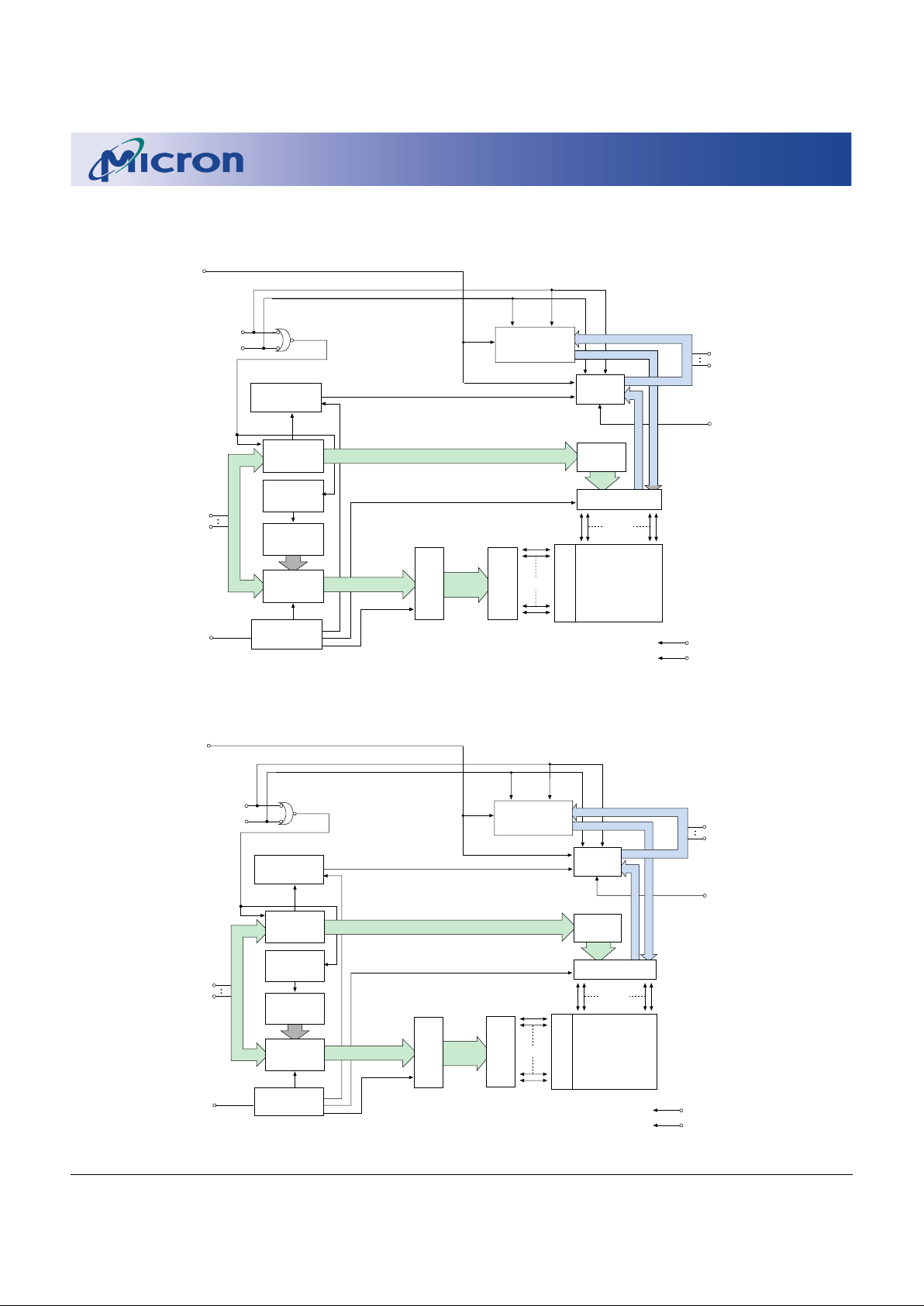
A0-
A11
RAS#
12
12
10
REFRESH
CONTROLLER
NO. 1 CLOCK
GENERATOR
V
DD
V
SS
12
10
COLUMN-
ADDRESS
BUFFER(10)
ROW-
ADDRESS
BUFFERS (12)
4,096
1,024
COLUMN
DECODER
16
REFRESH
COUNTER
ROW SELECT
ROW
DECODER
4,096 x 1,024 x 16
MEMORY
ARRAY
COMPLEMENT
SELECT
1,024 x 16
4,096 x 16
NO. 2 CLOCK
GENERATOR
WE#
OE#
DQ0DQ15
16
16
DATA-OUT
BUFFER
CASL#
CAS#
CASH#
DATA-IN BUFFER
16
SENSE AMPLIFIERS
I/O GATING
FUNCTIONAL BLOCK DIAGRAM
MT4LC4M16R6 (12 row addresses)
A0-
A12
RAS#
13
13
9
NO. 2 CLOCK
GENERATOR
REFRESH
CONTROLLER
NO. 1 CLOCK
GENERATOR
Vcc
Vss
13
WE#
9
COLUMN-
ADDRESS
BUFFER(9)
ROW-
ADDRESS
BUFFERS (13)
8192
512
COLUMN
DECODER
OE#
DQ0DQ15
16
16
16
16
REFRESH
COUNTER
ROW SELECT
ROW
DECODER
SENSE AMPLIFIERS
I/O GATING
DATA-OUT
BUFFER
8192 x 512 x 16
MEMORY
ARRAY
COMPLEMENT
SELECT
512 x 16
8192 x 16
CASL#
CAS#
CASH#
DATA-IN BUFFER
FUNCTIONAL BLOCK DIAGRAM
MT4LC4M16N3 (13 row addresses)

3
4 Meg x 16 EDO DRAM Micron Technology, Inc., reserves the right to change products or specifications without notice.
D29_2.p65 – Rev. 5/00 ©2000, Micron Technology, Inc.
4 MEG x 16
EDO DRAM
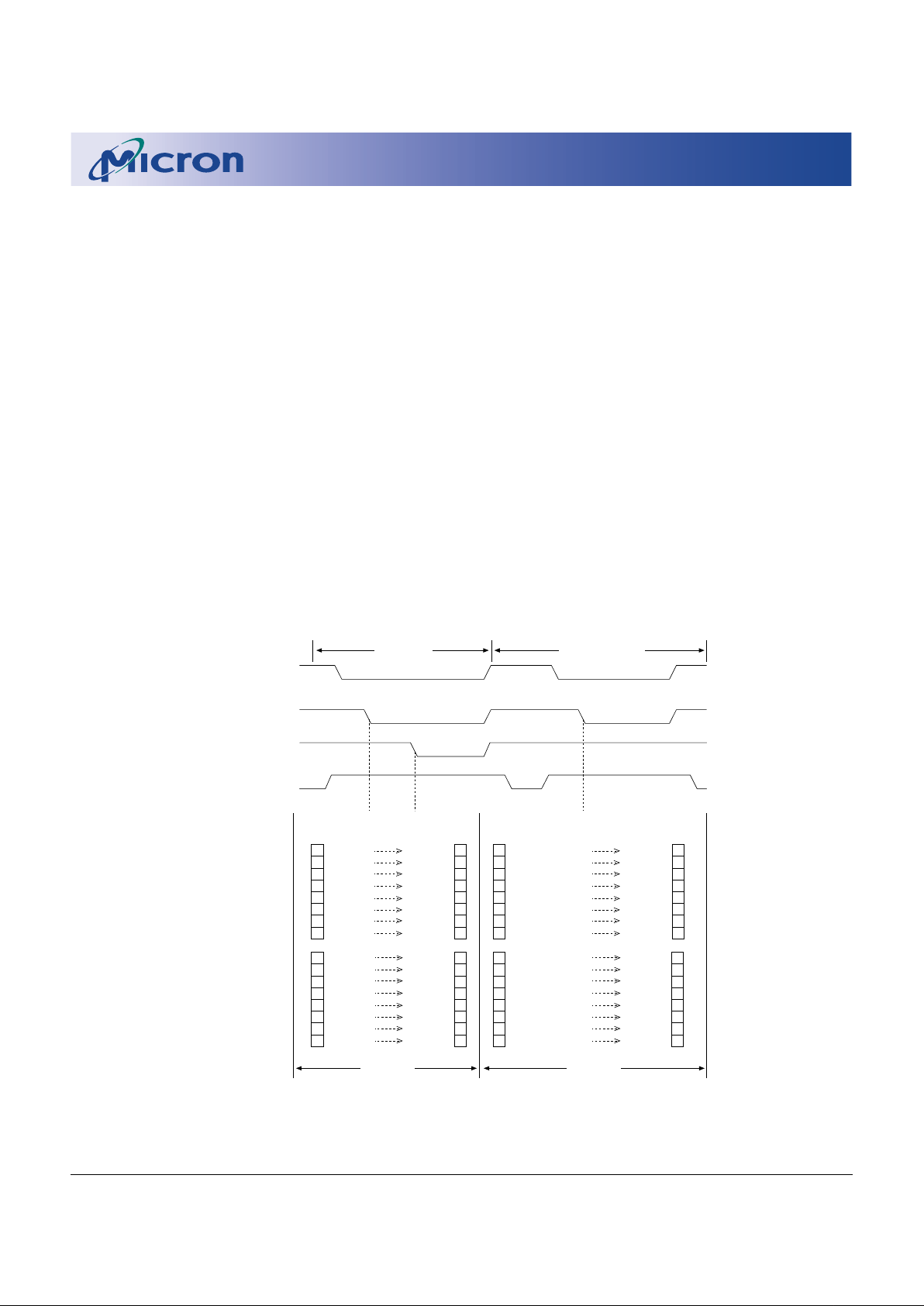
Figure 1
WORD and BYTE WRITE Example
STORED
DATA
1
1
0
1
1
1
1
1
RAS#
CASL#
WE#
X = NOT EFFECTIVE (DON'T CARE)
ADDRESS 1ADDRESS 0
0
1
0
1
0
0
0
0
WORD WRITE LOWER BYTE WRITE
CASH#
INPUT
DATA
0
0
1
0
0
0
0
0
1
0
1
0
1
1
1
1
X
X
X
X
X
X
X
X
INPUT
DATA
1
1
0
1
1
1
1
1
INPUT
DATA
STORED
DATA
1
1
0
1
1
1
1
1
INPUT
DATA
STORED
DATA
0
0
1
0
0
0
0
0
1
0
1
0
1
1
1
1
STORED
DATA
0
0
1
0
0
0
0
0
1
0
1
0
1
1
1
1
X
X
X
X
X
X
X
X
1
0
1
0
1
1
1
1
UPPER BYTE
(DQ8-DQ15)
OF WORD
LOWER BYTE
(DQ0-DQ7)
OF WORD
GENERAL DESCRIPTION
The 4 Meg x 16 DRAM is a high-speed CMOS,
dynamic random-access memory device containing
67,108,864 bits and designed to operate from 3V to
3.6V. The device is functionally organized as 4,194,304
locations containing 16 bits each. The 4,194,304
memory locations are arranged in 4,096 rows by 1,024
columns on the MT4LC4M16R6 or 8,192 rows by 512
columns on the MT4LC4M16N3. During READ or WRITE
cycles, each location is uniquely addressed via the
address bits: 12 row-address bits (A0-A11) and 10
column-address bits (A0-A9) on the MT4LC4M16R6 or
13 row-address bits (A0-A12) and 9 column-address bits
(A0-A8) on the MT4LC4M16N3 version. In addition,
both byte and word accesses are supported via the two
CAS# pins (CASL# and CASH#).
The CAS# functionality and timing related to address and control functions (e.g., latching column
addresses or selecting CBR REFRESH) is such that the
internal CAS# signal is determined by the first external
CAS# signal (CASL# or CASH#) to transition LOW and
the last to transition back HIGH. The CAS# functionality and timing related to driving or latching data is such
that each CAS# signal independently controls the associated eight DQ pins.
The row address is latched by the RAS# signal, then
the column address is latched by CAS#. This device
provides EDO-PAGE-MODE operation, allowing for fast
successive data operations (READ, WRITE or READMODIFY-WRITE) within a given row.
The 4 Meg x 16 DRAM must be refreshed periodically in order to retain stored data.
DRAM ACCESS
Each location in the DRAM is uniquely addressable,
as mentioned in the General Description. Use of both
CAS# signals results in a word access via the 16 I/O pins
(DQ0-DQ15). Using only one of the two signals results
in a BYTE access cycle. CASL# transitioning LOW selects an access cycle for the lower byte (DQ0-DQ7), and
CASH# transitioning LOW selects an access cycle for
4
4 Meg x 16 EDO DRAM Micron Technology, Inc., reserves the right to change products or specifications without notice.
D29_2.p65 – Rev. 5/00 ©2000, Micron Technology, Inc.
4 MEG x 16
EDO DRAM
the upper byte (DQ8-DQ15). General byte and word
access timing is shown in Figures 1 and 2.
A logic HIGH on WE# dictates read mode, while a
logic LOW on WE# dictates write mode. During a
WRITE cycle, data-in (D) is latched by the falling edge
of WE or CAS# (CASL# or CASH#), whichever occurs
last. An EARLY WRITE occurs when WE is taken LOW
prior to either CAS# falling. A LATE WRITE or READMODIFY-WRITE occurs when WE falls after CAS# (CASL#
or CASH#) is taken LOW. During EARLY WRITE cycles,
the data outputs (Q) will remain High-Z, regardless of
the state of OE#. During LATE WRITE or READ-MODIFYWRITE cycles, OE# must be taken HIGH to disable the
data outputs prior to applying input data. If a LATE
WRITE or READ-MODIFY-WRITE is attempted while
keeping OE# LOW, no write will occur, and the data
outputs will drive read data from the accessed location.
Additionally, both bytes must always be of the same
mode of operation if both bytes are active. A CAS#
precharge must be satisfied prior to changing modes of
operation between the upper and lower bytes. For
example, an EARLY WRITE on one byte and a LATE
Figure 2
WORD and BYTE READ Example
STORED
DATA
1
1
0
1
1
1
1
1
RAS#
CASL#
WE#
Z = High-Z
ADDRESS 1ADDRESS 0
0
1
0
1
0
0
0
0
WORD READ LOWER BYTE READ
STORED
DATA
1
1
0
1
1
1
1
1
CASH#
OUTPUT
DATA
1
1
0
1
1
1
1
1
STORED
DATA
1
1
0
1
1
1
1
1
Z
Z
Z
Z
Z
Z
Z
Z
OUTPUT
DATA
1
1
0
1
1
1
1
1
OUTPUT
DATA
1
1
0
1
1
1
1
1
OUTPUT
DATA
1
1
0
1
1
1
1
1
STORED
DATA
1
1
0
1
1
1
1
1
UPPER BYTE
(DQ8-DQ15)
OF WORD
LOWER BYTE
(DQ0-DQ7)
OF WORD
0
1
0
1
0
0
0
0
0
1
0
1
0
0
0
0
Z
Z
Z
Z
Z
Z
Z
Z
Z
Z
Z
Z
Z
Z
Z
Z
0
1
0
1
0
0
0
0
0
1
0
1
0
0
0
0
WRITE on the other byte are not allowed during the
same cycle. However, an EARLY WRITE on one byte and
a LATE WRITE on the other byte, after a CAS# precharge
has been satisfied, are permissible.
EDO PAGE MODE
DRAM READ cycles have traditionally turned the
output buffers off (High-Z) with the rising edge of
CAS#. If CAS# went HIGH and OE# was LOW (active),
the output buffers would be disabled. The 64Mb EDO
DRAM offers an accelerated page mode cycle by eliminating output disable from CAS# HIGH. This option is
called EDO, and it allows CAS# precharge time (tCP) to
occur without the output data going invalid (see READ
and EDO-PAGE-MODE READ waveforms).
EDO operates like any DRAM READ or FAST-PAGEMODE READ, except data is held valid after CAS# goes
HIGH, as long as RAS# and OE# are held LOW and WE#
is held HIGH. OE# can be brought LOW or HIGH while
CAS# and RAS# are LOW, and the DQs will transition
between valid data and High-Z. Using OE#, there are
DRAM ACCESS (continued)
5
4 Meg x 16 EDO DRAM Micron Technology, Inc., reserves the right to change products or specifications without notice.
D29_2.p65 – Rev. 5/00 ©2000, Micron Technology, Inc.
4 MEG x 16
EDO DRAM
Figure 3
OE# Control of DQs
V
V
IH
IL
CAS#
V
V
IH
IL
RAS#
V
V
IH
IL
ADDR
ROW COLUMN (A)
COLUMN (B)
V
V
IH
IL
OE#
V
V
IOH
IOL
OPEN
DQ
t
OD
VALID DATA (B)
VALID DATA (A)
COLUMN (C)
VALID DATA (A)
t
OE
VALID DATA (C)
COLUMN (D)
VALID DATA (D)
t
OD
t
OEHC
t
OD
t
OEP
t
OES
The DQs go back to
Low-Z if
t
OES is met.
The DQs remain High-Z
until the next CAS# cycle
if
t
OEHC is met.
The DQs remain High-Z
until the next CAS# cycle
if
t
OEP is met.
Figure 4
WE# Control of DQs
V
V
IH
IL
CAS#
V
V
IH
IL
RAS#
V
V
IH
IL
ADDR
ROW COLUMN (A)
DON’T CARE
UNDEFINED
V
V
IH
IL
WE#
V
V
IOH
IOL
OPEN
DQ
t
WPZ
The DQs go to High-Z if WE# falls and, if tWPZ is met,
will remain High-Z until CAS# goes LOW with
WE# HIGH (i.e., until a READ cycle is initiated).
V
V
IH
IL
OE#
VALID DATA (B)
t
WHZ
WE# may be used to disable the DQs to prepare
for input data in an EARLY WRITE cycle. The DQs
will remain High-Z until CAS# goes LOW with
WE# HIGH (i.e., until a READ cycle is initiated).
t
WHZ
COLUMN (D)
VALID DATA (A)
COLUMN (B)
COLUMN (C)
INPUT DATA (C)

6
4 Meg x 16 EDO DRAM Micron Technology, Inc., reserves the right to change products or specifications without notice.
D29_2.p65 – Rev. 5/00 ©2000, Micron Technology, Inc.
4 MEG x 16
EDO DRAM
two methods to disable the outputs and keep them
disabled during the CAS# HIGH time. The first method
is to have OE# HIGH when CAS# transitions HIGH and
keep OE# HIGH for tOEHC thereafter. This will disable
the DQs, and they will remain disabled (regardless of
the state of OE# after that point) until CAS# falls again.
The second method is to have OE# LOW when CAS#
transitions HIGH and then bring OE# HIGH for a
minimum of tOEP anytime during the CAS# HIGH
period. This will disable the DQs, and they will remain
disabled (regardless of the state of OE# after that point)
until CAS# falls again (see Figure 3). During other
cycles, the outputs are disabled at tOFF time after RAS#
and CAS# are HIGH or at tWHZ after WE# transitions
LOW. The tOFF time is referenced from the rising edge
of RAS# or CAS#, whichever occurs last. WE# can also
perform the function of disabling the output drivers
under certain conditions, as shown in Figure 4.
EDO-PAGE-MODE operations are always initiated
with a row address strobed in by the RAS# signal,
followed by a column address strobed in by CAS#, just
like for single location accesses. However, subsequent
column locations within the row may then be accessed
at the page mode cycle time. This is accomplished by
cycling CAS# while holding RAS# LOW and entering
new column addresses with each CAS# cycle. Returning
RAS# HIGH terminates the EDO-PAGE-MODE
operation.
DRAM REFRESH
The supply voltage must be maintained at the specified levels, and the refresh requirements must be met in
order to retain stored data in the DRAM. The refresh
requirements are met by refreshing all rows in the
4 Meg x 16 DRAM array at least once every 64ms (8,192
rows for N3 or 4,096 rows for R6). The recommended
procedure is to execute 4,096 CBR REFRESH cycles,
either uniformly spaced or grouped in bursts, every
64ms. The MT4LC4M16N3 internally refreshes two
rows for each CBR cycle, whereas the MT4LC4M16R6
refreshes one row for every CBR cycle. For either device,
executing 4,096 CBR cycles will refresh the entire device. The CBR REFRESH will invoke the internal refresh
counter for automatic RAS# addressing. Alternatively,
RAS#-ONLY REFRESH capability is inherently provided.
However, with this method, only one row is refreshed
on each cycle. Thus, 8,192 RAS-only REFRESH cycles are
needed every 64ms on the MT4LC4M16N3 in order to
refresh the entire device. JEDEC strongly recommends
the use of CBR REFRESH for this device.
An optional self refresh mode is also available on the
“S” version. The self refresh feature is initiated by
performing a CBR Refresh cycle and holding RAS# low
for the specified tRASS. The “S” option allows the user
the choice of a fully static, low-power data retention
mode or a dynamic refresh mode at the extended
refresh period of 128ms, or 31.25µs per cycle, when
using a distributed CBR refresh. This refresh rate can be
applied during normal operation, as well as during a
standby or battery backup mode.
The self refresh mode is terminated by driving RAS#
HIGH for a minimum time of tRPS. This delay allows for
the completion of any internal refresh cycles that may
be in process at the time of the RAS# LOW-to-HIGH
transition. If the DRAM controller uses a distributed
CBR refresh sequence, a burst refresh is not required
upon exiting self refresh, however, if the controller is
using RAS# only or burst CBR refresh then a burst
refresh using tRC (MIN) is required.
EDO PAGE MODE (continued)
7
4 Meg x 16 EDO DRAM Micron Technology, Inc., reserves the right to change products or specifications without notice.
D29_2.p65 – Rev. 5/00 ©2000, Micron Technology, Inc.
4 MEG x 16
EDO DRAM
ABSOLUTE MAXIMUM RATINGS*
Voltage on VCC Relative to VSS................-1V to +4.6V
Voltage on NC, Inputs or I/O Pins
Relative to VSS ....................................... -1V to +4.6V
Operating Temperature, TA (ambient)
Commercial ......................................... 0°C to +70°C
Extended (IT) ................................. -40°C to +85°C**
Storage Temperature (plastic) ............ -55°C to +150°C
Power Dissipation ................................................... 1W
*Stresses greater than those listed under “Absolute
Maximum Ratings” may cause permanent damage to
the device. This is a stress rating only, and functional
operation of the device at these or any other conditions
above those indicated in the operational sections of
this specification is not implied. Exposure to absolute
maximum rating conditions for extended periods may
affect reliability.
**Available only on MT4LC4M16R6 standard refresh
device.
DC ELECTRICAL CHARACTERISTICS AND OPERATING CONDITIONS
(Note: 1) (VCC = +3.3V ±0.3V)
PARAMETER/CONDITION SYMBOL MIN MAX UNITS NOTES
SUPPLY VOLTAGE VCC 3 3.6 V
INPUT HIGH VOLTAGE:
Valid Logic 1; All inputs, I/Os and any NC VIH 2VCC + 0.3 V 35
INPUT LOW VOLTAGE:
Valid Logic 0; All inputs, I/Os and any NC VIL -0.3 0.8 V 35
INPUT LEAKAGE CURRENT:
Any input at VIN (0V £ VIN £ VCC + 0.3V); II -2 2 µA 36
All other pins not under test = 0V
OUTPUT HIGH VOLTAGE:
IOUT = -2mA VOH 2.4–V
OUTPUT LOW VOLTAGE:
IOUT = 2mA VOL – 0.4 V
OUTPUT LEAKAGE CURRENT:
Any output at VOUT (0V £ VOUT £ VCC + 0.3V); IOZ -5 5 µA
DQ is disabled and in High-Z state
8
4 Meg x 16 EDO DRAM Micron Technology, Inc., reserves the right to change products or specifications without notice.
D29_2.p65 – Rev. 5/00 ©2000, Micron Technology, Inc.
4 MEG x 16
EDO DRAM
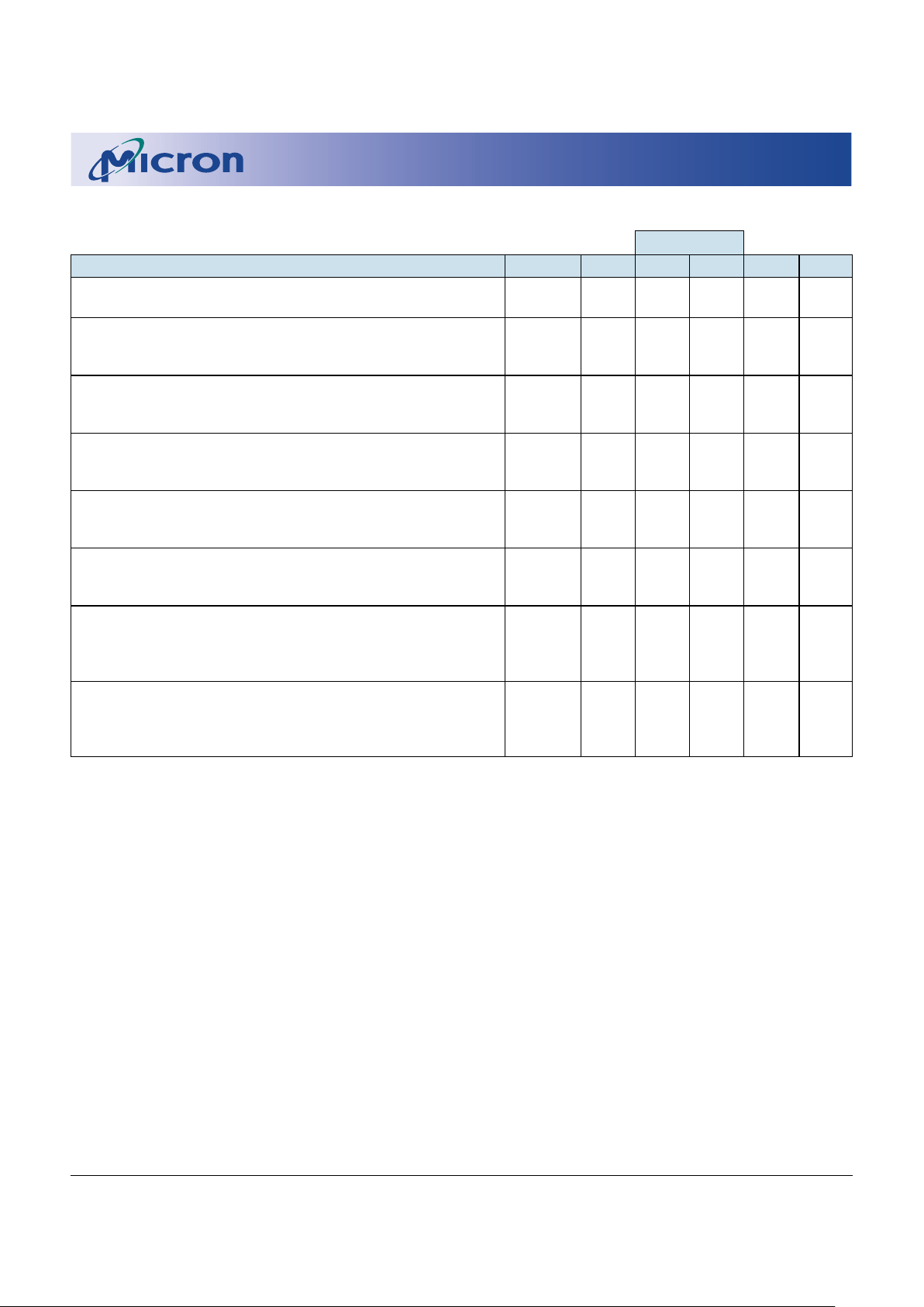
Icc OPERATING CONDITIONS AND MAXIMUM LIMITS
(Notes: 1, 2, 3, 5, 6) (VCC = +3.3V ±0.3V)
PARAMETER/CONDITION SYMBOL SPEED 4K 8K UNITS NOTES
STANDBY CURRENT: TTL ICC1 ALL 1 1 mA
(RAS# = CAS# = VIH)
STANDBY CURRENT: CMOS
(RAS# = CAS# ³ VCC - 0.2V; DQs may be left open; ICC2 ALL 500 500 µA
Other inputs: VIN ³ VCC - 0.2V or VIN £ 0.2V)
OPERATING CURRENT: Random READ/WRITE ICC3 -5 150 115 mA 26
Average power supply current -6 165 130
(RAS#, CAS#, address cycling: tRC = tRC [MIN])
OPERATING CURRENT: EDO PAGE MODE ICC4 -5 120 120 mA 26
Average power supply current -6 125 125
(RAS# = VIL, CAS#, address cycling: tPC = tPC [MIN])
REFRESH CURRENT: RAS#-ONLY ICC5 -5 150 115 mA 22
Average power supply current -6 165 130
(RAS# cycling, CAS# = VIH: tRC = tRC [MIN])
REFRESH CURRENT: CBR ICC6 -5 150 150 mA 4, 7,
Average power supply current -6 165 165 23
(RAS#, CAS#, address cycling: tRC = tRC [MIN])
REFRESH CURRENT: Extended (“S” version only) ICC7 ALL 400 400 µA 4, 7,
Average power supply current: CAS# = 0.2V or CBR cycling; 23, 37
RAS# = tRAS (MIN); WE# = VCC - 0.2V; A0-A10, OE# and
DIN = VCC - 0.2V or 0.2V (DIN may be left open); tRC = 125µs
REFRESH CURRENT: Self (“S” version only) ICC8 ALL 350 350 µA 4, 7,
Average power supply current: CBR with RAS# ³ tRASS (MIN) 37
and CAS# held LOW; WE# = VCC - 0.2V; A0-A10, OE# and
DIN = VCC - 0.2V or 0.2V (DIN may be left open)
MAX
 Loading...