

MICRON MT4LC4M16F5-5, MT4LC4M16F5-6 Datasheet
1
4 Meg x 16 FPM DRAM Micron Technology, Inc., reserves the right to change products or specifications without notice.
D28_2.p65 – Rev. 5/00 ©2000, Micron Technology, Inc.
4 MEG x 16
FPM DRAM
FEATURES
• Single +3.3V ±0.3V power supply
• Industry-standard x16 pinout, timing, functions,
and packages
• 12 row, 10 column addresses
• High-performance CMOS silicon-gate process
• All inputs, outputs and clocks are LVTTL-compatible
• FAST PAGE MODE (FPM) access
• 4,096-cycle CAS#-BEFORE-RAS# (CBR) REFRESH
distributed across 64ms
OPTIONS MARKING
• Plastic Package
50-pin TSOP (400 mil) TG
• Timing
50ns access -5
60ns access -6
• Refresh Rate
Standard Refresh None
Part Number Example
MT4LC4M16F5TG-5
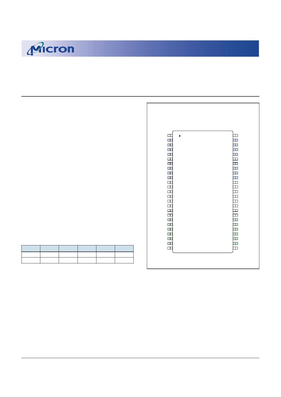
PIN ASSIGNMENT (Top View)
DRAM
MT4LC4M16F5
For the latest data sheet, please refer to the Micron
Web site: www.micron.com/mti/msp/html/
datasheet.html
50-Pin TSOP
KEY TIMING PARAMETERS
SPEED
t
RC
t
RAC
t
PC
t
AA
t
CAC
-5 90ns 50ns 30ns 25ns 13ns
-6 110ns 60ns 35ns 30ns 15ns
V
CC
DQ0
DQ1
DQ2
DQ3
V
CC
DQ4
DQ5
DQ6
DQ7
NC
V
CC
WE#
RAS#
NC
NC
NC
NC
A0
A1
A2
A3
A4
A5
V
CC
1
2
3
4
5
6
7
8
9
10
11
12
13
14
15
16
17
18
19
20
21
22
23
24
25
50
49
48
47
46
45
44
43
42
41
40
39
38
37
36
35
34
33
32
31
30
29
28
27
26
V
SS
DQ15
DQ14
DQ13
DQ12
V
SS
DQ11
DQ10
DQ9
DQ8
NC
V
SS
CASL#
CASH#
OE#
NC
NC
NC
A11
A10
A9
A8
A7
A6
V
SS
GENERAL DESCRIPTION
The 4 Meg x 16 DRAM is a high-speed CMOS,
dynamic random-access memory device containing
67,108,864 bits organized in a x16 configuration. The
MT4LC4M16F5 is functionally organized as 4,194,304
locations containing 16 bits each. The 4,194,304
memory locations are arranged in 4,096 rows by 1,024
columns. During READ or WRITE cycles, each location
is uniquely addressed via the address bits: 12 rowaddress bits (A0-A11) and 10 column-address bits (A0A9). In addition, both byte and word accesses are
supported via the two CAS# pins (CASL# and CASH#).
The CAS# functionality and timing related to address
and control functions (e.g., latching column addresses
or selecting CBR REFRESH) are such that the internal
CAS# signal is determined by the first external CAS#
signal (CASL# or CASH#) to transition LOW and the last
to transition back HIGH. The CAS# functionality and
timing related to driving or latching data are such that
each CAS# signal independently controls the associated eight DQ pins.
The row address is latched by the RAS# signal, then
the column address by CAS#. The device provides FASTPAGE-MODE operation, allowing for fast successive
data operations (READ, WRITE, or READ-MODIFYWRITE) within a given row.
The MT4LC4M16F5 must be refreshed periodi-
cally in order to retain stored data.
NOTE: 1. The # symbol indicates signal is active LOW.
2
4 Meg x 16 FPM DRAM Micron Technology, Inc., reserves the right to change products or specifications without notice.
D28_2.p65 – Rev. 5/00 ©2000, Micron Technology, Inc.
4 MEG x 16
FPM DRAM
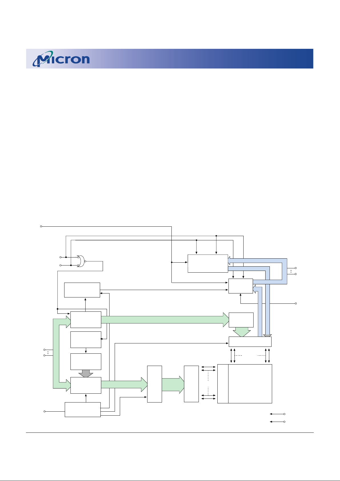
FUNCTIONAL BLOCK DIAGRAM
MT4LC4M16F5 (12 row addresses)
A0-
A11
RAS#
12
12
10
REFRESH
CONTROLLER
NO. 1 CLOCK
GENERATOR
V
DD
V
SS
12
10
COLUMNADDRESS
BUFFER(10)
ROW-
ADDRESS
BUFFERS (12)
4,096
1,024
COLUMN
DECODER
16
REFRESH
COUNTER
ROW SELECT
ROW
DECODER
4,096 x 1,024 x 16
MEMORY
ARRAY
COMPLEMENT
SELECT
1,024 x 16
4,096 x 16
NO. 2 CLOCK
GENERATOR
WE#
OE#
DQ0DQ15
16
16
DATA-OUT
BUFFER
CASL#
CAS#
CASH#
DATA-IN BUFFER
16
SENSE AMPLIFIERS
I/O GATING
FAST PAGE MODE ACCESS
Each location in the DRAM is uniquely addressable,
as mentioned in the General Description. Use of both
CAS# signals results in a word access via the 16 I/O pins
(DQ0-DQ15). Use of only one of the two results in a
BYTE access cycle. CASL# transitioning LOW selects an
access cycle for the lower byte (DQ0-DQ7), and CASH#
transitioning LOW selects an access cycle for the upper
byte (DQ8-DQ15). General byte and word access timing
is shown in Figures 1 and 2.
Additionally, both bytes must always be of the same
mode of operation if both bytes are active. A CAS#
precharge must be satisfied prior to changing modes of
operation between the upper and lower bytes. For
example, an EARLY WRITE on one byte and a LATE
WRITE on the other byte are not allowed during the
same cycle. However, an EARLY WRITE on one byte and
a LATE WRITE on the other byte, after a CAS# precharge
has been satisfied, are permissible.
The WE# signal must be activated to execute a
WRITE operation; otherwise a READ operation will be
performed. The OE# signal must be activated to enable
the DQ output drivers for a read access and can be
deactivated to disable output data if necessary.
FAST-PAGE-MODE operations are always initiated
with a row address strobed in by the RAS# signal,
followed by a column address strobed in by CAS#, just
like for single location accesses. However, subsequent
column locations within the row may then be accessed
at the page mode cycle time. This is accomplished by
cycling CAS# while holding RAS# LOW and entering
new column addresses with each CAS# cycle. Returning
RAS# HIGH terminates the FAST-PAGE-MODE
operation.
3
4 Meg x 16 FPM DRAM Micron Technology, Inc., reserves the right to change products or specifications without notice.
D28_2.p65 – Rev. 5/00 ©2000, Micron Technology, Inc.
4 MEG x 16
FPM DRAM
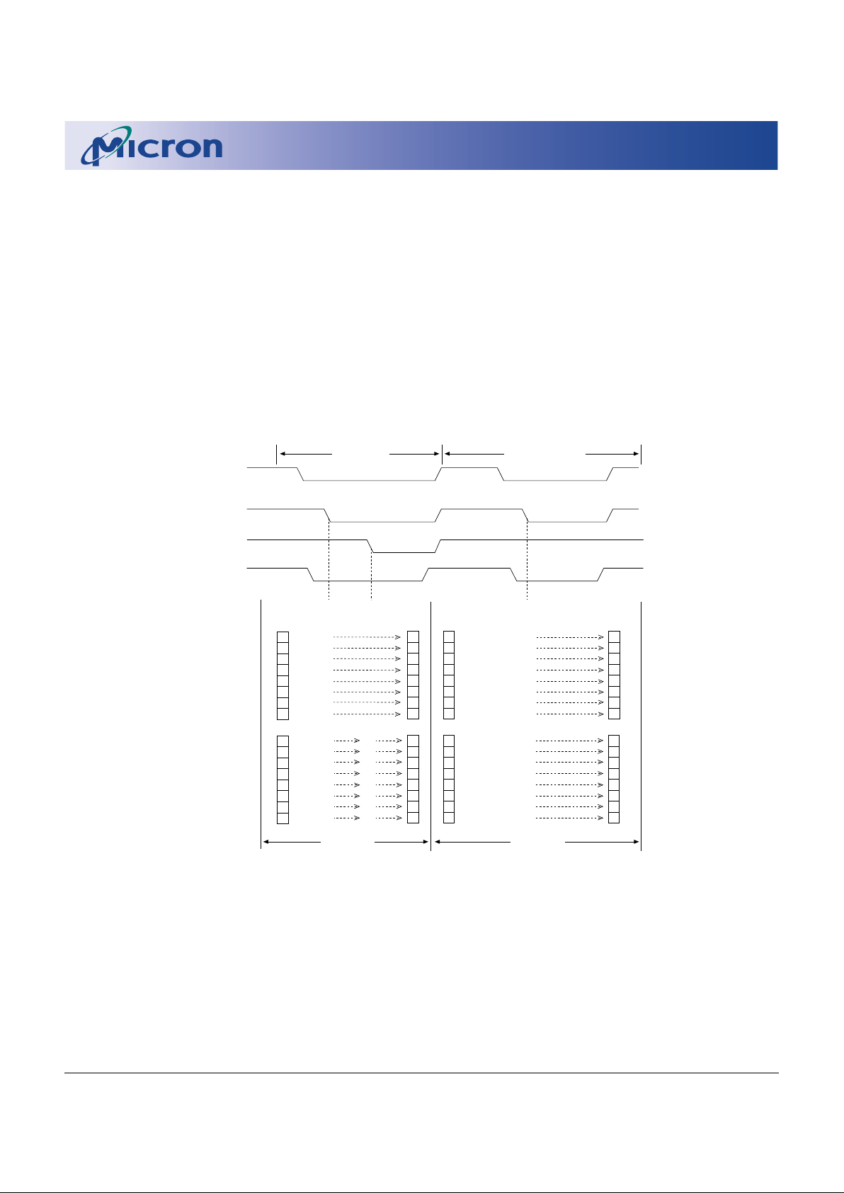
STORED
DATA
1
1
0
1
1
1
1
1
RAS#
CASL#
WE#
X = NOT EFFECTIVE (DON'T CARE)
ADDRESS 1ADDRESS 0
0
1
0
1
0
0
0
0
WORD WRITE LOWER BYTE WRITE
CASH#
INPUT
DATA
0
0
1
0
0
0
0
0
1
0
1
0
1
1
1
1
X
X
X
X
X
X
X
X
INPUT
DATA
1
1
0
1
1
1
1
1
INPUT
DATA
STORED
DATA
1
1
0
1
1
1
1
1
INPUT
DATA
STORED
DATA
0
0
1
0
0
0
0
0
1
0
1
0
1
1
1
1
STORED
DATA
0
0
1
0
0
0
0
0
1
0
1
0
1
1
1
1
X
X
X
X
X
X
X
X
1
0
1
0
1
1
1
1
UPPER BYTE
(DQ8-DQ15)
OF WORD
LOWER BYTE
(DQ0-DQ7)
OF WORD
Figure 1
WORD and BYTE WRITE Example
DRAM REFRESH
The supply voltage must be maintained at the specified levels, and the refresh requirements must be met in
order to retain stored data in the DRAM. The refresh
requirements are met by refreshing all rows in the
DRAM array at least once every 64ms. The recommended procedure is to execute 4,096 CBR REFRESH
cycles, either uniformly spaced or grouped in bursts,
every 64ms. The MT4LC4M16F5 internally refreshes
one row for every CBR cycle, so executing 4,096 CBR
cycles covers all rows. The CBR REFRESH will invoke the
internal refresh counter for automatic RAS# address-
ing. Alternatively, RAS#-ONLY REFRESH capability is
inherently provided. However, with this method some
compatibility issues may become apparent. JEDEC
strongly recommends the use of CBR REFRESH for this
device.
STANDBY
Returning RAS# and CAS# HIGH terminates a
memory cycle and decreases chip current to a reduced
standby level. The chip is preconditioned for the next
cycle during the RAS# HIGH time.
4
4 Meg x 16 FPM DRAM Micron Technology, Inc., reserves the right to change products or specifications without notice.
D28_2.p65 – Rev. 5/00 ©2000, Micron Technology, Inc.
4 MEG x 16
FPM DRAM
STORED
DATA
1
1
0
1
1
1
1
1
RAS#
CASL#
WE#
Z = High-Z
ADDRESS 1ADDRESS 0
0
1
0
1
0
0
0
0
WORD READ LOWER BYTE READ
STORED
DATA
1
1
0
1
1
1
1
1
CASH#
OUTPUT
DATA
1
1
0
1
1
1
1
1
STORED
DATA
1
1
0
1
1
1
1
1
Z
Z
Z
Z
Z
Z
Z
Z
OUTPUT
DATA
1
1
0
1
1
1
1
1
OUTPUT
DATA
1
1
0
1
1
1
1
1
OUTPUT
DATA
1
1
0
1
1
1
1
1
STORED
DATA
1
1
0
1
1
1
1
1
UPPER BYTE
(DQ8-DQ15)
OF WORD
LOWER BYTE
(DQ0-DQ7)
OF WORD
0
1
0
1
0
0
0
0
0
1
0
1
0
0
0
0
Z
Z
Z
Z
Z
Z
Z
Z
Z
Z
Z
Z
Z
Z
Z
Z
0
1
0
1
0
0
0
0
0
1
0
1
0
0
0
0
Figure 2
WORD and BYTE READ Example
5
4 Meg x 16 FPM DRAM Micron Technology, Inc., reserves the right to change products or specifications without notice.
D28_2.p65 – Rev. 5/00 ©2000, Micron Technology, Inc.
4 MEG x 16
FPM DRAM
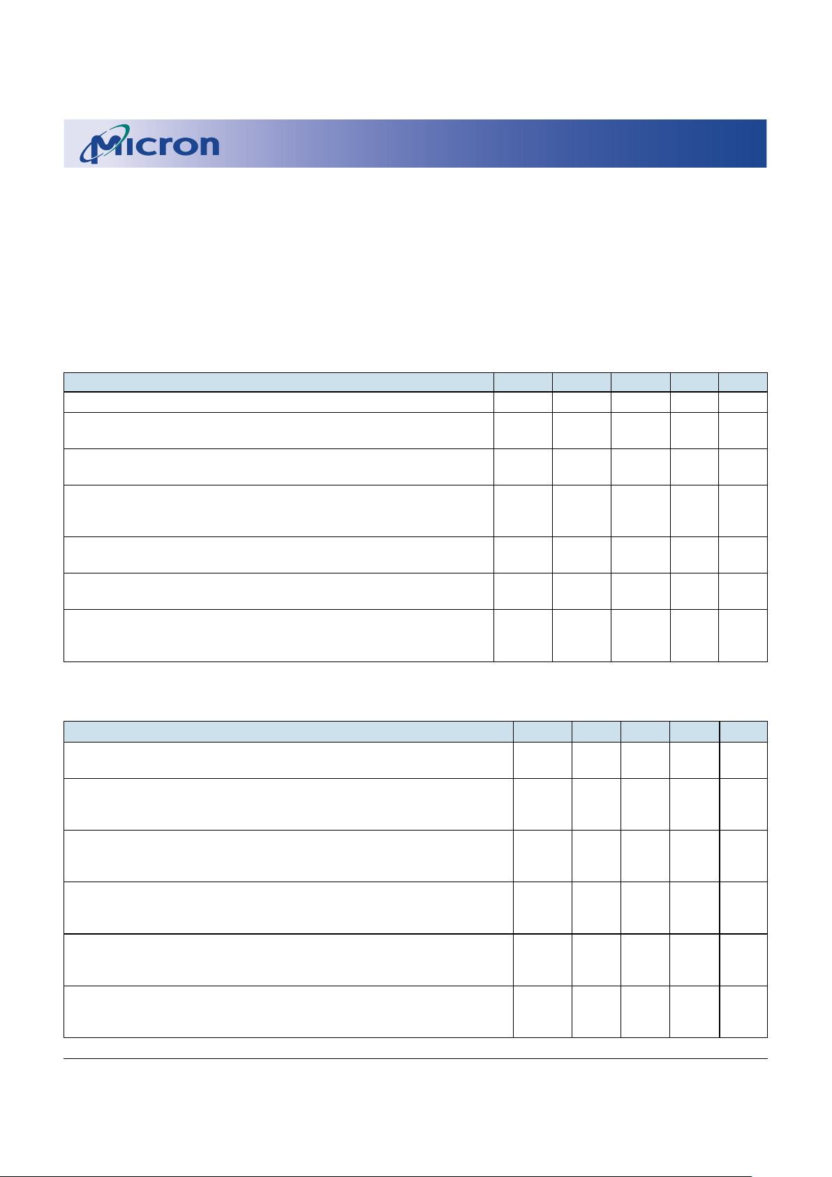
ABSOLUTE MAXIMUM RATINGS*
Voltage on VCC Relative to VSS ................-1V to +4.6V
Voltage on NC, Inputs or I/O Pins
Relative to VSS ....................................... -1V to +4.6V
Operating Temperature, TA (ambient) ... 0°C to +70°C
Storage Temperature (plastic) ............ -55°C to +150°C
Power Dissipation ................................................... 1W
*Stresses greater than those listed under “Absolute
Maximum Ratings” may cause permanent damage to
the device. This is a stress rating only, and functional
operation of the device at these or any other conditions
above those indicated in the operational sections of
this specification is not implied. Exposure to absolute
maximum rating conditions for extended periods may
affect reliability.
DC ELECTRICAL CHARACTERISTICS AND OPERATING CONDITIONS
(Notes: 1, 5, 6) (VCC = +3.3V ±0.3V)
PARAMETER/CONDITION SYMBOL MIN MAX UNITS NOTES
SUPPLY VOLTAGE VCC 3 3.6 V
INPUT HIGH VOLTAGE:
Valid Logic 1; All inputs, I/Os and any NC VIH 2VCC + 0.3 V 37
INPUT LOW VOLTAGE:
Valid Logic 0; All inputs, I/Os and any NC VIL -0.3 0.8 V 37
INPUT LEAKAGE CURRENT:
Any input at VIN (0V £ VIN £ VCC + 0.3V); II -2 2 µA
All other pins not under test = 0V
OUTPUT HIGH VOLTAGE:
IOUT = -2mA VOH 2.4–V
OUTPUT LOW VOLTAGE:
IOUT = 2mA VOL – 0.4 V
OUTPUT LEAKAGE CURRENT:
Any output at VOUT (0V £ VOUT £ VCC + 0.3V); IOZ -5 5 µA
DQ is disabled and in High-Z state
IDD OPERATING CONDITIONS AND MAXIMUM LIMITS
(Notes: 1, 2, 3, 5, 6) (VCC = +3.3V ±0.3V)
PARAMETER/CONDITION SYMBOL SPEED MAX UNITS NOTES
STANDBY CURRENT: TTL IDD1 ALL 1 mA
(RAS# = CAS# = VIH)
STANDBY CURRENT: CMOS
(RAS# = CAS# ³ VCC - 0.2V; DQs may be left open; IDD2 ALL 500 µA
Other inputs: VIN ³ VCC - 0.2V or VIN £ 0.2V)
OPERATING CURRENT: Random READ/WRITE -5 150
Average power supply current IDD3 -6 165 mA 25
(RAS#, CAS#, address cycling: tRC = tRC [MIN])
OPERATING CURRENT: FAST PAGE MODE -5 105
Average power supply current (RAS# = VIL,IDD4 -6 95 mA 25
CAS#, address cycling: tPC = tPC [MIN])
REFRESH CURRENT: RAS# ONLY -5 150
Average power supply current IDD5 -6 165 mA 22
(RAS# cycling, CAS# = VIH: tRC = tRC [MIN])
REFRESH CURRENT: CBR -5 150
Average power supply current IDD6 -6 165 mA 4, 7
(RAS#, CAS#, address cycling: tRC = tRC [MIN])
6
4 Meg x 16 FPM DRAM Micron Technology, Inc., reserves the right to change products or specifications without notice.
D28_2.p65 – Rev. 5/00 ©2000, Micron Technology, Inc.
4 MEG x 16
FPM DRAM
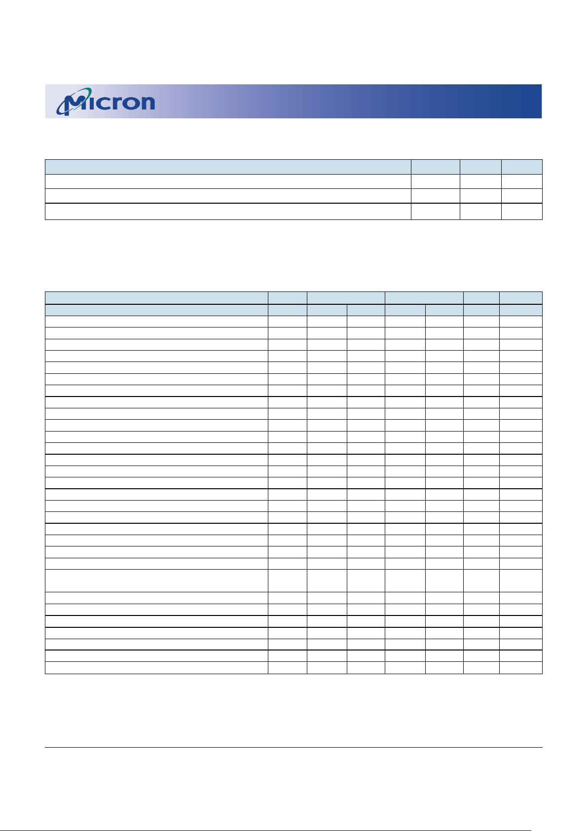
AC ELECTRICAL CHARACTERISTICS
(Notes: 5, 6, 7, 8, 9, 10, 11, 12, 13) (VCC = +3.3V ±0.3V)
AC CHARACTERISTICS -5 -6
PARAMETER SYMBOL MIN MAX MIN MAX UNITS NOTES
Access time from column address
t
AA 25 30 ns
Column-address hold time (referenced to RAS#)
t
AR 40 45 ns
Column-address setup time
t
ASC 0 0 ns 26
Row-address setup time
t
ASR 0 0 ns
Column address to WE# delay time
t
AWD 48 55 ns 18
Access time from CAS#
t
CAC 13 15 ns 28
Column-address hold time
t
CAH 8 10 ns 26
CAS# pulse width
t
CAS 13 10,000 15 10,000 ns 32, 34
CAS# hold time (CBR Refresh)
t
CHR 15 15 ns 4, 27
Last CAS# going LOW to first CAS# to return HIGH
t
CLCH 5 5 ns 29
CAS# to output in Low-Z
t
CLZ 3 3 ns 26, 28
CAS# precharge time (FAST PAGE MODE)
t
CP 8 10 ns 13, 32
Access time from CAS# precharge
t
CPA 30 35 ns 27
CAS# to RAS# precharge time
t
CRP 5 5 ns 27
CAS# hold time
t
CSH 50 60 ns 27
CAS# setup time (CBR Refresh)
t
CSR 5 5 ns 4, 26
CAS# to WE# delay time
t
CWD 36 40 ns 18, 26
WRITE command to CAS# lead time
t
CWL 13 15 ns 28
Data-in hold time
t
DH 8 10 ns 19, 28
Data-in setup time
t
DS 0 0 ns 19, 28
Output disable
t
OD 3 13 3 15 ns 23, 24, 36
Output enable time
t
OE 13 15 ns 20
OE# hold time from WE# during
t
OEH 13 15 ns 24
READ-MODIFY-WRITE cycle
Output buffer turn-off delay
t
OFF 3 13 3 15 ns 17, 23, 28
OE# setup prior to RAS# during HIDDEN REFRESH cycle
t
ORD 0 0 ns
FAST-PAGE-MODE READ or WRITE cycle time
t
PC 30 35 ns 30
FAST-PAGE-MODE READ-WRITE cycle time
t
PRWC 76 85 ns 30
Access time from RAS#
t
RAC 50 60 ns
RAS# to column-address delay time
t
RAD 13 15 ns 15
Row-address hold time
t
RAH 8 10 ns
CAPACITANCE
(Note: 2)
PARAMETER SYMBOL M AX UNITS
Input Capacitance: Address pins CI1 5pF
Input Capacitance: RAS#, CAS#, WE#, OE# CI2 7pF
Input/Output Capacitance: DQ CIO 7pF
 Loading...