

MICRON MT4LC1M16E5DJ-6, MT4LC1M16E5DJ-6S, MT4LC1M16E5DJ-5, MT4LC1M16E5DJ-, MT4C1M16E5DJ-5 Datasheet
...
1
1 Meg x 16 EDO DRAM
D52_B.p65 – Rev. B; Pub. 3/01 ©2001, Micron Technology, Inc
16Mb: 1 MEG x16
EDO DRAM
PRODUCTS AND SPECIFICATIONS DISCUSSED HEREIN ARE SUBJECT TO CHANGE BY MICRON WITHOUT NOTICE.
KEY TIMING PARAMETERS
SPEEDtRC
t
RAC
t
PC
t
AAtCACtCAS
-5 84ns 50ns 20ns 25ns 15ns 8ns
-6 104ns 60ns 25ns 30ns 17ns 10ns
FEATURES
• JEDEC- and industry-standard x16 timing,
functions, pinouts, and packages
• High-performance CMOS silicon-gate process
• Single power supply (+3.3V ±0.3V or 5V ±10%)
• All inputs, outputs and clocks are TTL-compatible
• Refresh modes: RAS#-ONLY, CAS#-BEFORE-RAS#
(CBR), HIDDEN; optional self refresh (S)
• BYTE WRITE access cycles
• 1,024-cycle refresh (10 row, 10 column addresses)
• Extended Data-Out (EDO) PAGE MODE access
• 5V-tolerant inputs and I/Os on 3.3V devices
OPTIONS MARKING
• Voltages
1
3.3V LC
5V C
• Refresh Addressing
1,024 (1K) rows E 5
• Packages
Plastic SOJ (400 mil) D J
Plastic TSOP (400 mil) TG
• Timing
50ns access -5
60ns access -6
• Refresh Rates
Standard Refresh (16ms period) None
Self Refresh (128ms period) S
2
• Operating Temperature Range
Commercial (0oC to +70oC) None
Extended (-20oC to +80oC) ET
Part Number Example:
MT4LC1M16E5TG-6
NOTE: 1. The third field distinguishes the low voltage offering: LC desig-
nates Vcc = 3.3V and C designates Vcc = 5V.
2. Available only on MT4LC1M16E5 (3.3V)
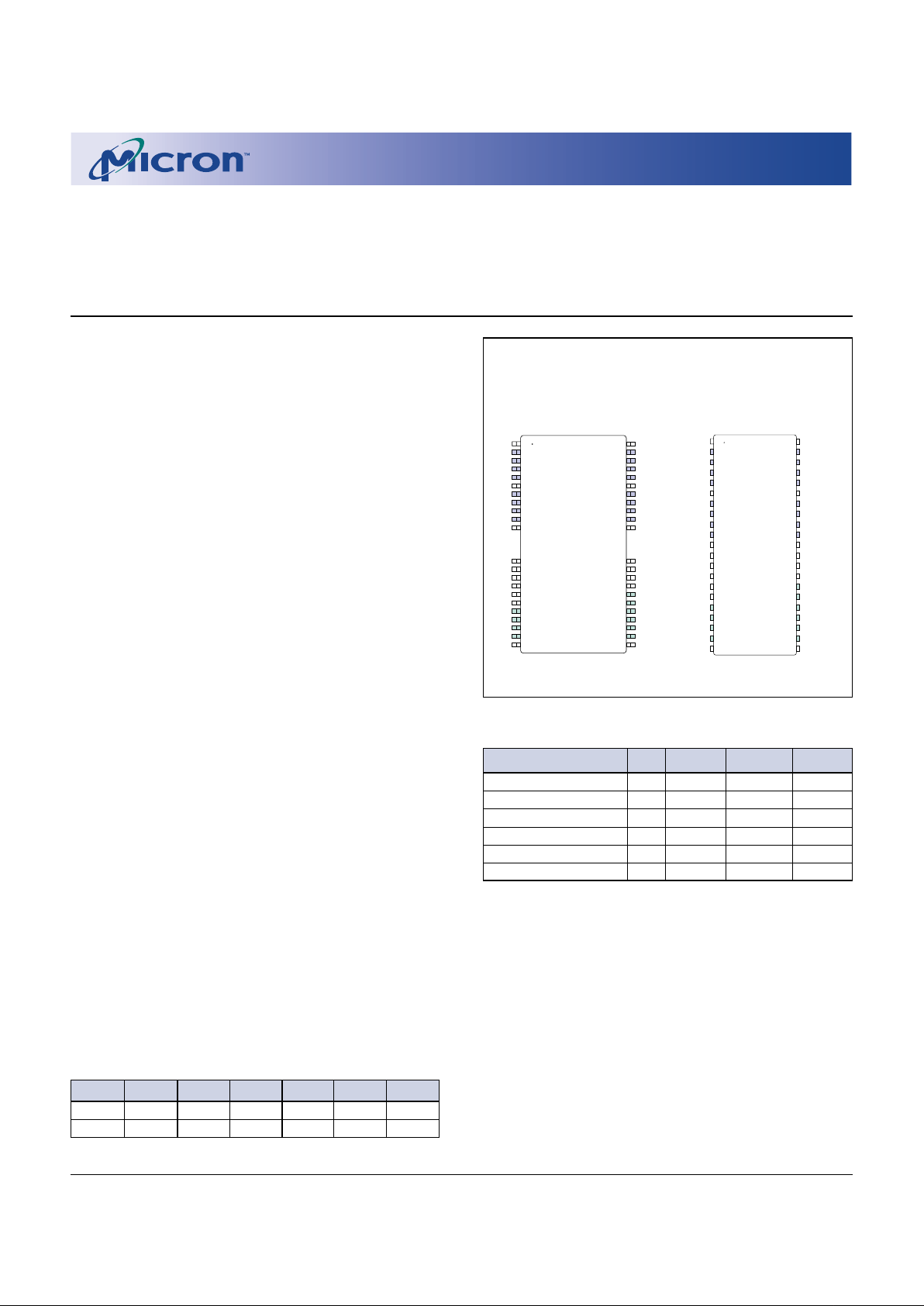
PIN ASSIGNMENT (Top View)
44/50-Pin TSOP 42-Pin SOJ
1 MEG x 16 EDO DRAM PART NUMBERS
PART NUMBER Vcc REFRESH PACKAGE REFRESH
MT4LC1M16E5DJ-x 3.3V 1K 400-SOJ Standard
MT4LC1M16E5DJ-x S 3.3V 1K 400-SOJ Self
MT4LC1M16E5TG-x 3.3V 1K 400-TSOP Standard
MT4LC1M16E5TG-x S 3.3V 1K 400-TSOP Self
MT4C1M16E5DJ-x 5V 1K 400-SOJ Standard
MT4C1M16E5TG-x 5V 1K 400-TSOP Standard
NOTE: “-x” indicates speed grade marking under timing
options.
EDO DRAM
MT4C1M16E5 – 1 Meg x 16, 5V
MT4LC1M16E5 – 1 Meg x 16, 3.3V
For the latest data sheet, please refer to the Micron Web
site: www.micron.com/products/datasheets/sdramds.html
NOTE: The "#" symbol indicates signal is active LOW.
V
CC
DQ0
DQ1
DQ2
DQ3
V
CC
DQ4
DQ5
DQ6
DQ7
NC
NC
NC
WE#
RAS#
NC
NC
A0
A1
A2
A3
V
CC
1
2
3
4
5
6
7
8
9
10
11
15
16
17
18
19
20
21
22
23
24
25
50
49
48
47
46
45
44
43
42
41
40
36
35
34
33
32
31
30
29
28
27
26
V
SS
DQ15
DQ14
DQ13
DQ12
V
SS
DQ11
DQ10
DQ9
DQ8
NC
NC
CASL#
CASH#
OE#
A9
A8
A7
A6
A5
A4
V
SS
VCC
DQ0
DQ1
DQ2
DQ3
V
CC
DQ4
DQ5
DQ6
DQ7
NC
NC
WE#
RAS#
NC
NC
A0
A1
A2
A3
V
CC
1
2
3
4
5
6
7
8
9
10
11
12
13
14
15
16
17
18
19
20
21
42
41
40
39
38
37
36
35
34
33
32
31
30
29
28
27
26
25
24
23
22
V
SS
DQ15
DQ14
DQ13
DQ12
V
SS
DQ11
DQ10
DQ9
DQ8
NC
CASL#
CASH#
OE#
A9
A8
A7
A6
A5
A4
V
SS
GENERAL DESCRIPTION
The 1 Meg x 16 is a randomly accessed, solid-state
memory containing 16,777,216 bits organized in a x16
configuration. The 1 Meg x 16 has both BYTE WRITE
and WORD WRITE access cycles via two CAS# pins
(CASL# and CASH#). These function like a single CAS#
found on other DRAMs in that either CASL# or CASH#
will generate an internal CAS#.
The CAS# function and timing are determined by
the first CAS# (CASL# or CASH#) to transition LOW and
the last CAS# to transition back HIGH. Using only one
2
1 Meg x 16 EDO DRAM Micron Technology, Inc., reserves the right to change products or specifications without notice.
D52_B.p65 – Rev. B; Pub. 3/01 ©2001, Micron Technology, Inc
16Mb: 1 MEG x16
EDO DRAM
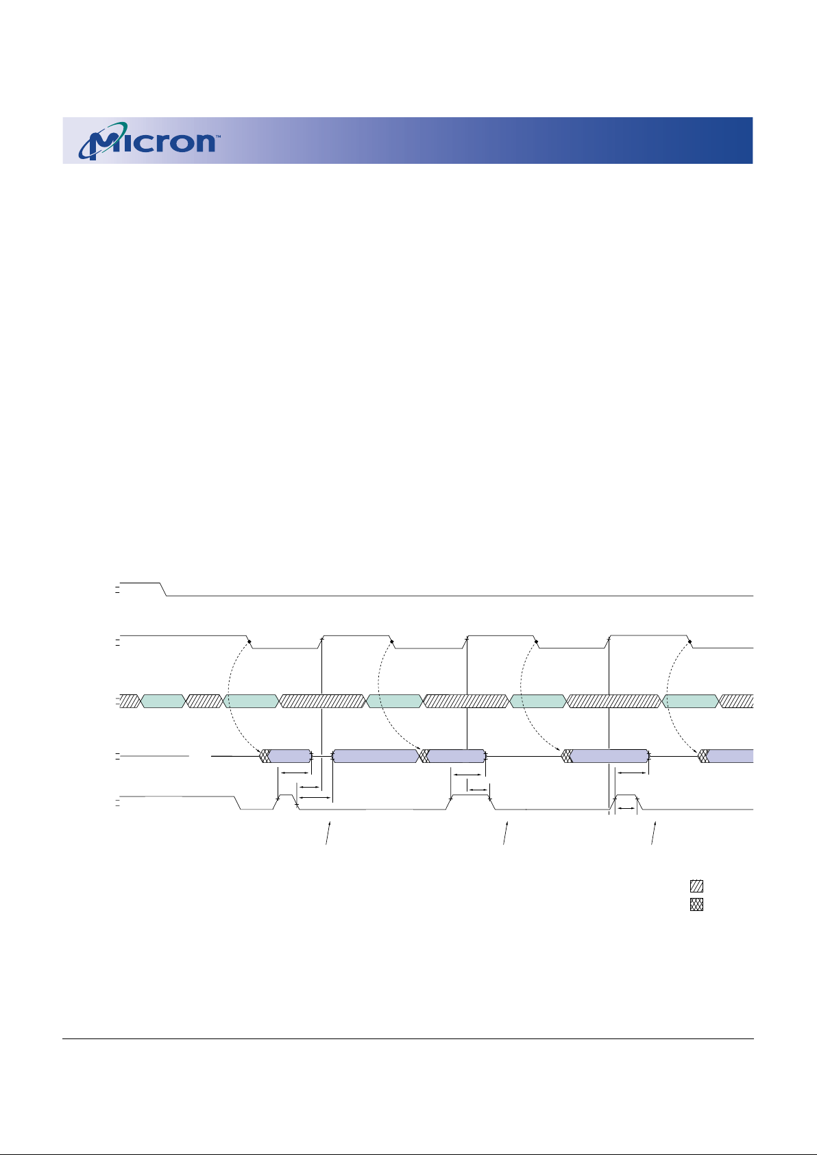
Figure 1
OE# Control of DQs
V
V
IH
IL
CASL#/CASH#
V
V
IH
IL
RAS#
V
V
IH
IL
ADDR
ROW COLUMN (A)
COLUMN (B)
DON’T CARE
UNDEFINED
V
V
IH
IL
OE#
V
V
IOH
IOL
OPEN
DQ
t
OD
VALID DATA (B)
VALID DATA (A)
COLUMN (C)
VALID DATA (A)
t
OE
VALID DATA (C)
COLUMN (D)
VALID DATA (D)
t
OD
t
OEHC
t
OD
t
OEP
t
OES
The DQs go back to
Low-Z if
t
OES is met.
The DQs remain High-Z
until the next CAS# cycle
if
t
OEHC is met.
The DQs remain High-Z
until the next CAS# cycle
if
t
OEP is met.
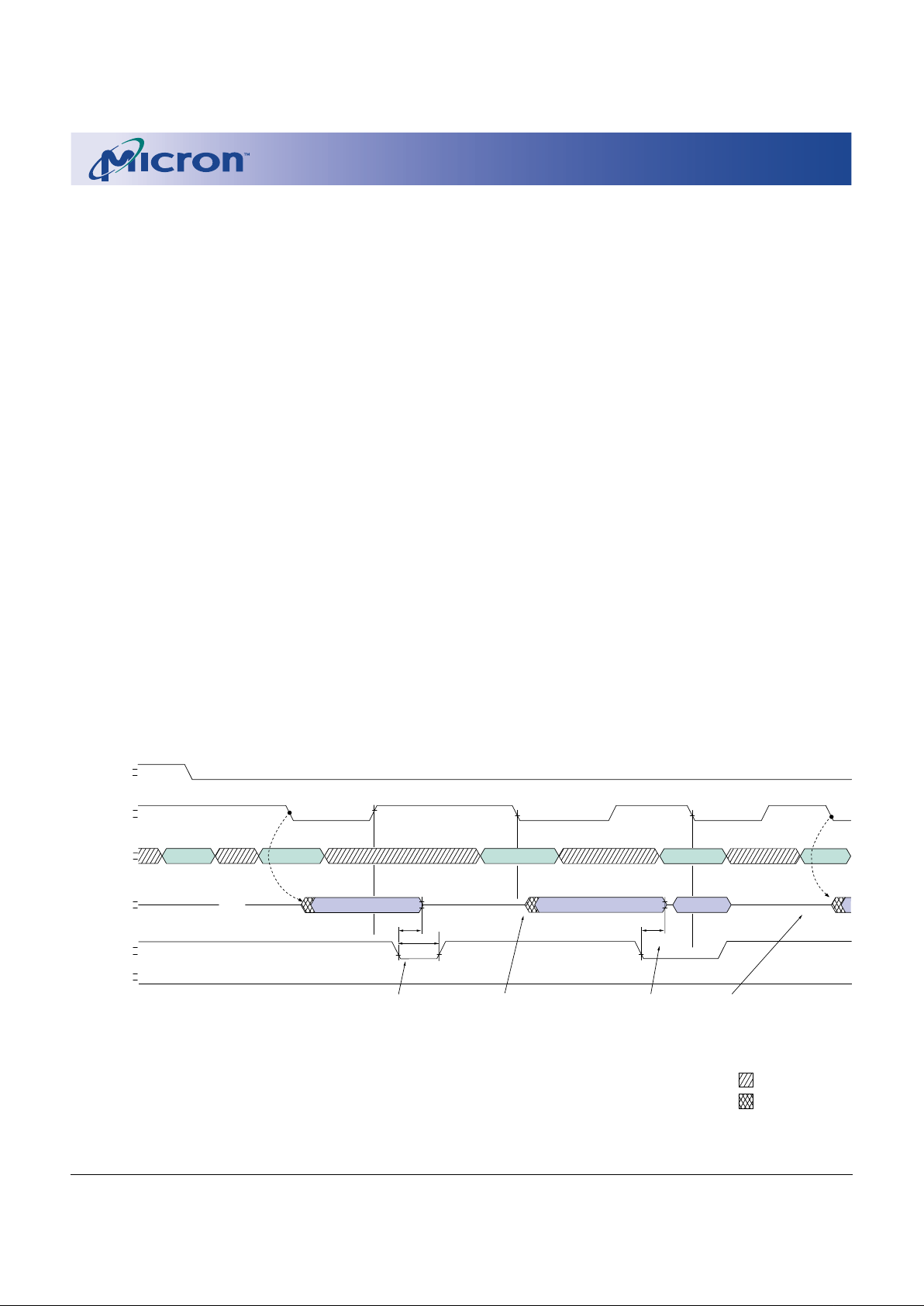
A logic HIGH on WE# dictates read mode, while a
logic LOW on WE# dictates write mode. During a WRITE
cycle, data-in (D) is latched by the falling edge of WE or
CAS# (CASL# or CASH#), whichever occurs last. An
EARLY WRITE occurs when WE is taken LOW prior to
either CAS# falling. A LATE WRITE or READ-MODIFYWRITE occurs when WE falls after CAS# (CASL# or
CASH#) was taken LOW. During EARLY WRITE cycles,
the data outputs (Q) will remain High-Z, regardless of
the state of OE#. During LATE WRITE or READMODIFY-WRITE cycles, OE# must be taken HIGH to
disable the data outputs prior to applying input data.
If a LATE WRITE or READ-MODIFY-WRITE is attempted
while keeping OE# LOW, no WRITE will occur, and the
data outputs will drive read data from the accessed
location.
The 16 data inputs and 16 data outputs are routed
through 16 pins using common I/O. Pin direction is
controlled by OE# and WE#.
The 1 Meg x 16 DRAM must be refreshed periodically in order to retain stored data.
of the two signals results in a BYTE WRITE cycle. CASL#
transitioning LOW selects an access cycle for the lower
byte (DQ0-DQ7), and CASH# transitioning LOW selects an access cycle for the upper byte (DQ8-DQ15).
Each bit is uniquely addressed through the 20 address bits during READ or WRITE cycles. These are
entered 10 bits (A0-A9) at a time. RAS# is used to latch
the first 10 bits and CAS#, the latter 10 bits. The CAS#
function also determines whether the cycle will be a
refresh cycle (RAS# ONLY) or an active cycle (READ,
WRITE or READ-WRITE) once RAS# goes LOW.
The CASL# and CASH# inputs internally generate a
CAS# signal that functions like the single CAS# input
on other DRAMs. The key difference is each CAS# input
(CASL# and CASH#) controls its corresponding eight
DQ inputs during WRITE accesses. CASL# controls
DQ0-DQ7, and CASH# controls DQ8-DQ15. The two
CAS# controls give the 1 Meg x 16 both BYTE READ and
BYTE WRITE cycle capabilities.
GENERAL DESCRIPTION (continued)
3
1 Meg x 16 EDO DRAM Micron Technology, Inc., reserves the right to change products or specifications without notice.
D52_B.p65 – Rev. B; Pub. 3/01 ©2001, Micron Technology, Inc
16Mb: 1 MEG x16
EDO DRAM
V
V
IH
IL
CASL#/CASH#
V
V
IH
IL
RAS#
V
V
IH
IL
ADDR
ROW COLUMN (A)
DON‘T CARE
UNDEFINED
V
V
IH
IL
WE#
V
V
IOH
IOL
OPEN
DQ
t
WPZ
The DQs go to High-Z if WE# falls, and if tWPZ is met,
will remain High-Z until CAS# goes LOW with
WE# HIGH (i.e., until a READ cycle is initiated).
V
V
IH
IL
OE#
VALID DATA (B)
t
WHZ
WE# may be used to disable the DQs to prepare
for input data in an EARLY WRITE cycle. The DQs
will remain High-Z until CAS# goes LOW with
WE# HIGH (i.e., until a READ cycle is initiated).
t
WHZ
COLUMN (D)
VALID DATA (A)
COLUMN (B)
COLUMN (C)
INPUT DATA (C)
Figure 2
WE# Control of DQs
PAGE ACCESS
Page operations allow faster data operations (READ,
WRITE or READ-MODIFY-WRITE) within a rowaddress-defined page boundary. The page cycle is always initiated with a row address strobed in by RAS#,
followed by a column address strobed in by CAS#. Additional columns may be accessed by providing valid
column addresses, strobing CAS# and holding RAS#
LOW, thus executing faster memory cycles. Returning
RAS# HIGH terminates the page mode of operation,
i.e., closes the page.
EDO PAGE MODE
The 1 Meg x 16 provides EDO PAGE MODE, which is
an accelerated FAST-PAGE-MODE cycle. The primary
advantage of EDO is the availability of data-out even
after CAS# returns HIGH. EDO provides for CAS#
precharge time (tCP) to occur without the output data
going invalid. This elimination of CAS# output control
provides for pipelined READs.
FAST-PAGE-MODE DRAMs have traditionally
turned the output buffers off (High-Z) with the rising
edge of CAS#. EDO-PAGE-MODE DRAMs operate like
FAST-PAGE-MODE DRAMs, except data will remain
valid or become valid after CAS# goes HIGH during
READs, provided RAS# and OE# are held LOW. If OE# is
pulsed while RAS# and CAS# are LOW, data will toggle
from valid data to High-Z and back to the same valid
data. If OE# is toggled or pulsed after CAS# goes HIGH
while RAS# remains LOW, data will transition to and
remain High-Z (refer to Figure 1). WE# can also perform
the function of disabling the output drivers under certain conditions, as shown in Figure 2.
During an application, if the DQ outputs are wire
OR’d, OE# must be used to disable idle banks of DRAMs.
Alternatively, pulsing WE# to the idle banks during
CAS# HIGH time will also High-Z the outputs. Independent of OE# control, the outputs will disable after
t
OFF, which is referenced from the rising edge of RAS#
or CAS#, whichever occurs last.
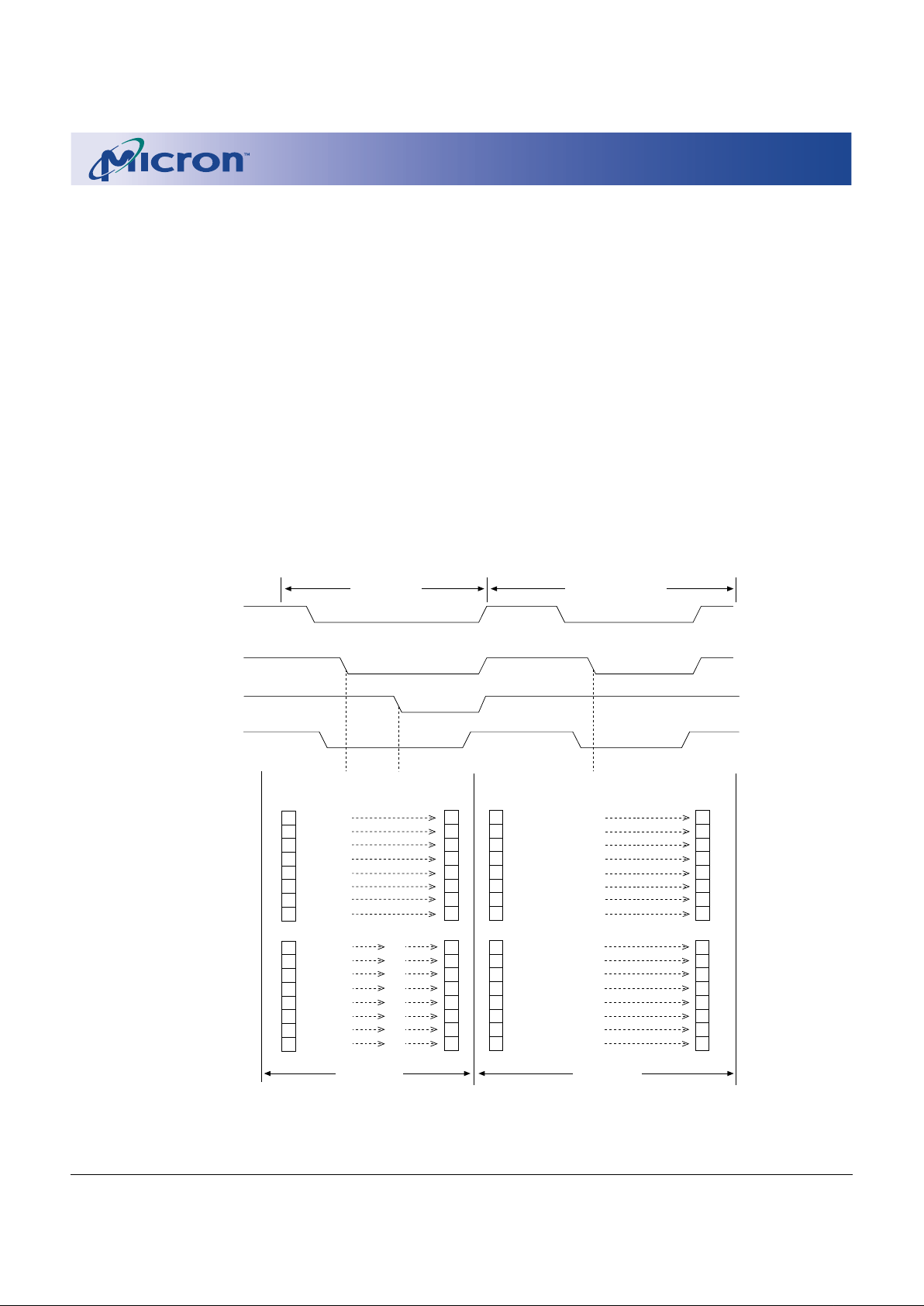
BYTE ACCESS CYCLE
The BYTE WRITEs and BYTE READs are determined
by the use of CASL# and CASH#. Enabling CASL# selects a lower BYTE access (DQ0-DQ7). Enabling CASH#
selects an upper BYTE access (DQ8-DQ15). Enabling
both CASL# and CASH# selects a WORD WRITE cycle.
The 1 Meg x 16 may be viewed as two 1 Meg x 8
DRAMs that have common input controls, with the exception of the CAS# inputs. Figure 3 illustrates the BYTE
WRITE and WORD WRITE cycles.
Additionally, both bytes must always be of the same
mode of operation if both bytes are active. A CAS#
precharge must be satisfied prior to changing modes of
operation between the upper and lower bytes. For example, an EARLY WRITE on one byte and a LATE WRITE
on the other byte are not allowed during the same cycle.
4
1 Meg x 16 EDO DRAM Micron Technology, Inc., reserves the right to change products or specifications without notice.
D52_B.p65 – Rev. B; Pub. 3/01 ©2001, Micron Technology, Inc
16Mb: 1 MEG x16
EDO DRAM
STORED
DATA
1
1
0
1
1
1
1
1
RAS#
CASL#
WE#
X = NOT EFFECTIVE (DON'T CARE)
ADDRESS 1ADDRESS 0
0
1
0
1
0
0
0
0
WORD WRITE LOWER BYTE WRITE
CASH#
INPUT
DATA
0
0
1
0
0
0
0
0
1
0
1
0
1
1
1
1
X
X
X
X
X
X
X
X
INPUT
DATA
1
1
0
1
1
1
1
1
INPUT
DATA
STORED
DATA
1
1
0
1
1
1
1
1
INPUT
DATA
STORED
DATA
0
0
1
0
0
0
0
0
1
0
1
0
1
1
1
1
STORED
DATA
0
0
1
0
0
0
0
0
1
0
1
0
1
1
1
1
X
X
X
X
X
X
X
X
1
0
1
0
1
1
1
1
UPPER BYTE
(DQ8-DQ15)
OF WORD
LOWER BYTE
(DQ0-DQ7)
OF WORD
Figure 3
WORD and BYTE WRITE Example
However, an EARLY WRITE on one byte and a LATE
WRITE on the other byte, after a CAS# precharge has
been satisfied, are permissible.
DRAM REFRESH
Preserve correct memory cell data by maintaining
power and executing any RAS# cycle (READ, WRITE) or
RAS# REFRESH cycle (RAS#-ONLY, CBR or HIDDEN)
so that all 1,024 combinations of RAS# addresses are
executed within tREF (MAX), regardless of sequence.
The CBR, EXTENDED and SELF REFRESH cycles will
invoke the internal refresh counter for automatic RAS#
addressing.
An optional self refresh mode is available on the “S”
version. The self refresh feature is initiated by performing a CBR REFRESH cycle and holding RAS# LOW
for the specified tRASS. The “S” option allows the user
the choice of a fully static, low-power data retention
mode or a dynamic refresh mode at the extended refresh period of 128ms, or 125µs per row, when using a
distributed CBR REFRESH. This refresh rate can be
applied during normal operation, as well as during a
standby or battery backup mode.
The self refresh mode is terminated by driving
RAS# HIGH for a minimum time of tRPS. This delay
allows for the completion of any internal refresh cycles
that may be in process at the time of the RAS# LOW-toHIGH transition. If the DRAM controller uses a distributed refresh sequence, a burst refresh is not required
upon exiting self refresh. However, if the DRAM controller utilizes a RAS#-ONLY or burst refresh sequence,
all 1,024 rows must be refreshed within the average
internal refresh rate, prior to the resumption of normal
operation.
STANDBY
Returning RAS# and CAS# HIGH terminates a
memory cycle and decreases chip current to a reduced
standby level. The chip is preconditioned for the next
cycle during the RAS# HIGH time.
5
1 Meg x 16 EDO DRAM Micron Technology, Inc., reserves the right to change products or specifications without notice.
D52_B.p65 – Rev. B; Pub. 3/01 ©2001, Micron Technology, Inc
16Mb: 1 MEG x16
EDO DRAM
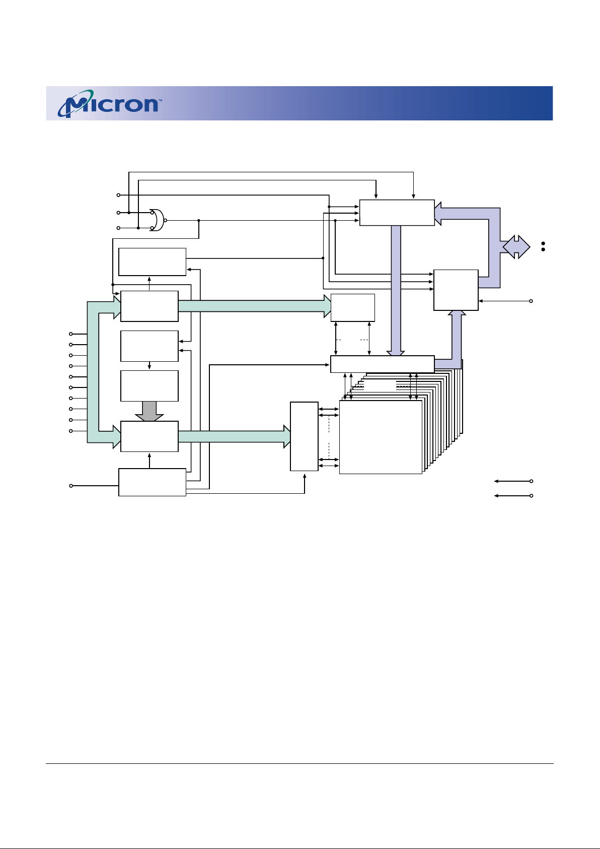
CASL#
CAS#
RAS#
10
10
NO. 2 CLOCK
GENERATOR
REFRESH
CONTROLLER
NO. 1 CLOCK
GENERATOR
1,024 x 1,024 x 16
MEMORY
ARRAY
V
DD
V
SS
10
OE#
DQ0
DQ15
REFRESH
COUNTER
CASH#
A0
A1
A2
A3
A4
A5
A6
A7
A8
A9
1,024
1,024 x 16
16
10
10
SENSE AMPLIFIERS
I/O GATING
1,024
DATA-OUT
BUFFER
WE#
16
ROW-
ADDRESS
BUFFERS (10)
ROW
DECODER
COLUMN-
ADDRESS
BUFFER
DATA-IN BUFFER
COLUMN
DECODER
16
FUNCTIONAL BLOCK DIAGRAM
6
1 Meg x 16 EDO DRAM Micron Technology, Inc., reserves the right to change products or specifications without notice.
D52_B.p65 – Rev. B; Pub. 3/01 ©2001, Micron Technology, Inc
16Mb: 1 MEG x16
EDO DRAM
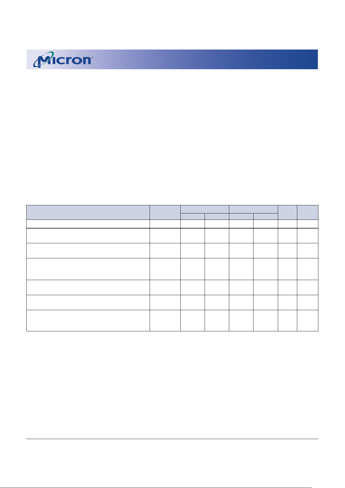
DC ELECTRICAL CHARACTERISTICS AND OPERATING CONDITIONS
(Notes: 1; notes appear on pages 10-11)
3.3V 5V
PARAMETER/CONDITION SYMBOL MIN MAX MIN M AX UNITS NOTES
SUPPLY VOLTAGE VCC 3.0 3.6 4.5 5.5 V
INPUT HIGH VOLTAGE:
Valid Logic 1; All inputs, I/Os and any NC VIH 2.0 5.5 2.4 VCC + 1 V
INPUT LOW VOLTAGE:
Valid Logic 0; All inputs, I/Os and any NC VIL -1.0 0.8 -0.5 0.8 V
INPUT LEAKAGE CURRENT:
Any input at VIN (0V £ VIN £ VIH[MAX]); II -2 2 -2 2 µ A 4
All other pins not under test = 0V
OUTPUT HIGH VOLTAGE:
IOUT = -2mA(3.3V), -5mA(5V) VOH 2.4 – 2.4 – V
OUTPUT LOW VOLTAGE:
IOUT = 2mA(3.3V), 4.2mA(5V) VOL – 0.4 – 0.4 V
OUTPUT LEAKAGE CURRENT:
Any output at VOUT (0V £ VOUT £ 5.5V); IOZ -5 5 -5 5 µA
DQ is disabled and in High-Z state
ABSOLUTE MAXIMUM RATINGS*
Voltage on VCC Pin Relative to VSS
3.3V ......................................................... -1V to +4.6V
5V ............................................................... -1V to +7V
Voltage on NC, Inputs or I/O Pins Relative to Vss:
3.3V ......................................................... -1V to +5.5V
5V ............................................................... -1V to +7V
Operating Temperature
TA (commercial) .................................. 0ºC to +70ºC
TA (extended)................................... -20ºC to +80ºC
Storage Temperature (plastic) ........... -55ºC to +150ºC
Power Dissipation ........................................................ 1W
Short Circuit Output Current ................................ 50mA
*Stresses greater than those listed under “Absolute
Maximum Ratings” may cause permanent damage to
the device. This is a stress rating only, and functional
operation of the device at these or any other conditions
above those indicated in the operational sections of
this specification is not implied. Exposure to absolute
maximum rating conditions for extended periods may
affect reliability.
7
1 Meg x 16 EDO DRAM Micron Technology, Inc., reserves the right to change products or specifications without notice.
D52_B.p65 – Rev. B; Pub. 3/01 ©2001, Micron Technology, Inc
16Mb: 1 MEG x16
EDO DRAM
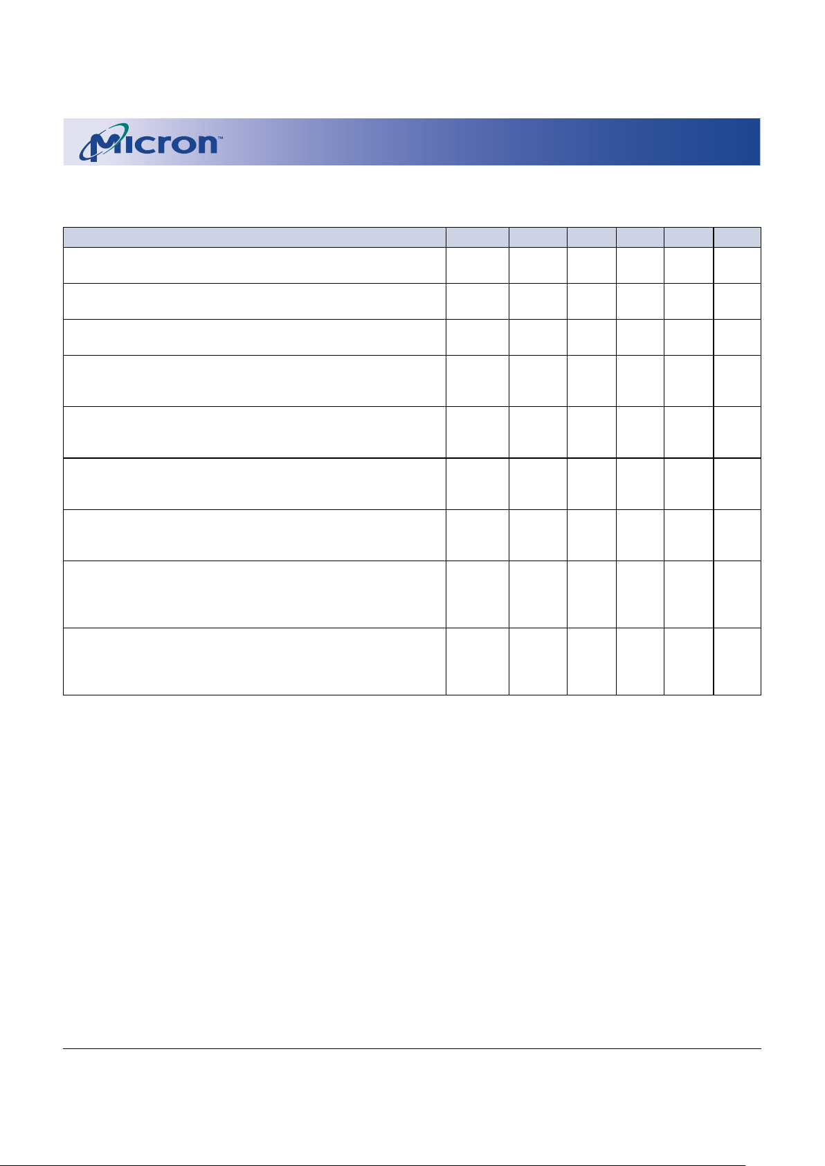
ICC OPERATING CONDITIONS AND MAXIMUM LIMITS
(Notes: 1, 2, 3, 5, 8; notes appear on pages 10-11); (VCC[MIN] £ VCC £ VCC[MAX])
PARAMETER/CONDITION SYMBOL SPEED 3.3V 5V UNITS NOTES
STANDBY CURRENT: TTL ICC1 ALL 1 2 mA
(RAS# = CAS# = VIH)
STANDBY CURRENT: CMOS (non-“S” version only) ICC2 ALL 500 500 µA
(RAS# = CAS# = other inputs = VDD - 0.2V)
STANDBY CURRENT: CMOS (“S” version only) ICC2 ALL 150 150 µA
(RAS# = CAS# = other inputs = VDD - 0.2V)
OPERATING CURRENT: Random READ/WRITE ICC3 -5 180 190 m A 6
Average power supply current -6 170 180
(RAS#, CAS#, address cycling: tRC = tRC [MIN])
OPERATING CURRENT: EDO PAGE MODE ICC4 -5 140 150 mA 6
Average power supply current (RAS# = VIL, CAS#, -6 130 140
address cycling: tPC = tPC [MIN])
REFRESH CURRENT: RAS#-ONLY ICC5 -5 180 190 mA
Average power supply current -6 170 180
(RAS# cycling, CAS# = VIH: tRC = tRC [MIN])
REFRESH CURRENT: CBR ICC6 -5 180 180 mA 7, 9
Average power supply current -6 170 170
(RAS#, CAS#, address cycling: tRC = tRC [MIN])
REFRESH CURRENT: Extended (“S” version only) ICC7 ALL 300 300 µA 7, 9
Average power supply current: CAS# = 0.2V or CBR cycling;
RAS# = tRAS (MIN); WE# = VDD - 0.2V; A0-A10, OE# and
DIN = VDD - 0.2V or 0.2V (DIN may be left open); tRC = 125µs
REFRESH CURRENT: Self (“S” version only) ICC8 ALL 300 300 µA 7, 9
Average power supply current: CBR with RAS# tRASS (MIN)
and CAS# held LOW; WE# = VDD - 0.2V; A0-A10,
OE# and DIN = VDD - 0.2V or 0.2V (DIN may be left open)
8
1 Meg x 16 EDO DRAM Micron Technology, Inc., reserves the right to change products or specifications without notice.
D52_B.p65 – Rev. B; Pub. 3/01 ©2001, Micron Technology, Inc
16Mb: 1 MEG x16
EDO DRAM
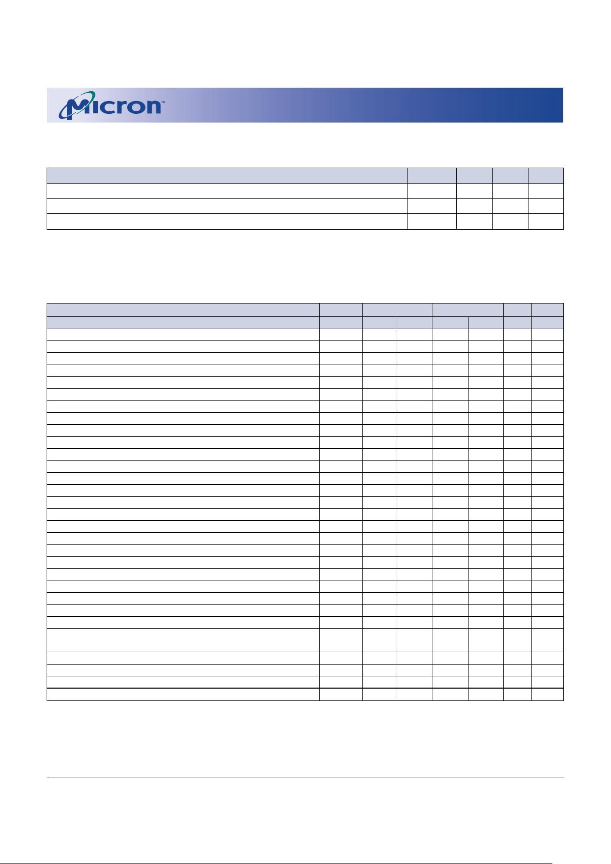
CAPACITANCE
(Notes: 1, 2, 3, 5, 8; notes appear on pages 10-11)
PARAMETER SYMBOL MAX UNITS NOTES
Input Capacitance: Addresses CI1 5pF
Input Capacitance: RAS#, CASL#,CASH#, WE#, OE# CI2 7pF
Input/Output Capacitance: DQ CIO 7pF
AC ELECTRICAL CHARACTERISTICS
(Notes: 2, 3, 9, 10, 11, 12; notes appear on pages 10-11); (VCC[MIN] £ VCC £ VCC[MAX])
AC CHARACTERISTICS -5 -6
PARAMETER SYMBOL MIN MAX MIN MAX UNITS NOTES
Access time from column address
t
AA 25 30 ns
Column-address setup to CAS# precharge
t
ACH 12 15 ns
Column-address hold time (referenced to RAS#)
t
AR 38 45 ns
Column-address setup time
t
ASC 0 0 ns 25
Row-address setup time
t
ASR 0 0 ns 25
Column address to WE# delay time
t
AWD 42 49 ns 13
Access time from CAS#
t
CAC 13 15 ns 14, 25
Column-address hold time
t
CAH 8 10 ns 25
CAS# pulse width
t
CAS 8 10,000 10 10,000 ns 27
CAS# LOW to “Don’t Care” during Self Refresh
t
CHD 15 15 ns
CAS# hold time (CBR Refresh)
t
CHR 8 10 ns 7, 26
Last CAS# going LOW to first CAS# to return HIGH
t
CLCH 5 5 ns 28
CAS# to output in Low-Z
t
CLZ 0 0 ns 26
Data output hold after next CAS# LOW
t
COH 3 3 ns
CAS# precharge time
t
CP 8 10 ns 15, 30
Access time from CAS# precharge
t
CPA 28 35 ns 26
CAS# to RAS# precharge time
t
CRP 5 5 ns 26
CAS# hold time
t
CSH 38 45 ns 26
CAS# setup time (CBR Refresh)
t
CSR 5 5 ns 7, 25
CAS# to WE# delay time
t
CWD 28 35 ns 13, 25
WRITE command to CAS# lead time
t
CWL 8 10 ns 26
Data-in hold time
t
DH 8 10 ns 16, 25
Data-in setup time
t
DS 0 0 ns 16, 25
Output disable
t
OD 0 12 0 15 ns
Output enable
t
OE 12 15 ns 17
OE# hold time from WE# during
t
OEH 8 10 ns 18
READ-MODIFY-WRITE cycle
OE# HIGH hold from CAS# HIGH
t
OEHC 5 10 ns 18
OE# HIGH pulse width
t
OEP 5 5 ns
OE# LOW to CAS# HIGH setup time
t
OES 4 5 ns
Output buffer turn-off delay
t
OFF 0 12 0 15 ns 20, 26
 Loading...