

MICRON MT48LC4M8A1TG-10, MT48LC4M4A1TG-8B Datasheet
PRODUCTS AND SPECIFICATIONS DISCUSSED HEREIN ARE SUBJECT TO CHANGE BY MICRON WITHOUT NOTICE.
1
16 Meg: x4, x8 SDRAM ©1998, Micron Technology, Inc.
16MSDRAMx4x8_B.p65 – Rev. 5/98
16 MEG: x4, x8
SDRAM
16Mb (x4/x8) SDRAM PART NUMBERS
PART NUMBER ARCHITECTURE
MT48LC4M4A1TG S 4 Meg x 4 (tWR = 1 CLK)
MT48LC2M8A1TG S 2 Meg x 8 (
t
WR = 1 CLK)
4 MEG x 4 2 MEG x 8
Configuration 2 Meg x 4 x 2 banks 1 Meg x 8 x 2 banks
Refresh Count 4K 4K
Row Addressing 2K (A0-A10) 2K (A0-A10)
Bank Addressing 2 (BA) 1 (BA)
Column Addressing 1K (A0-A9) 512 (A0-A8)
FEATURES
• PC100-compliant; includes CONCURRENT AUTO
PRECHARGE
• Fully synchronous; all signals registered on positive
edge of system clock
• Internal pipelined operation; column address can be
changed every clock cycle
• Internal banks for hiding row access/precharge
• Programmable burst lengths: 1, 2, 4, 8, or full page
• Auto Precharge and Auto Refresh Modes
• Self Refresh Mode
• 64ms, 4,096-cycle refresh
• LVTTL-compatible inputs and outputs
• Single +3.3V ±0.3V power supply
• Longer lead TSOP for improved reliability (OCPL*)
• One- and two-clock WRITE recovery (tWR) versions
OPTIONS MARKING
• Configurations
4 Meg x 4 (2 Meg x 4 x 2 banks) 4M4
2 Meg x 8 (1 Meg x 8 x 2 banks) 2M8
• WRITE Recovery (tWR/tDPL)
t
WR = 1 CLK A1
t
WR = 2 CLK (Contact factory for availability.)A2
• Plastic Package - OCPL*
44-pin TSOP (400 mil) TG
• Timing (Cycle Time)
8ns; tAC = 6ns @ CL = 3 -8B
10ns; tAC = 9ns @ CL = 2 -10
NOTE: The 16Mb SDRAM base number differentiates the
offerings in two places: MT48LC2M8A1 S. The fourth
field distinguishes the architecture offering: 4M4
designates 4 Meg x 4, and 2M8 designates 2 Meg x 8.
The fifth field distinguishes the WRITE recovery
offering: A1 designates one CLK and A2 designates two
CLKs.
Part Number Example:
MT48LC2M8A1TG-10 S
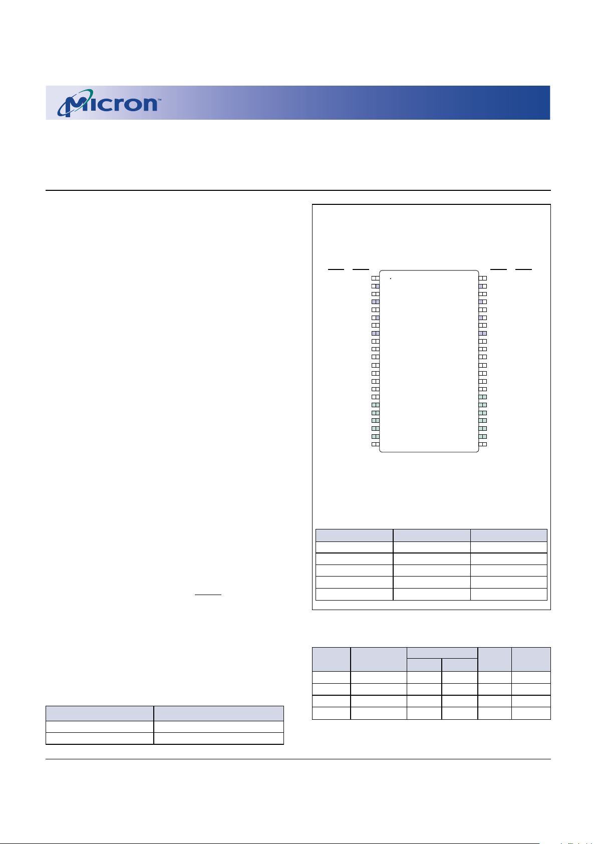
PIN ASSIGNMENT (Top View)
44-Pin TSOP
VDD
DQ0
VssQ
DQ1
V
DDQ
DQ2
VssQ
DQ3
V
DDQ
NC
NC
WE#
CAS#
RAS#
CS#
BA
A10
A0
A1
A2
A3
V
DD
1
2
3
4
5
6
7
8
9
10
11
12
13
14
15
16
17
18
19
20
21
22
44
43
42
41
40
39
38
37
36
35
34
33
32
31
30
29
28
27
26
25
24
23
Vss
DQ7
VssQ
DQ6
V
DDQ
DQ5
VssQ
DQ4
V
DDQ
NC
NC
DQM
CLK
CKE
NC
A9
A8
A7
A6
A5
A4
Vss
-
NC
-
DQ0
-
NC
-
DQ1
-
-
-
-
-
-
-
-
-
-
-
-
-
-
-
NC
-
DQ3
-
NC
-
DQ2
-
-
-
-
-
-
-
-
-
-
-
-
-
-
x4x8 x8x4
NOTE: The # symbol indicates signal is active LOW. A dash
(-) indicates x4 pin function is same as x8 pin
function.
SYNCHRONOUS
DRAM
MT48LC4M4A1/A2 S - 2 Meg x 4 x 2 banks
MT48LC2M8A1/A2 S - 1 Meg x 8 x 2 banks
For the latest data sheet revisions, please refer to the
Micron Web site: www.micron.com/datasheets.
KEY TIMING PARAMETERS
SPEED CLOCK ACCESS TIME SETUP HOLD
GRADE FREQUENCY CL = 2** CL = 3** TIME TIME
-8B 125 MHz – 6ns 2ns 1ns
-10 100 MHz – 7.5ns 3ns 1ns
-8B 83 MHz 9ns – 2ns 1ns
-10 66 MHz 9ns – 3ns 1ns
* Off-center parting line
**CL = CAS (READ) latency

2
16 Meg: x4, x8 SDRAM Micron Technology, Inc., reserves the right to change products or specifications without notice.
16MSDRAMx4x8_B.p65 – Rev. 5/98 ©1998, Micron Technology, Inc.
16 MEG: x4, x8
SDRAM
GENERAL DESCRIPTION
The Micron 16Mb SDRAM is a high-speed CMOS,
dynamic random-access memory containing 16,777,216
bits. It is internally configured as a dual memory array
(the 4 Meg x 4 is a dual 2 Meg x 4, and the 2 Meg x 8 is a dual
1 Meg x 8) with a synchronous interface (all signals are
registered on the positive edge of the clock signal, CLK).
Each of the two internal banks is organized with 2,048
rows and either 1,024 columns by 4 bits (4 Meg x 4) or 512
columns by 8 bits (2 Meg x 8).
Read and write accesses to the SDRAM are burst oriented; accesses start at a selected location and continue
for a programmed number of locations in a programmed
sequence. Accesses begin with the registration of an ACTIVE command, which is then followed by a READ or
WRITE command. The address bits registered coincident with the ACTIVE command are used to select the
bank and row to be accessed (BA selects the bank, A0-A10
select the row). The address bits registered coincident
with the READ or WRITE command are used to select the
starting column location for the burst access.
The SDRAM provides for programmable READ or
WRITE burst lengths of 1, 2, 4, or 8 locations, or the full
page, with a burst terminate option. An auto precharge
function may be enabled to provide a self-timed row
precharge that is initiated at the end of the burst
sequence.
The Micron 16Mb SDRAM uses an internal pipelined
architecture to achieve high-speed operation. This architecture is compatible with the 2n rule of prefetch
architectures, but it also allows the column address to be
changed on every clock cycle to achieve a high-speed,
fully random access. Precharging one bank while accessing the alternate bank will hide the PRECHARGE cycles
and provide seamless, high-speed, random-access operation.
The Micron 16Mb SDRAM is designed to operate in
3.3V, low-power memory systems. An auto refresh mode
is provided, along with a power-saving, power-down
mode. All inputs and outputs are LVTTL-compatible.
SDRAMs offer substantial advances in DRAM operating performance, including the ability to synchronously
burst data at a high data rate with automatic columnaddress generation, the ability to interleave between internal banks in order to hide precharge time, and the
capability to randomly change column addresses on each
clock cycle during a burst access.

3
16 Meg: x4, x8 SDRAM Micron Technology, Inc., reserves the right to change products or specifications without notice.
16MSDRAMx4x8_B.p65 – Rev. 5/98 ©1998, Micron Technology, Inc.
16 MEG: x4, x8
SDRAM
TABLE OF CONTENTS
Functional Block Diagram - 4 Meg x 4 ........................ 4
Functional Block Diagram - 2 Meg x 8 ........................ 5
Pin Descriptions ............................................................ 6
Functional Description ................................................ 7
Initialization ............................................................. 7
Register Definitions ................................................. 7
Mode Register ..................................................... 7
Burst Length .................................................. 7
Burst Type ..................................................... 7
CAS Latency .................................................. 9
Operating Mode............................................ 9
Write Burst Mode ......................................... 9
Commands..................................................................... 10
Truth Table 1 (Commands and DQM Operation) ....... 10
Command Inhibit .............................................. 11
No Operation (NOP) .......................................... 11
Load Mode Register ........................................... 11
Active ................................................................... 11
Read ..................................................................... 11
Write .................................................................... 11
Precharge ............................................................ 11
Auto Precharge ................................................... 11
Burst Terminate ................................................. 11
Auto Refresh ....................................................... 12
Self Refresh ......................................................... 12
Operation ....................................................................... 13
Bank/Row Activation ......................................... 13
Reads ................................................................... 14
Writes .................................................................. 20
Precharge ............................................................ 22
Power-Down ....................................................... 22
Clock Suspend .................................................... 23
Burst Read/Single Write .................................... 23
Concurrent Auto Precharge .............................. 24
Truth Table 2 (CKE) ................................................. 26
Truth Table 3 (Current State) .................................... 27
Truth Table 4 (Current State) .................................... 29
Absolute Maximum Ratings ......................................... 31
DC Electrical Characteristics and Operating Conditions . 31
ICC Operating Conditions and Maximum Limits ........ 31
Capacitance .................................................................... 32
AC Electrical Characteristics (Timing Table) ............ 32
Timing Waveforms
Initialize and Load Mode Register ......................... 35
Power-Down Mode .................................................. 36
Clock Suspend Mode ............................................... 37
Auto Refresh Mode .................................................. 38
Self Refresh Mode .................................................... 39
Reads
Read - Without Auto Precharge ........................ 40
Read - With Auto Precharge .............................. 41
Alternating Bank Read Accesses ....................... 42
Read - Full-Page Burst ....................................... 43
Read - DQM Operation ...................................... 44
Writes
Write - Without Auto Precharge ....................... 45
Write - With Auto Precharge ............................. 46
Alternating Bank Write Accesses ...................... 47
Write - Full-Page Burst ...................................... 48
Write - DQM Operation ..................................... 49
4
16 Meg: x4, x8 SDRAM Micron Technology, Inc., reserves the right to change products or specifications without notice.
16MSDRAMx4x8_B.p65 – Rev. 5/98 ©1998, Micron Technology, Inc.
16 MEG: x4, x8
SDRAM
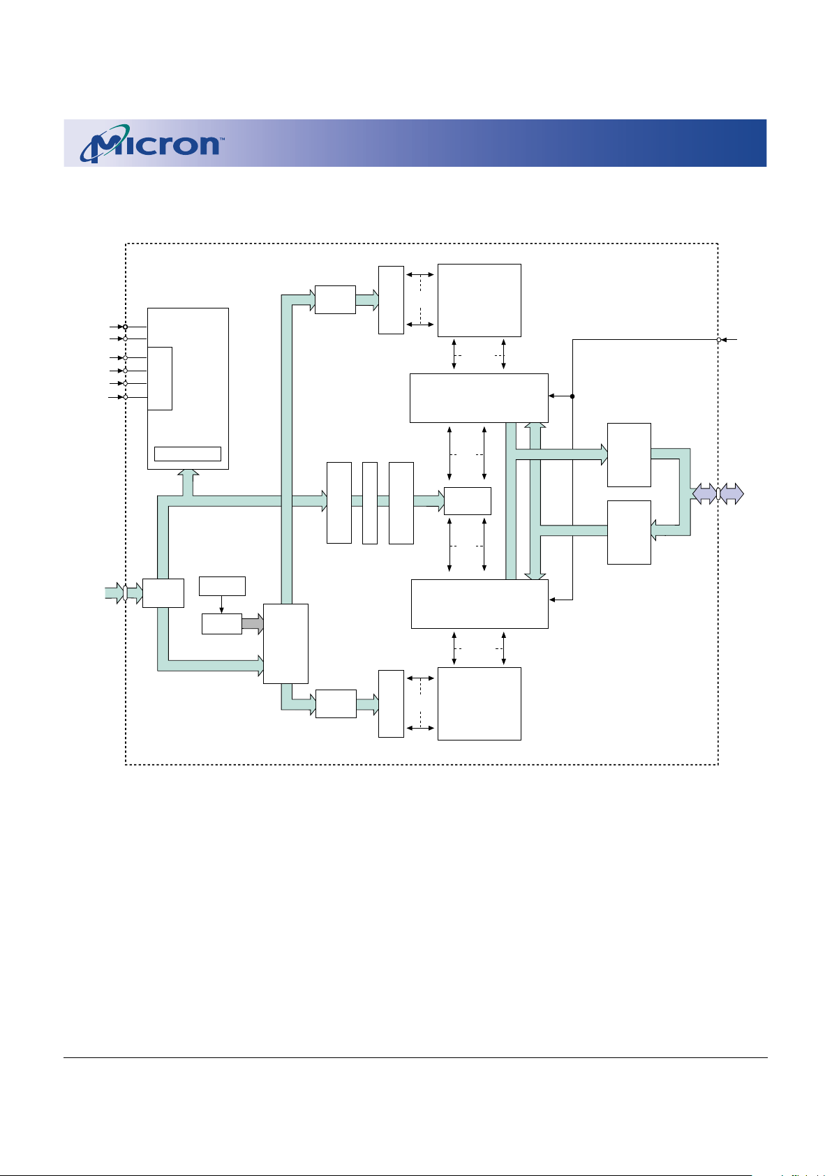
FUNCTIONAL BLOCK DIAGRAM
4 Meg x 4 SDRAM
11
11
11
RAS#
REFRESH
CONTROLLER
2,048
REFRESH
COUNTER
CAS#
1,024
1,024 (x4)
10
COLUMN-
ADDRESS BUFFER
BURST COUNTER
ROW-
ADDRESS
MUX
CLK
CS#
WE#
CKE
1,024 (x4)
BANK 1
MEMORY
ARRAY
(2,048 x 1,024 x 4)
SENSE AMPLIFIERS
I/O GATING
DQM MASK LOGIC
CONTROL
LOGIC
COLUMN
DECODER
COLUMN-
ADDRESS LATCH
10
MODE REGISTER
ROW-
ADDRESS
LATCH
11
ROW
DECODER
11
COMMAND
DECODE
DQ0 -
DQ3
A0-A10, BA
4
8
DQM
1,024
2,048
BANK 0
MEMORY
ARRAY
(2,048 x 1,024 x 4)
ROW
DECODER
ROW-
ADDRESS
LATCH
11
12
ADDRESS
REGISTER
12
SENSE AMPLIFIERS
I/O GATING
DQM MASK LOGIC
DATA
INPUT
REGISTER
DATA
OUTPUT
REGISTER
4
4
5
16 Meg: x4, x8 SDRAM Micron Technology, Inc., reserves the right to change products or specifications without notice.
16MSDRAMx4x8_B.p65 – Rev. 5/98 ©1998, Micron Technology, Inc.
16 MEG: x4, x8
SDRAM
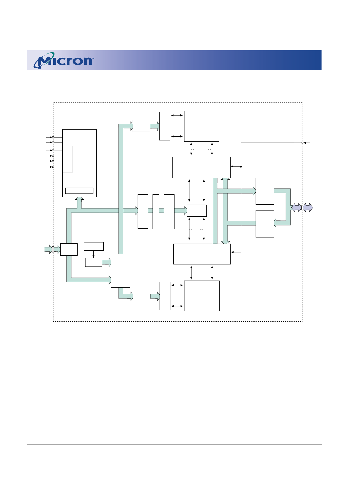
FUNCTIONAL BLOCK DIAGRAM
2 Meg x 8 SDRAM
11
11
11
RAS#
REFRESH
CONTROLLER
2,048
REFRESH
COUNTER
CAS#
512
512 (x8)
9
COLUMN-
ADDRESS BUFFER
BURST COUNTER
ROW-
ADDRESS
MUX
CLK
CS#
WE#
CKE
512 (x8)
BANK 1
MEMORY
ARRAY
(2,048 x 512 x 8)
SENSE AMPLIFIERS
I/O GATING
DQM MASK LOGIC
CONTROL
LOGIC
COLUMN
DECODER
COLUMN-
ADDRESS LATCH
9
MODE REGISTER
ROW-
ADDRESS
LATCH
11
ROW
DECODER
11
COMMAND
DECODE
DQ0 DQ7
A0-A10, BA
8
8
DQM
512
2,048
BANK 0
MEMORY
ARRAY
(2,048 x 512 x 8)
ROW
DECODER
ROW-
ADDRESS
LATCH
11
12
ADDRESS
REGISTER
12
SENSE AMPLIFIERS
I/O GATING
DQM MASK LOGIC
DATA
INPUT
REGISTER
DATA
OUTPUT
REGISTER
8
8
6
16 Meg: x4, x8 SDRAM Micron Technology, Inc., reserves the right to change products or specifications without notice.
16MSDRAMx4x8_B.p65 – Rev. 5/98 ©1998, Micron Technology, Inc.
16 MEG: x4, x8
SDRAM
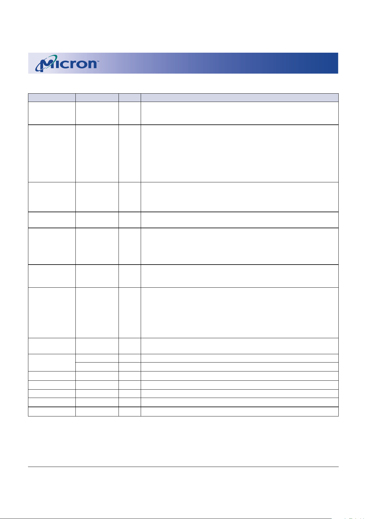
PIN DESCRIPTIONS
PIN NUMBERS SYMBOL TYPE DESCRIPTION
32 CLK Input Clock: CLK is driven by the system clock. All SDRAM input signals are sampled on
the positive edge of CLK. CLK also increments the internal burst counter and
controls the output registers.
31 CKE Input Clock Enable: CKE activates (HIGH) and deactivates (LOW) the CLK signal.
Deactivating the clock provides PRECHARGE POWER-DOWN and SELF REFRESH
operations (all banks idle), ACTIVE POWER-DOWN (row active in either bank), or
CLOCK SUSPEND operation (burst/access in progress). CKE is synchronous except
after the device enters power-down and self refresh modes, where CKE becomes
asynchronous until after exiting the same mode. The input buffers, including
CLK, are disabled during power-down and self refresh modes, providing low
standby power. CKE may be tied HIGH.
15 CS# Input Chip Select: CS# enables (registered LOW) and disables (registered HIGH) the
command decoder. All commands are masked when CS# is registered HIGH. CS#
provides for external bank selection on systems with multiple banks. CS# is
considered part of the command code.
14, 13, RAS#, CAS#, Input Command Inputs: RAS#, CAS#, and WE# (along with CS#) define the command
12 WE# being entered.
33 DQM Input Input/Output Mask: DQM is an input mask signal for write accesses and an
output enable signal for read accesses. Input data is masked when DQM is
sampled HIGH during a WRITE cycle. The output buffers are placed in a High-Z
state (after a two-clock latency) when DQM is sampled HIGH during a READ
cycle.
16 BA Input Bank Address: BA defines to which bank the ACTIVE, READ, WRITE, or
PRECHARGE command is being applied. BA is also used to program the twelfth
bit of the Mode Register.
18-21, 24-29, 17 A0-A10 Input Address Inputs: A0-A10 are sampled during the ACTIVE command (row-address
A0-A10) and READ/WRITE command (column-address A0-A9 [x4]; A0-A8 [x8],
with A9 as a “Don’t Care;” and with A10 defining AUTO PRECHARGE) to select
one location out of the memory array in the respective bank. A10 is sampled
during a PRECHARGE command to determine if both banks are to be
precharged (A10 HIGH). The address inputs also provide the op-code during a
LOAD MODE REGISTER command.
4, 8, 37, 41 x4: DQ0, 1, 2, 3 Input Data I/O: Data bus.
x8: DQ1, 3, 4, 6
2, 6, 39, 43 x4: NC – No Connect: These pins should be left unconnected.
x8: DQ0, 2, 5, 7 Input Data I/O: Data bus.
10, 11, 30, 34, 35 NC – No Connect: These pins should be left unconnected.
5, 9, 36, 40 VDDQ Supply DQ Power.
3, 7, 38, 42 VSSQ Supply DQ Ground.
1, 22 V
DD
Supply Power Supply: +3.3V ±0.3V.
23, 44 V
SS
Supply Ground.

7
16 Meg: x4, x8 SDRAM Micron Technology, Inc., reserves the right to change products or specifications without notice.
16MSDRAMx4x8_B.p65 – Rev. 5/98 ©1998, Micron Technology, Inc.
16 MEG: x4, x8
SDRAM
FUNCTIONAL DESCRIPTION
In general, the SDRAM is a dual memory array (the
4 Meg x 4 is a dual 2 Meg x 4, and the 2 Meg x 8 is a dual
1 Meg x 8) which operates at 3.3V and includes a synchronous interface (all signals are registered on the positive
edge of the clock signal, CLK). Each of the two internal
banks is organized with 2,048 rows and either 1,024 columns by 4 bits (4 Meg x 4) or 512 columns by 8 bits (2 Meg
x 8).
Read and write accesses to the SDRAM are burst oriented; accesses start at a selected location and continue
for a programmed number of locations in a programmed
sequence. Accesses begin with the registration of an ACTIVE command, which is then followed by a READ or
WRITE command. The address bits registered coincident with the ACTIVE command are used to select the
bank and row to be accessed (BA selects the bank, A0-A10
select the row). The address bits (A0-A9; A9 is a “Don’t
Care” for x8) registered coincident with the READ or
WRITE command are used to select the starting column
location for the burst access.
Prior to normal operation, the SDRAM must be initialized. The following sections provide detailed information covering device initialization, register definition,
command descriptions and device operation.
Initialization
SDRAMs must be powered up and initialized in a
predefined manner. Operational procedures other than
those specified may result in undefined operation. Once
power is applied to VDD and VDDQ (simultaneously) and
the clock is stable, the SDRAM requires a 100µs delay
prior to applying an executable command. The RAS#,
CAS#, WE# and CS# inputs should be held HIGH during
this phase of power-up.
Once the 100µs delay has been satisfied, CKE HIGH
and the PRECHARGE command can be applied (set up
and held with respect to a positive edge of CLK). Both
banks must then be precharged, thereby placing the
device in the all banks idle state.
Once in the idle state, two AUTO REFRESH cycles
must be performed. After the AUTO REFRESH cycles are
complete, the SDRAM is ready for Mode Register programming. Because the Mode Register will power up in
an unknown state, it should be loaded prior to applying
any operational command.
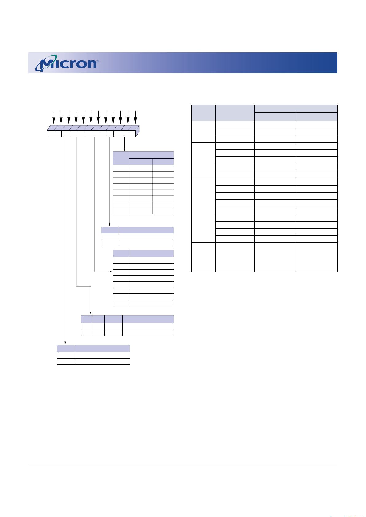
Register Definition
MODE REGISTER
The Mode Register is used to define the specific mode
of operation of the SDRAM. This definition includes the
selection of a burst length, a burst type, a CAS latency, an
operating mode, and a write burst mode, as shown in
Figure 1. The Mode Register is programmed via the LOAD
MODE REGISTER command and will retain the stored
information until it is programmed again or the device
loses power.
Mode Register bits M0-M2 specify the burst length,
M3 specifies the type of burst (sequential or interleaved),
M4-M6 specify the CAS latency, M7 and M8 specify the
operating mode, M9 specifies the write burst mode, and
M10 and M11 are reserved for future use.
The Mode Register must be loaded when both banks
are idle, and the controller must wait the specified time
before initiating the subsequent operation. Violating either of these requirements will result in unspecified operation.
Burst Length
Read and write accesses to the SDRAM are burst oriented, with the burst length being programmable, as
shown in Figure 1. The burst length determines the maximum number of column locations that can be accessed
for a given READ or WRITE command. Burst lengths of 1,
2, 4 or 8 locations are available for both the sequential
and the interleaved burst types, and a full-page burst is
available for the sequential type. The full-page burst is
used in conjunction with the BURST TERMINATE command to generate arbitrary burst lengths.
Reserved states should not be used, as unknown operation or incompatibility with future versions may result.
When a READ or WRITE command is issued, a block
of columns equal to the burst length is effectively selected. All accesses for that burst take place within this
block, meaning that the burst will wrap within the block
if a boundary is reached. The block is uniquely selected
by A1-A9 (A9 is “Don’t Care” for x8) when the burst length
is set to two; by A2-A9 (A9 is “Don’t Care” for x8) when the
burst length is set to four; and by A3-A9 (A9 is “Don’t
Care” for x8) when the burst length is set to eight. The
remaining (least significant) address bit(s) is (are) used to
select the starting location within the block. Full-page
bursts wrap within the page if the boundary is reached.
Burst Type
Accesses within a given burst may be programmed to
be either sequential or interleaved; this is referred to as
the burst type and is selected via bit M3.
The ordering of accesses within a burst is determined
by the burst length, the burst type and the starting column address, as shown in Table 1.
8
16 Meg: x4, x8 SDRAM Micron Technology, Inc., reserves the right to change products or specifications without notice.
16MSDRAMx4x8_B.p65 – Rev. 5/98 ©1998, Micron Technology, Inc.
16 MEG: x4, x8
SDRAM
NOTE: 1. For a burst length of two, A1-A9 select the block
of two burst (A9 is a “Don’t Care” for x8); A0
selects the starting column within the block.
2. For a burst length of four, A2-A9 select the block
of four burst (A9 is a “Don’t Care” for x8); A0-A1
select the starting column within the block.
3. For a burst length of eight, A3-A9 select the block
of eight burst (A9 is a “Don’t Care” for x8); A0-A2
select the starting column within the block.
4. For a full-page burst, the full row is selected and
A0-A9 select the starting column (A9 is a “Don’t
Care” for x8).
5. Whenever a boundary of the block is reached
within a given sequence above, the following
access wraps within the block.
6. For a burst length of one, A0-A9 select the unique
column to be accessed (A9 is a “Don’t Care” for
x8), and Mode Register bit M3 is ignored.
Table 1
Burst Definition
Burst Starting Column Order of Accesses Within a Burst
Length Address: Type = Sequential Type = Interleaved
A0
2
0 0-1 0-1
1 1-0 1-0
A1 A0
0 0 0-1-2-3 0-1-2-3
4
0 1 1-2-3-0 1-0-3-2
1 0 2-3-0-1 2-3-0-1
1 1 3-0-1-2 3-2-1-0
A2 A1 A0
0 0 0 0-1-2-3-4-5-6-7 0-1-2-3-4-5-6-7
0 0 1 1-2-3-4-5-6-7-0 1-0-3-2-5-4-7-6
0 1 0 2-3-4-5-6-7-0-1 2-3-0-1-6-7-4-5
8
0 1 1 3-4-5-6-7-0-1-2 3-2-1-0-7-6-5-4
1 0 0 4-5-6-7-0-1-2-3 4-5-6-7-0-1-2-3
1 0 1 5-6-7-0-1-2-3-4 5-4-7-6-1-0-3-2
1 1 0 6-7-0-1-2-3-4-5 6-7-4-5-2-3-0-1
1 1 1 7-0-1-2-3-4-5-6 7-6-5-4-3-2-1-0
Full x4: n = A0-A9
Cn, Cn+1, Cn+2
Page x8: n = A0-A8
Cn+3, Cn+4...
Not supported
(x4: 1,024) (location 0-1,023)
…Cn-1,
(x8: 512) (location 0-511) Cn…
M2
0
0
0
0
1
1
1
1
M1
0
0
1
1
0
0
1
1
M0
0
1
0
1
0
1
0
1
M3 = 0
1
2
4
8
Reserved
Reserved
Reserved
Full Page
M3 = 1
1
2
4
8
Reserved
Reserved
Reserved
Reserved
Operating Mode
Standard Operation
All other states reserved
0-0-Defined
-
0
1
Burst Type
Sequential
Interleaved
CAS Latency
Reserved
1
2
3
Reserved
Reserved
Reserved
Reserved
M6
0
0
0
0
1
1
1
1
M4
0
1
0
1
0
1
0
1
M5
0
0
1
1
0
0
1
1
Burst Length
Burst LengthCAS Latency B T
A9
A7
A6 A5 A4
A3A8A2A1A0
Mode Register (Mx)
Address Bus
9
7
654
382
1
0
M3
M6-M0
M8
M7
Op Mode
A10
BA
10
11
Reserved* WB
0
1
Write Burst Mode
Programmed Burst Length
Single Location Access
M9
*Should program
M11, M10 = 0, 0
to ensure compatibility
with future devices.
Figure 1
Mode Register Definition
9
16 Meg: x4, x8 SDRAM Micron Technology, Inc., reserves the right to change products or specifications without notice.
16MSDRAMx4x8_B.p65 – Rev. 5/98 ©1998, Micron Technology, Inc.
16 MEG: x4, x8
SDRAM
ALLOWABLE OPERATING
FREQUENCY (MHz)
CAS CAS CAS
SPEED LATENCY = 1 LATENCY = 2 LATENCY = 3
-8D/E £ 33 £ 100 £ 125
-8A/B/C £ 33 £ 83 £ 125
-10 £ 33 £ 66 £ 100
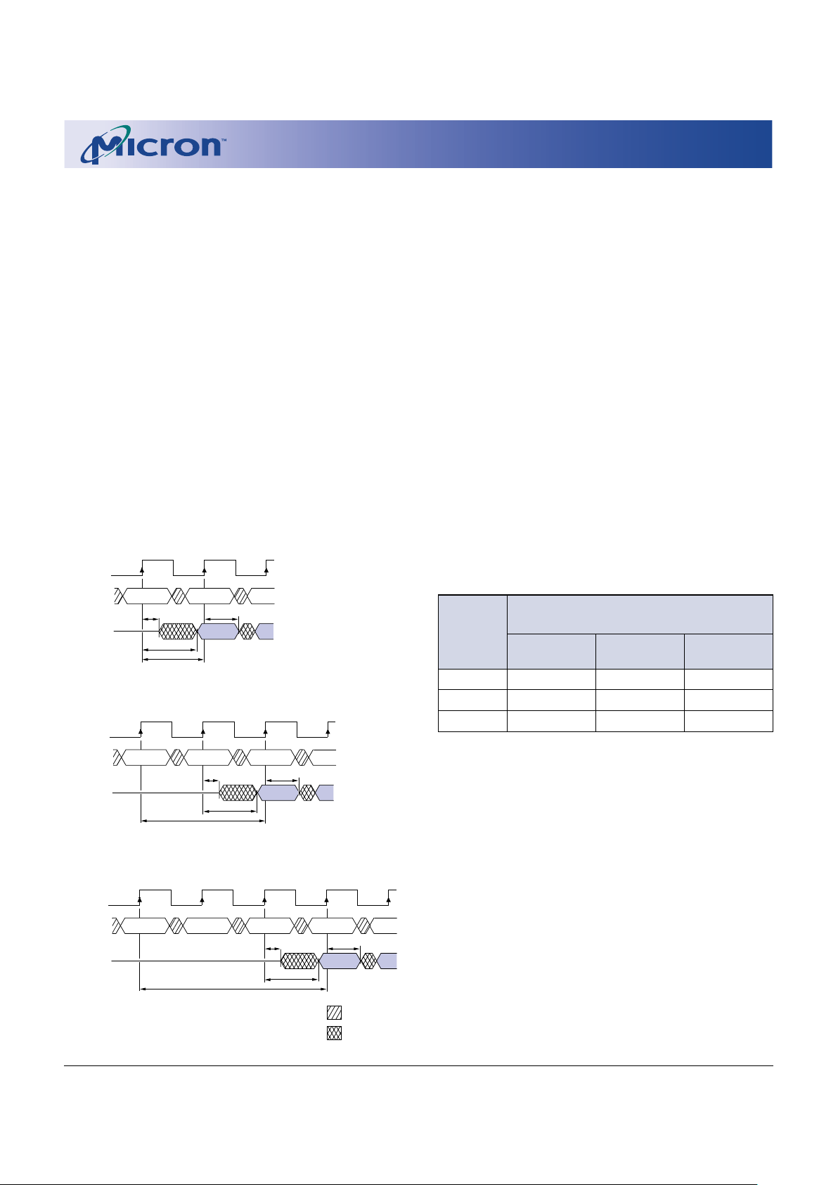
CAS Latency
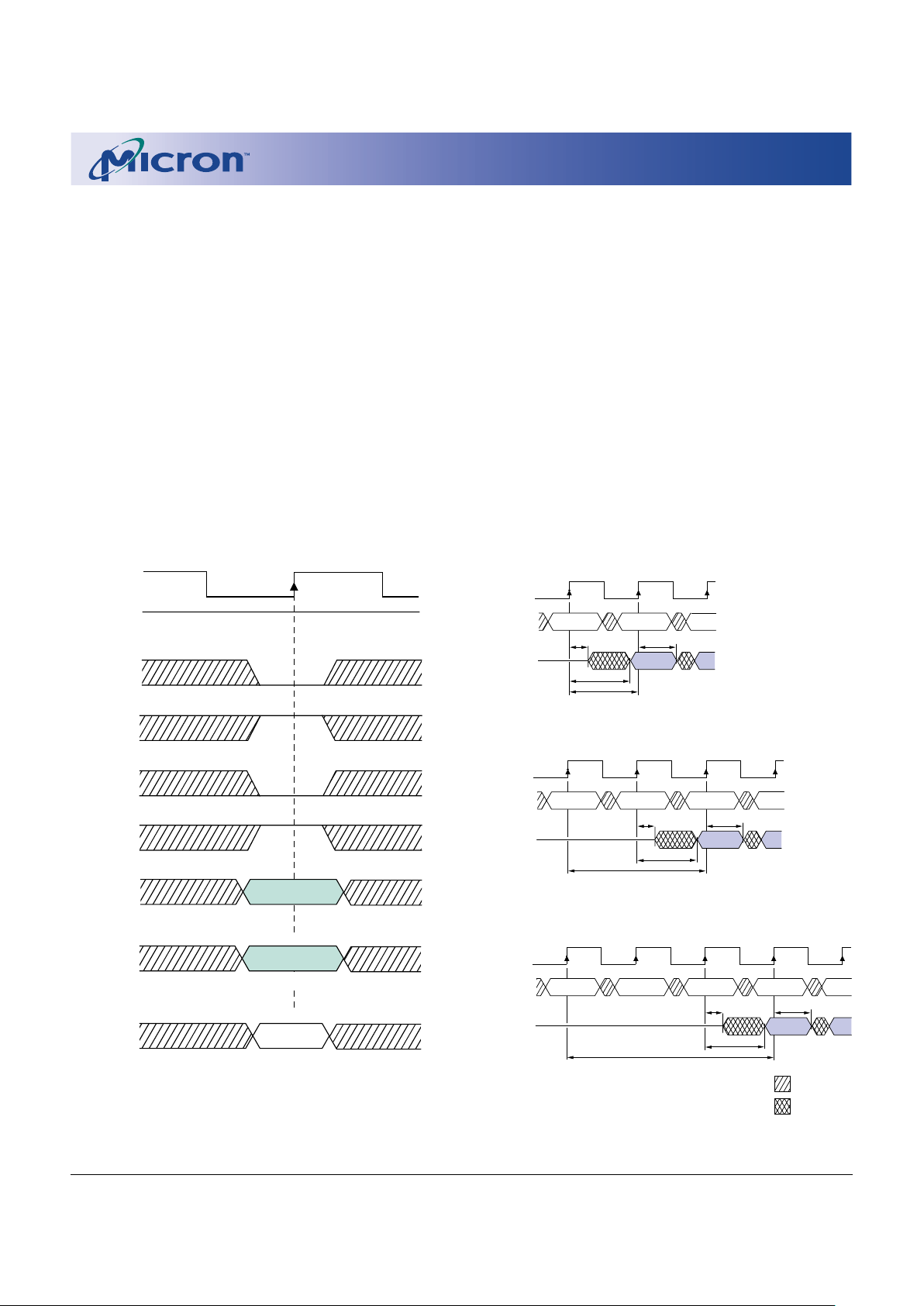
The CAS latency is the delay, in clock cycles, between
the registration of a READ command and the availability
of the first piece of output data. The latency can be set to
1, 2, or 3 clocks.
If a READ command is registered at clock edge n, and
the latency is m clocks, the data will be available by clock
edge n + m. The DQs will start driving as a result of the
clock edge one cycle earlier (n + m - 1) and, provided that
the relevant access times are met, the data will be valid by
clock edge n + m. For example, assuming that the clock
cycle time is such that all relevant access times are met,
if a READ command is registered at T0, and the latency is
programmed to two clocks, the DQs will start driving
after T1 and the data will be valid by T2, as shown in
Figure 2. Table 2 below indicates the operating frequencies at which each CAS latency setting can be used.
Reserved states should not be used, as unknown operation or incompatibility with future versions may result.
Operating Mode
The normal operating mode is selected by setting M7
and M8 to zero; the other combinations of values for M7
and M8 are reserved for future use and/or test modes.
The programmed burst length applies to both READ and
WRITE bursts.
Test modes and reserved states should not be used
because unknown operation or incompatibility with future versions may result.
Write Burst Mode
When M9 = 0, the burst length programmed via M0M2 applies to both READ and WRITE bursts; when
M9 = 1, the programmed burst length applies to READ
bursts, but write accesses are single-location (nonburst)
accesses.
CLK
DQ
T2T1 T3T0
CAS Latency = 3
LZ
D
OUT
t
OH
t
COMMAND
NOPREAD
t
AC
NOP
T4
NOP
DON’T CARE
UNDEFINED
CLK
DQ
T2T1T0
CAS Latency = 1
LZ
D
OUT
t
OH
t
COMMAND
NOPREAD
t
AC
CLK
DQ
T2T1 T3T0
CAS Latency = 2
LZ
D
OUT
t
OH
t
COMMAND
NOPREAD
t
AC
NOP
Figure 2
CAS LATENCY
Table 2
CAS LATENCY
10
16 Meg: x4, x8 SDRAM Micron Technology, Inc., reserves the right to change products or specifications without notice.
16MSDRAMx4x8_B.p65 – Rev. 5/98 ©1998, Micron Technology, Inc.
16 MEG: x4, x8
SDRAM
TRUTH TABLE 1 – Commands and DQM Operation
(Note: 1)
NAME (FUNCTION) CS# RAS# CAS# WE# DQM ADDR DQs NOTES
COMMAND INHIBIT (NOP) H XXXX X X
NO OPERATION (NOP) L H H H X X X
ACTIVE (Select bank and activate row) L L H H X Bank/Row X 3
READ (Select bank and column and start READ burst) L H L H X Bank/Col X 4
WRITE (Select bank and column and L H L L X Bank/Col Valid 4
start WRITE burst)
BURST TERMINATE L H H L X X Active
PRECHARGE (Deactivate row in bank or banks) L L H L X Code X 5
AUTO REFRESH or L L L H X X X 6, 7
SELF REFRESH (Enter self refresh mode)
LOAD MODE REGISTER L L L L X Op-code X 2
Write Enable/Output Enable ––––L – Active 8
Write Inhibit/Output High-Z ––––H –High-Z 8
following the Operation section; these tables provide
current state/next state information.
COMMANDS
Truth Table 1 provides a quick reference of available commands. This is followed by a written description
of each command. Two additional Truth Tables appear
NOTE: 1. CKE is HIGH for all commands shown except SELF REFRESH.
2. A0-A10 and BA define the op-code written to the Mode Register.
3. A0-A10 provide row address, and BA determines which bank is made active (BA LOW = Bank 0; BA HIGH = Bank 1).
4. A0-A9 (A9 is a “Don’t Care” for x8) provide column address; A10 HIGH enables the auto precharge feature (nonpersistent), while A10 LOW disables the auto precharge feature; BA determines which bank is being read from or written to
(BA LOW = Bank 0; BA HIGH = Bank 1).
5. For A10 LOW, BA determines which bank is being precharged (BA LOW = Bank 0; BA HIGH = Bank 1); for A10 HIGH,
both banks are precharged and BA is a “Don’t Care.”
6. This command is AUTO REFRESH if CKE is HIGH, SELF REFRESH if CKE is LOW.
7. Internal refresh counter controls row addressing; all inputs and I/Os are “Don’t Care” except for CKE.
8. Activates or deactivates the DQs during WRITEs (zero-clock delay) and READs (two-clock delay).

11
16 Meg: x4, x8 SDRAM Micron Technology, Inc., reserves the right to change products or specifications without notice.
16MSDRAMx4x8_B.p65 – Rev. 5/98 ©1998, Micron Technology, Inc.
16 MEG: x4, x8
SDRAM
COMMAND INHIBIT
The COMMAND INHIBIT function prevents new commands from being executed by the SDRAM, regardless of
whether the CLK signal is enabled. The SDRAM is effectively deactivated, or deselected.
NO OPERATION (NOP)
The NO OPERATION (NOP) command is used to perform a NOP to an SDRAM which is selected (CS# is LOW).
This prevents unwanted commands from being registered during idle or wait states.
LOAD MODE REGISTER
The Mode Register is loaded via inputs A0-A10 and
BA. See Mode Register heading in Register Definition
section. The LOAD MODE REGISTER command can only
be issued when both banks are idle, and a subsequent
executable command cannot be issued until tMRD is
met.
ACTIVE
The ACTIVE command is used to open (or activate) a
row in a particular bank for a subsequent access. The
value on the BA input selects the bank, and the address
provided on inputs A0-A10 selects the row. This row
remains active (or open) for accesses until a PRECHARGE
command is issued to that bank. A PRECHARGE command must be issued before opening a different row in
the same bank.
READ
The READ command is used to initiate a burst read
access to an active row. The value on the BA input selects
the bank, and the address provided on inputs A0-A9 (A9
is a “Don’t Care” on x8) selects the starting column
location. The value on input A10 determines whether or
not auto precharge is used. If auto precharge is selected,
the row being accessed will be precharged at the end of
the READ burst; if auto precharge is not selected, the row
will remain open for subsequent accesses. Read data
appears on the DQs, subject to the logic level on the DQM
input, two clocks earlier. If the DQM signal was registered HIGH, the DQs will be High-Z two clocks later; if the
DQM signal was registered LOW, the DQs will provide
valid data.
WRITE
The WRITE command is used to initiate a burst write
access to an active row. The value on the BA input selects
the bank, and the address provided on inputs A0-A9 (A9
is a “Don’t Care” on x8) selects the starting column
location. The value on input A10 determines whether or
not auto precharge is used. If auto precharge is selected,
the row being accessed will be precharged at the end of
the WRITE burst; if auto precharge is not selected, the
row will remain open for subsequent accesses. Input
data appearing on the DQs is written to the memory array
subject to the DQM input logic level appearing coincident with the data. If the DQM signal is registered LOW,
the corresponding data will be written to memory; if the
DQM signal is registered HIGH, the corresponding data
inputs will be ignored, and a WRITE will not be executed
to that location.
PRECHARGE
The PRECHARGE command is used to deactivate the
open row in a particular bank or the open row in both
banks. The bank(s) will be available for a subsequent row
access some specified time (tRP) after the PRECHARGE
command is issued. Input A10 determines whether one
or both banks are to be precharged, and in the case where
only one bank is to be precharged, input BA selects the
bank. Otherwise BA is treated as a “Don’t Care.” Once a
bank has been precharged, it is in the idle state and must
be activated prior to any READ or WRITE commands
being issued to that bank.
AUTO PRECHARGE
Auto precharge is a feature which performs the same
individual-bank PRECHARGE function described above,
without requiring an explicit command. This is accomplished by using A10 to enable auto precharge in conjunction with a specific READ or WRITE command. A
PRECHARGE of the bank/row that is addressed with the
READ or WRITE command is automatically performed
upon completion of the READ or WRITE burst, except in
the full-page burst mode, where auto precharge does not
apply. Auto precharge is nonpersistent in that it is either
enabled or disabled for each individual READ or WRITE
command.
Auto precharge ensures that the PRECHARGE is initiated at the earliest valid stage within a burst. The user
must not issue another command until the precharge
time (tRP) is completed. This is determined as if an explicit PRECHARGE command was issued at the earliest
possible time, as described for each burst type in the
Operation section of this data sheet.
BURST TERMINATE
The BURST TERMINATE command is used to truncate either fixed-length or full-page bursts. The most
recently registered READ or WRITE command prior to
the BURST TERMINATE command will be truncated, as
shown in the Operation section of this data sheet.

12
16 Meg: x4, x8 SDRAM Micron Technology, Inc., reserves the right to change products or specifications without notice.
16MSDRAMx4x8_B.p65 – Rev. 5/98 ©1998, Micron Technology, Inc.
16 MEG: x4, x8
SDRAM
AUTO REFRESH
AUTO REFRESH is used during normal operation of
the SDRAM and is analagous to CAS#-BEFORE-RAS#
(CBR) REFRESH in conventional DRAMs. This command
is nonpersistent, so it must be issued each time a refresh
is required.
The addressing is generated by the internal refresh
controller. This makes the address bits “Don’t Care”
during an AUTO REFRESH command. The Micron 16Mb
SDRAM requires all of its 4,096 rows to be refreshed every
64ms (tREF). Providing a distributed AUTO REFRESH
command every 15.6µs will meet the refresh requirement and ensure that each row is refreshed. Alternatively, all 4,096 AUTO REFRESH commands can be issued in a burst at the minimum cycle rate (tRC) once
every 64ms.
SELF REFRESH
The SELF REFRESH command can be used to retain data in the SDRAM, even if the rest of the system is
powered down. When in the self refresh mode, the SDRAM
retains data without external clocking. The SELF RE-
FRESH command is initiated like an AUTO REFRESH
command except CKE is disabled (LOW). Once the SELF
REFRESH command is registered, all the inputs to the
SDRAM become “Don’t Care,” with the exception of
CKE, which must remain LOW.
Once self refresh mode is engaged, the SDRAM provides its own internal clocking, causing it to perform its
own AUTO REFRESH cycles. The SDRAM must remain in
self refresh mode for a minimum period equal to tRAS
and may remain in self refresh mode for an indefinite
period beyond that.
The procedure for exiting self refresh requires a sequence of commands. First, CLK must be stable prior to
CKE going back HIGH. Once CKE is HIGH, the SDRAM
must have NOP commands issued (a minimum of two
clocks) for tXSR because time is required for the completion of any internal refresh in progress.
A burst of 4,096 AUTO REFRESH cycles should be
completed just prior to entering and just after exiting the
self refresh mode.
13
16 Meg: x4, x8 SDRAM Micron Technology, Inc., reserves the right to change products or specifications without notice.
16MSDRAMx4x8_B.p65 – Rev. 5/98 ©1998, Micron Technology, Inc.
16 MEG: x4, x8
SDRAM
OPERATION
BANK/ROW ACTIVATION
Before any READ or WRITE commands can be issued
to a bank within the SDRAM, a row in that bank must be
“opened.” This is accomplished via the ACTIVE command, which selects both the bank and the row to be
activated.
After opening a row (issuing an ACTIVE command), a
READ or WRITE command may be issued to that row,
subject to the tRCD specification. tRCD (MIN) should be
divided by the clock period and rounded up to the next
whole number to determine the earliest clock edge after
the ACTIVE command on which a READ or WRITE command can be entered. For example, a tRCD specification
of 30ns with a 90 MHz clock (11.11ns period) results in 2.7
clocks, rounded to 3. This is reflected in Figure 4, which
covers any case where 2 < tRCD (MIN)/tCK < 3. (The same
procedure is used to convert other specification limits
from time units to clock cycles.)
A subsequent ACTIVE command to a different row in
the same bank can only be issued after the previous
active row has been “closed” (precharged). The minimum time interval between successive ACTIVE commands to the same bank is defined by tRC.
A subsequent ACTIVE command to the other bank
can be issued while the first bank is being accessed,
resulting in a reduction of total row access overhead. The
minimum time interval between successive ACTIVE commands to different banks is defined by tRRD.
CS#
WE#
CAS#
RAS#
CKE
CLK
A0-A10
BA
ROW
ADDRESS
HIGH
BANK 0
BANK 1
Figure 3
Activating a Specific Row in a
Specific Bank
CLK
T2T1 T3T0
t
COMMAND
NOPACTIVE
READ or
WRITE
T4
NOP
RCD
DON’T CARE
Figure 4
EXAMPLE: MEETING tRCD (MIN) WHEN 2 < tRCD (MIN)/tCK < 3
14
16 Meg: x4, x8 SDRAM Micron Technology, Inc., reserves the right to change products or specifications without notice.
16MSDRAMx4x8_B.p65 – Rev. 5/98 ©1998, Micron Technology, Inc.
16 MEG: x4, x8
SDRAM
Upon completion of a burst, assuming no other commands have been initiated, the DQs will go High-Z. A fullpage burst will continue until terminated. (At the end of
the page, it will wrap to column 0 and continue.)
A fixed-length READ burst may be followed by, or
truncated with, a READ burst (provided that auto
precharge is not activated), and a full-page READ burst
can be truncated with a subsequent READ burst. In either
case, a continuous flow of data can be maintained. The
first data element from the new burst follows either the
last element of a completed burst or the last desired data
element of a longer burst that is being truncated. The
new READ command should be issued x cycles before
the clock edge at which the last desired data element is
valid, where x equals the CAS latency minus one. This is
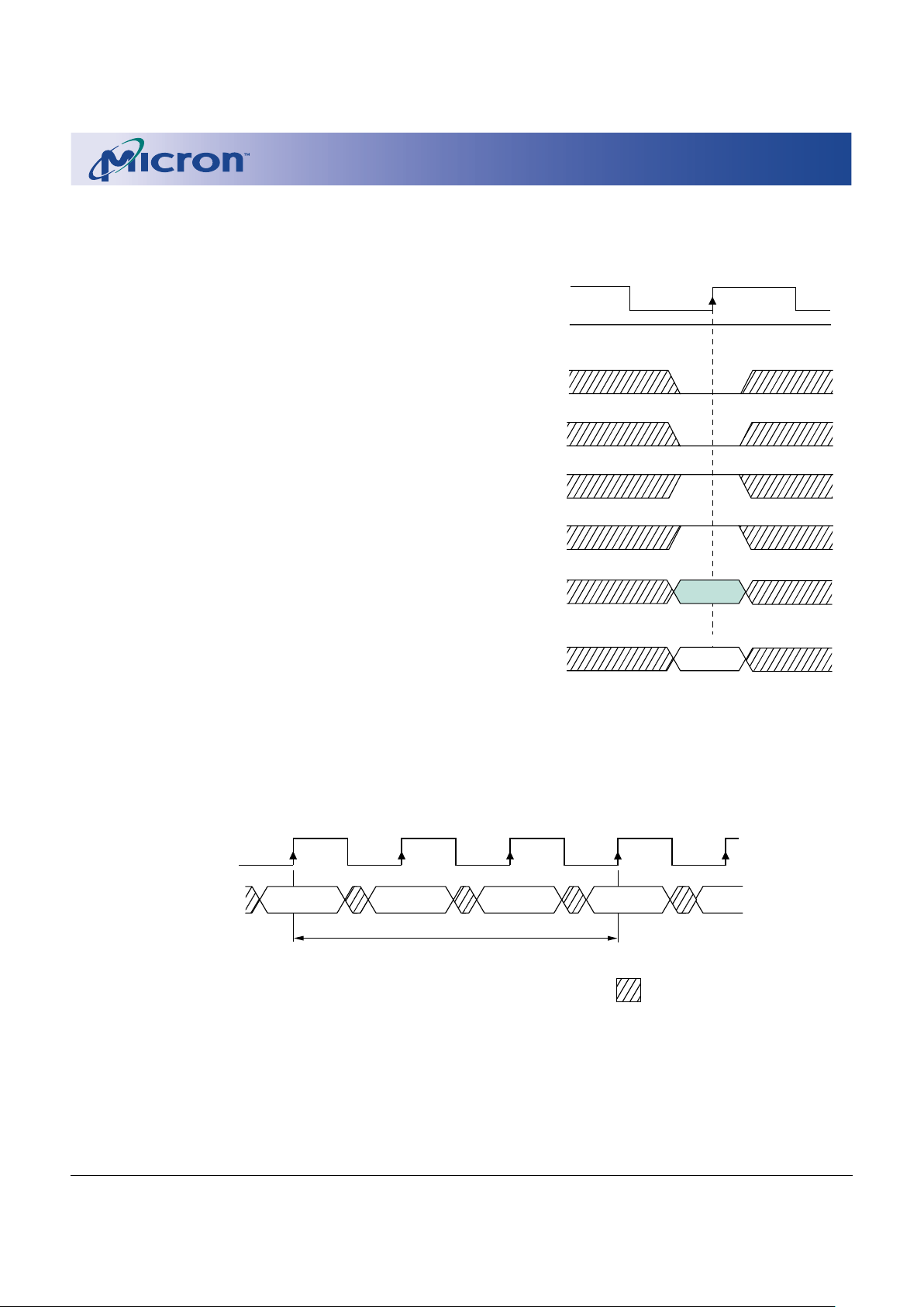
READs
READ bursts are initiated with a READ command, as
shown in Figure 5 (A9 is a “Don’t Care”on x8).
The starting column and bank addresses are provided with the READ command, and auto precharge is
either enabled or disabled for that burst access. If auto
precharge is enabled, the row being accessed is
precharged at the completion of the burst. For the generic READ commands used in the following illustrations, auto precharge is disabled.
During READ bursts, the valid data-out element from
the starting column address will be available following
the CAS latency after the READ command. Each subsequent data-out element will be valid by the next positive
clock edge. Figure 6 shows general timing for each possible CAS latency setting.
CS#
WE#
CAS#
RAS#
CKE
CLK
COLUMN
ADDRESS
A0-A9
A10
BA
BANK 0
BANK 1
HIGH
ENABLE AUTO PRECHARGE
DISABLE AUTO PRECHARGE
(
A9 is a “Don’t Care” for x8)
Figure 5
READ Command
CLK
DQ
T2T1 T3T0
CAS Latency = 3
LZ
D
OUT
t
OH
t
COMMAND
NOPREAD
t
AC
NOP
T4
NOP
DON’T CARE
UNDEFINED
CLK
DQ
T2T1T0
CAS Latency = 1
LZ
D
OUT
t
OH
t
COMMAND
NOPREAD
t
AC
CLK
DQ
T2T1 T3T0
CAS Latency = 2
LZ
D
OUT
t
OH
t
COMMAND
NOPREAD
t
AC
NOP
Figure 6
CAS Latency
15
16 Meg: x4, x8 SDRAM Micron Technology, Inc., reserves the right to change products or specifications without notice.
16MSDRAMx4x8_B.p65 – Rev. 5/98 ©1998, Micron Technology, Inc.
16 MEG: x4, x8
SDRAM
shown in Figure 7 for CAS latencies of one, two and three;
data element n + 3 is either the last of a burst of four or the
last desired of a longer burst. The Micron 16Mb SDRAM
uses a pipelined architecture and therefore does not
require the 2n rule associated with a prefetch architec-
Figure 7
Consecutive READ Bursts
ture. A READ command can be initiated on any clock
cycle following a previous READ command. Full-speed
random read accesses can be performed to the same
bank, as shown in Figure 8, or each subsequent READ
may be performed to a different bank.
CLK
DQ
D
OUT
n
T2T1 T4T3 T5T0
COMMAND
ADDRESS
READ NOP NOP NOP
BANK,
COL n
DON’T CARE
NOP
BANK,
COL b
D
OUT
n + 1
D
OUT
n + 2
D
OUT
n + 3
D
OUT
b
READ
X = 0 cycles
NOTE: Each READ command may be to either bank. DQM is LOW.
CAS Latency = 1
CLK
DQ
D
OUT
n
T2T1 T4T3 T6T5T0
COMMAND
ADDRESS
READ NOP NOP NOP NOP
BANK,
COL n
NOP
BANK,
COL b
D
OUT
n + 1
D
OUT
n + 2
D
OUT
n + 3
D
OUT
b
READ
X = 1 cycle
CAS Latency = 2
CLK
DQ
D
OUT
n
T2T1 T4T3 T6T5T0
COMMAND
ADDRESS
READ NOP NOP NOP NOP
BANK,
COL n
NOP
BANK,
COL b
D
OUT
n + 1
D
OUT
n + 2
D
OUT
n + 3
D
OUT
b
READ
NOP
T7
X = 2 cycles
CAS Latency = 3
 Loading...