

MICRON MT46V32M4TG-75Z, MT46V16M8TG-75, MT46V8M16TG-8 Datasheet
PRELIMINARY
128Mb: x4, x8, x16
DDR SDRAM
‡
DOUBLE DATA RATE
(DDR) SDRAM
FEATURES
•VDD = +2.5V ±0.2V, VDDQ = +2.5V ±0.2V
• Bidirectional data strobe (DQS) transmitted/
received with data, i.e., source-synchronous data
capture (x16 has two – one per byte)
• Internal, pipelined double-data-rate (DDR)
architecture; two data accesses per clock cycle
• Differential clock inputs (CK and CK#)
• Commands entered on each positive CK edge
• DQS edge-aligned with data for READs; centeraligned with data for WRITEs
• DLL to align DQ and DQS transitions with CK
• Four internal banks for concurrent operation
• Data mask (DM) for masking write data (x16 has
two – one per byte)
• x16 has programmable IOL/IOH option
• Programmable burst lengths: 2, 4, or 8
• Auto precharge option
• Auto Refresh and Self Refresh Modes
• Longer lead TSOP for improved reliability (OCPL)
• 2.5V I/O (SSTL_2 compatible)
OPTIONS MARKING
• Configuration
32 Meg x 4 (8 Meg x 4 x 4 banks) 32M4
16 Meg x 8 (4 Meg x 8 x 4 banks) 16M8
8 Meg x 16 (2 Meg x 16 x 4 banks) 8M16
MT46V32M4 – 8 Meg x 4 x 4 banks
MT46V16M8 – 4 Meg x 8 x 4 banks
MT46V8M16 – 2 Meg x 16 x 4 banks
For the latest data sheet revisions, please refer to the Micron
Web site: www.micron.com/datasheets
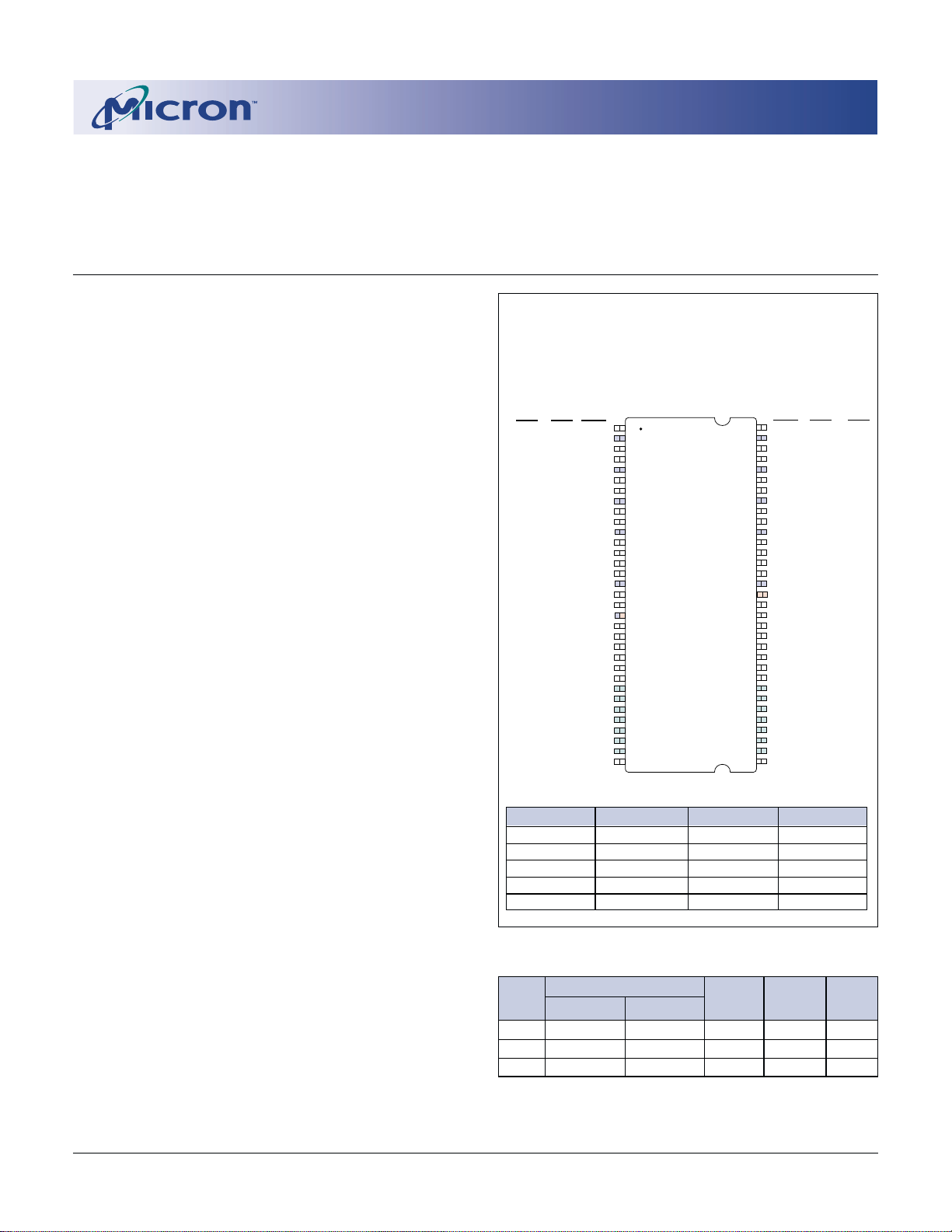
PIN ASSIGNMENT (TOP VIEW)
66-Pin TSOP
V
V
DD
DQ0
V
SS
V
DD
DQ1
V
SS
V
DD
V
WE#
CAS#
RAS#
CS#
BA0
BA1
A10/AP
V
NC
NC
NC
NC
NC
NC
NC
NC
NC
NC
NC
NC
A0
A1
A2
A3
DD
Q
Q
Q
Q
Q
DD
DD
x8x4
V
DQ0
V
DD
DQ1
V
SS
DQ2
V
DD
DQ3
V
SS
V
DD
V
DNU
WE#
CAS#
RAS#
CS#
BA0
BA1
A10/AP
V
DD
NC
NC
NC
NC
NC
NC
NC
DD
NC
NC
A0
A1
A2
A3
DD
Q
Q
Q
Q
Q
x16
V
DQ0
VDDQ
DQ1
DQ2
VssQ
DQ3
DQ4
VDDQ
DQ5
DQ6
VssQ
DQ7
V
DD
LDQS
V
DNU
LDM
WE#
CAS#
RAS#
CS#
BA0
BA1
A10/AP
V
1
DD
2
3
4
5
6
7
8
9
10
11
12
13
14
NC
15
Q
16
17
NC
18
DD
19
20
21
22
23
24
25
NC
26
27
28
29
A0
30
A1
31
A2
32
A3
33
DD
66
65
64
63
62
61
60
59
58
57
56
55
54
53
52
51
50
49
48
47
46
45
44
43
42
41
40
39
38
37
36
35
34
x16
V
SS
DQ15
V
SS
DQ14
DQ13
V
DD
DQ12
DQ11
V
SS
DQ10
DQ9
V
DD
DQ8
NC
V
SS
UDQS
DNU
V
REF
V
SS
UDM
CK#
CK
CKE
NC
NC
A11
A9
A8
A7
A6
A5
A4
V
SS
Q
Q
Q
Q
Q
x8 x4
V
SS
DQ7
V
SS
Q
NC
DQ6
V
DD
Q
NC
DQ5
V
SS
Q
NC
DQ4
V
DD
Q
NC
NC
V
SS
Q
DQS
DNU
V
REF
V
SS
DM
CK#
CK
CKE
NC
NC
A11
A9
A8
A7
A6
A5
A4
V
SS
SS
V
NC
V
SS
NC
DQ3
V
DD
NC
NC
V
SS
NC
DQ2
V
DD
NC
NC
V
SS
DQS
DNU
V
REF
V
SS
DM
CK#
CK
CKE
NC
NC
A11
A9
A8
A7
A6
A5
A4
V
SS
Q
Q
Q
Q
Q
• Plastic Package – OCPL
66-pin TSOP TG
(400 mil width, 0.65mm pin pitch)
• Timing – Cycle Time
7.5ns @ CL = 2 (DDR266B)
7.5ns @ CL = 2.5 (DDR266B)
10ns @ CL = 2 (DDR200)
1
2
3
-75Z
-75
-8
Configuration 8 Meg x 4 x 4 banks 4 Meg x 8 x 4 banks 2 Meg x 16 x 4 banks
Refresh Count 4K 4K 4K
Row Addressing 4K (A0–A11) 4K (A0–A11) 4K (A0–A11)
Bank Addressing 4 (BA0, BA1) 4 (BA0, BA1) 4 (BA0, BA1)
Column Addressing 2K (A0–A9, A11) 1K (A0–A9) 512 (A0–A8)
32 Meg x 4 16 Meg x 8 8 Meg x 16
• Self Refresh
Standard none
KEY TIMING PARAMETERS
Low Power L
SPEE D CLOCK RATE DATA-OUT ACCESS DQS-DQ
NOTE: 1. Supports PC2100 modules with 2-3-3 timing
2. Supports PC2100 modules with 2.5-3-3 timing
3. Supports PC1600 modules with 2-2-2 timing
128Mb: x4, x8, x16 DDR SDRAM Micron Technology, Inc., reserves the right to change products or specifications without notice.
128Mx4x8x16DDR_C.p65 – Rev. C; Pub. 4/01 ©2001, Micron Technology, Inc.
‡ PRODUCTS AND SPECIFICATIONS DISCUSSED HEREIN ARE FOR EVALUATION AND REFERENCE PURPOSES ONLY AND ARE
SUBJECT TO CHANGE BY MICRON WITHOUT NOTICE. PRODUCTS ARE ONLY WARRANTED BY MICRON TO MEET MICRON’S
PRODUCTION DATA SHEET SPECIFICATIONS.
GRADE CL = 2** CL = 2.5** WINDOW* WINDOW SKEW
-75Z 133 MHz 133 MHz 2.5ns ±0.75ns +0.5ns
-75 100 MHz 133 MHz 2.5ns ±0.75ns +0.5ns
-8 100 MHz 125 MHz 3.4ns ±0.8ns +0.6ns
*Minimum clock rate @ CL = 2 (-75Z and -8) and CL = 2.5 (-75)
**CL = CAS (Read) Latency
1

PRELIMINARY
128Mb: x4, x8, x16
DDR SDRAM
128MB DDR SDRAM PART NUMBERS
(Note: xx= -75, -75Z, or -8)
PART NUMBER CONFIGURATION I/O DRIVE LEVEL REFRESH OPTION
MT46V32M4TG-xx 32 Meg x 4 Full Drive Standard
MT46V32M4TG-xxL 32 Meg x 4 Full Drive Low Power
MT46V16M8TG-xx 16 Me g x 8 Full Drive Standard
MT46V16M8TG-xxL 16 Meg x 8 Full Drive Low Power
MT46V8M16TG-xx 8 Meg x 16 Programmable Drive Standard
MT46V8M16TG-xxL 8 Meg x 16 Programmable Drive Low Power
GENERAL DESCRIPTION
The 128Mb DDR SDRAM is a high-speed CMOS,
dynamic random-access memory containing
134,217,728 bits. It is internally configured as a quadbank DRAM.
The 128Mb DDR SDRAM uses a double data rate
architecture to achieve high-speed operation. The
double data rate architecture is essentially a 2n-prefetch
architecture with an interface designed to transfer two
data words per clock cycle at the I/O pins. A single read
or write access for the 128Mb DDR SDRAM effectively
consists of a single 2n-bit wide, one-clock-cycle data
transfer at the internal DRAM core and two corresponding n-bit wide, one-half-clock-cycle data transfers at the I/O pins.
A bidirectional data strobe (DQS) is transmitted
externally, along with data, for use in data capture at
the receiver. DQS is a strobe transmitted by the DDR
SDRAM during READs and by the memory controller
during WRITEs. DQS is edge-aligned with data for
READs and center-aligned with data for WRITEs. The
x16 offering has two data strobes, one for the lower
byte and one for the upper byte.
The 128Mb DDR SDRAM operates from a differential clock (CK and CK#); the crossing of CK going HIGH
and CK# going LOW will be referred to as the positive
edge of CK. Commands (address and control signals)
are registered at every positive edge of CK. Input data
is registered on both edges of DQS, and output data is
referenced to both edges of DQS, as well as to both
edges of CK.
Read and write accesses to the DDR SDRAM are
burst oriented; accesses start at a selected location and
continue for a programmed number of locations in a
programmed sequence. Accesses begin with the registration of an ACTIVE command, which is then followed by a READ or WRITE command. The address
bits registered coincident with the ACTIVE command
are used to select the bank and row to be accessed. The
address bits registered coincident with the READ or
WRITE command are used to select the bank and the
starting column location for the burst access.
The DDR SDRAM provides for programmable READ
or WRITE burst lengths of 2, 4, or 8 locations. An auto
precharge function may be enabled to provide a selftimed row precharge that is initiated at the end of the
burst access.
As with standard SDR SDRAMs, the pipelined,
multibank architecture of DDR SDRAMs allows for
concurrent operation, thereby providing high effective
bandwidth by hiding row precharge and activation
time.
An auto refresh mode is provided, along with a
power-saving power-down mode. All inputs are compatible with the JEDEC Standard for SSTL_2. All full
drive strength outputs are SSTL_2, Class II compatible.
NOTE 1: The functionality and the timing specifications
discussed in this data sheet are for the DLL-enabled
mode of operation.
NOTE 2: Throughout the data sheet, the various figures and
text refer to DQs as “DQ.” The DQ term is to be
interpreted as any and all DQ collectively, unless
specifically stated otherwise.
Additionally, the x16 is divided in to two bytes —
the lower byte and upper byte. For the lower byte
(DQ0 through DQ7) DM refers to LDM and DQS
refers to LDQS; and for the upper byte (DQ8 through
DQ15) DM refers to UDM and DQS refers to UDQS.
128Mb: x4, x8, x16 DDR SDRAM Micron Technology, Inc., reserves the right to change products or specifications without notice.
128Mx4x8x16DDR_C.p65 – Rev. C; Pub. 4/01 ©2001, Micron Technology, Inc.
2

TABLE OF CONTENTS
PRELIMINARY
128Mb: x4, x8, x16
DDR SDRAM
Functional Block Diagram – 32 Meg x 4 ............... 4
Functional Block Diagram – 16 Meg x 8 ............... 5
Functional Block Diagram – 8 Meg x 16 ............. 6
Pin Descriptions ...................................................... 7
Functional Description ......................................... 9
Initialization ...................................................... 9
Register Definition ............................................. 9
Mode Register ............................................... 9
Burst Length ............................................ 9
Burst Type ................................................ 10
Read Latency ........................................... 11
Operating Mode ...................................... 11
Extended Mode Register ............................... 12
DLL Enable/Disable ................................. 12
Commands............................................................ 13
Truth Table 1 (Commands) ........................................ 13
Truth Table 1A (DM Operation) .................................. 13
Deselect .............................................................. 14
No Operation (NOP) ........................................ 14
Load Mode Register .......................................... 14
Active ................................................................ 14
Read ................................................................ 14
Write ................................................................ 14
Precharge ........................................................... 14
Auto Precharge .................................................. 14
Burst Terminate ................................................. 14
Auto Refresh ...................................................... 15
Self Refresh ........................................................ 15
Operation .............................................................. 16
Bank/Row Activation ....................................... 16
Reads ................................................................ 17
Read Burst .................................................... 18
Consecutive Read Bursts .............................. 19
Nonconsecutive Read Bursts ....................... 20
Random Read Accesses ................................ 21
Terminating a Read Burst ............................ 23
Read to Write ............................................... 24
Read to Precharge ......................................... 25
Writes ................................................................ 26
Write Burst ................................................... 27
Consecutive Write to Write ......................... 28
Nonconsecutive Write to Write .................. 29
Random Writes ............................................ 30
Write to Read – Uninterrupting .................. 31
Write to Read – Interrupting ....................... 32
Write to Read – Odd, Interrupting ............. 33
Write to Precharge – Uninterrupting .......... 34
Write to Precharge – Interrupting ............... 35
Write to Precharge – Odd, Interrupting ...... 36
Precharge ........................................................... 37
Power-Down ..................................................... 37
Truth Table 2 (CKE) ................................................. 38
Truth Table 3 (Current State, Same Bank) ..................... 39
Truth Table 4 (Current State, Different Bank) ................. 41
Operating Conditions
Absolute Maximum Ratings .................................... 43
DC Electrical and Operating Conditions ................... 43
AC Input Operating Conditions ........................... 43
Clock Input Operating Conditions ....................... 44
Input Voltage ......................................................... 45
Capacitance – x4, x8 .............................................. 46
IDD Specifications and Conditions – x4, x8 ........... 46
Capacitance – x16 .................................................. 47
IDD Specifications and Conditions – x16 ............... 47
AC Electrical Characteristics (Timing Table) .......... 48
Slew Rate Derating Tables ...................................... 49
Derating Data Valid Window ............................... 51
Voltage and Timing Waveforms
Normal Output Drive Curves ........................... 54
Reduced Output Drive Curves (x16 only) ........ 55
Output Timing – tDQSQ and tQH – x4, x8 ..... 56
Output Timing – tDQSQ and tQH – x16 ......... 57
Output Timing – tAC and tDQSCK ................. 58
Input Timing ..................................................... 58
Initialize and Load Mode Registers .................. 59
Power-Down Mode .......................................... 60
Auto Refresh Mode ........................................... 61
Self Refresh Mode ............................................. 62
Reads
Bank Read – Without Auto Precharge ........ 63
Bank Read – With Auto Precharge .............. 64
Writes
Bank Write – Without Auto Precharge ....... 65
Bank Write – With Auto Precharge ............. 66
Write – DM Operation ................................ 67
66-pin TSOP dimensions ........................................ 68
128Mb: x4, x8, x16 DDR SDRAM Micron Technology, Inc., reserves the right to change products or specifications without notice.
128Mx4x8x16DDR_C.p65 – Rev. C; Pub. 4/01 ©2001, Micron Technology, Inc.
3

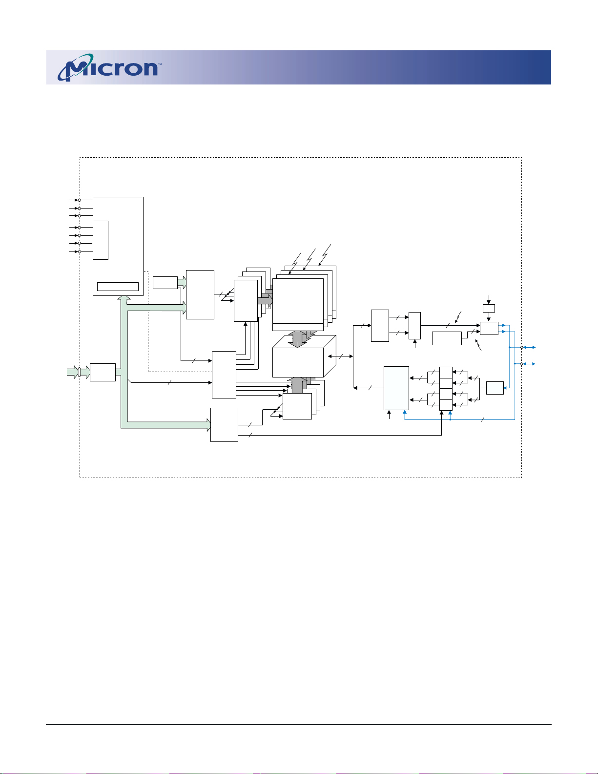
A0-A11,
BA0, BA1
CAS#
RAS#
WE#
PRELIMINARY
128Mb: x4, x8, x16
DDR SDRAM
FUNCTIONAL BLOCK DIAGRAM
32 Meg x 4
CKE
CK#
CK
DECODE
COMMAND
MODE REGISTERS
ADDRESS
REGISTER
CONTROL
LOGIC
12
REFRESH
COUNTER
12
11
BANK3
BANK2
BANK1
12
ROW-
ADDRESS
MUX
2
2
12
BANK
CONTROL
LOGIC
COLUMNADDRESS
COUNTER/
LATCH
BANK0
ROW-
ADDRESS
LATCH
&
DECODER
BANK0
4096
10
1
MEMORY
ARRAY
(4,096 x 1,024 x 8)
SENSE AMPLIFIERS
8192
I/O GATING
DM MASK LOGIC
1024
(x8)
COLUMN
DECODER
8
8
4
READ
LATCH
8
DRIVERS
ck
out
CK
WRITE
FIFO
MUX
4
COL0
MASK
&
ck
DATA
in
COL0
4
DQS
GENERATOR
INPUT
REGISTERS
1
1
2
4
8
4
CK
DLL
DATA
DRVRS
1
DQS
1
1
1
4
4
RCVRS
4
1
DQ0 DQ3, DM
DQS
CS#
14
128Mb: x4, x8, x16 DDR SDRAM Micron Technology, Inc., reserves the right to change products or specifications without notice.
128Mx4x8x16DDR_C.p65 – Rev. C; Pub. 4/01 ©2001, Micron Technology, Inc.
4
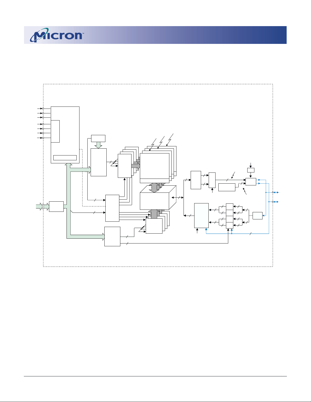
A0-A11,
BA0, BA1
CAS#
RAS#
WE#
PRELIMINARY
128Mb: x4, x8, x16
DDR SDRAM
FUNCTIONAL BLOCK DIAGRAM
16 Meg x 8
CKE
CK#
CK
DECODE
COMMAND
MODE REGISTERS
ADDRESS
REGISTER
CONTROL
LOGIC
12
REFRESH
COUNTER
12
10
BANK3
BANK2
BANK1
12
ROW-
ADDRESS
MUX
2
2
12
BANK
CONTROL
LOGIC
COLUMN-
ADDRESS
COUNTER/
LATCH
BANK0
ROW-
ADDRESS
LATCH
&
DECODER
BANK0
4096
9
1
MEMORY
ARRAY
(4,096 x 512 x 16)
SENSE AMPLIFIERS
8192
I/O GATING
DM MASK LOGIC
512
(x16)
COLUMN
DECODER
16
16
8
READ
LATCH
16
DRIVERS
ck
out
CK
WRITE
FIFO
MUX
8
COL0
MASK
&
ck
DATA
in
COL0
8
DQS
GENERATOR
INPUT
REGISTERS
1
1
2
8
16
8
CK
DLL
DATA
DRVRS
1
DQS
1
1
1
8
8
RCVRS
8
1
DQ0 DQ7, DM
DQS
CS#
14
128Mb: x4, x8, x16 DDR SDRAM Micron Technology, Inc., reserves the right to change products or specifications without notice.
128Mx4x8x16DDR_C.p65 – Rev. C; Pub. 4/01 ©2001, Micron Technology, Inc.
5
WE#
CAS#
RAS#
CKE
CK#
PRELIMINARY
128Mb: x4, x8, x16
DDR SDRAM
FUNCTIONAL BLOCK DIAGRAM
8 Meg x 16
CK
CS#
CONTROL
DECODE
COMMAND
LOGIC
REFRESH
COUNTER
12
BANK1
BANK2
BANK3
A0-A11,
BA0, BA1
14
MODE REGISTERS
ADDRESS
REGISTER
12
BANK
CONTROL
LOGIC
COLUMNADDRESS
COUNTER/
LATCH
BANK0
ROW-
ADDRESS
LATCH
&
DECODER
8
1
4096
BANK0
MEMORY
ARRAY
(4,096 x 256 x 32)
SENSE AMPLIFIERS
8192
I/O GATING
DM MASK LOGIC
256
(x32)
COLUMN
DECODER
CK
DLL
32
32
16
READ
LATCH
32
DRIVERS
ck
out
CK
WRITE
FIFO
MUX
16
COL0
MASK
4
&
32
ck
DATA
in
COL0
16
DQS
GENERATOR
INPUT
REGISTERS
2
2
16
16
DATA
2
2
16
16
DRVRS
2
DQS
2
RCVRS
16
2
DQ0 DQ15,
LDM,
UDM
LDQS
UDQS
ROW-
ADDRESS
12
12
MUX
2
2
9
128Mb: x4, x8, x16 DDR SDRAM Micron Technology, Inc., reserves the right to change products or specifications without notice.
128Mx4x8x16DDR_C.p65 – Rev. C; Pub. 4/01 ©2001, Micron Technology, Inc.
6
PRELIMINARY
128Mb: x4, x8, x16
DDR SDRAM
PIN DESCRIPTIONS
TSOP PIN NUMBERS SYMBOL TYPE DESCRIPTION
45, 46 CK, CK# Input Clock: CK and CK# are differential clock inputs. All address and
control input signals are sampled on the crossing of the positive
edge of CK and negative edge of CK#. Output data (DQs and
DQS) is referenced to the crossings of CK and CK#.
44 CKE Input Clock Enable: CKE HIGH activates and CKE LOW deactivates the
internal clock, input buffers and output drivers. Taking CKE LOW
provides PRECHARGE POWER-DOWN and SELF REFRESH
operations (all banks idle), or ACTIVE POWER-DOWN (row
ACTIVE in any bank). CKE is synchronous for POWER-DOWN
entry and exit, and for SELF REFRESH entry. CKE is asynchronous
for SELF REFRESH exit and for disabling the outputs. CKE must be
maintained HIGH throughout read and write accesses. Input
buffers (excluding CK, CK# and CKE) are disabled during POWERDOWN. Input buffers (excluding CKE) are disabled during SELF
REFRESH. CKE is an SSTL_2 input but will detect an LVCMOS
LOW level after VDD is applied.
24 CS# Input Chip Select: CS# enables (registered LOW) and disables (regis-
tered HIGH) the command decoder. All commands are masked
when CS# is registered HIGH. CS# provides for external bank
selection on systems with multiple banks. CS# is considered part
of the command code.
23, 22, 21 RAS#, CAS#, Input Command Inputs: RAS#, CAS#, and WE# (along with CS#) define the
WE# command being entered.
47 DM Input Input Data Mask: DM is an input mask signal for write data. Input
20, 47 LDM, UDM data is masked when DM is sampled HIGH along with that input data
during a WRITE access. DM is sampled on both edges of DQS.
Although DM pins are input-only, the DM loading is designed to
match that of DQ and DQS pins. For the x16 , LDM is DM for DQ0DQ7 and UDM is DM for DQ8-DQ15. Pin 20 is a NC on x4 and x8
26, 27 BA0, BA1 Input Bank Address Inputs: BA0 and BA1 define to which bank an
ACTIVE, READ, WRITE, or PRECHARGE command is being applied.
29-32, 35-40, A0–A11 Input Address Inputs: Provide the row address for ACTIVE commands, and
28, 41 the column address and auto precharge bit (A10) for READ/WRITE
commands, to select one location out of the memory array in the
respective bank. A10 sampled during a PRECHARGE command
determines whether the PRECHARGE applies to one bank (A10 LOW,
bank selected by BA0, BA1) or all banks (A10 HIGH). The address
inputs also provide the op-code during a MODE REGISTER SET
command. BA0 and BA1 define which mode register (mode register
or extended mode register) is loaded during the LOAD MODE
REGISTER command.
2, 4, 5, 7, 8, 10,11, 13, 54 DQ 0–15 I/O Data Input/Output: Data bus for x16 (4, 7, 10, 13, 54, 57, 60, and 63
56, 57, 59, 60, 62, 63,65 are NC for x8), (2, 4, 7, 8,10, 13, 54, 57, 59, 60, 63, and 65 are NC
for x4).
2, 5, 8, 11, 56, 59, 62, 65 DQ0–7 I/O Data Input/Output: Data bus for x8 (2, 8, 59, and 65 are NC for x4).
5, 11, 56, 62 DQ0 –3 I/O Data Input/Output: Data bus for x4.
(continued on next page)
128Mb: x4, x8, x16 DDR SDRAM Micron Technology, Inc., reserves the right to change products or specifications without notice.
128Mx4x8x16DDR_C.p65 – Rev. C; Pub. 4/01 ©2001, Micron Technology, Inc.
7
PRELIMINARY
128Mb: x4, x8, x16
DDR SDRAM
PIN DESCRIPTIONS (continued)
TSOP PIN NUMBERS SYMBOL TYPE DESCRIPTION
51 DQS I/O Data Strobe: Output with read data, input with write data. DQS is
16, 51 LDQS, UDQS edge-aligned with read data, centered in write data. It is used to
capture data. For the x16 , LDQS is DQS for DQ0-DQ7 and UDQS is
DQS for DQ8-DQ15. Pin 16 is NC on x4 and x8.
3, 9, 15, 55, 61 VDDQ Supply DQ Power Supply: +2.5V ±0.2V. Isolated on the die for improved
noise immunity.
6, 12, 52, 58, 64 VSSQ Supply DQ Ground. Isolated on the die for improved noise immunity.
1, 18, 33 VDD Supply Power Supply: +2.5V ±0.2V.
34, 48, 66 VSS Supply Ground.
49 VREF Supply SSTL_2 reference voltage.
14, 17, 19, 25, NC – No Connect: These pins should be left unconnected.
42, 43, 53
50 DNU – Do Not Use: Must float to minimize noise.
RESERVED NC PINS
TSOP PIN NUMBERS SYMBOL TYPE DESCRIPTION
42 A12 I Address input for 256Mb and 512Mb devices.
17 A13 I Address input for 1Gb devices.
NOTE: 1. NC pins not listed may also be reserved for other uses now or in the future. This table simply defines specific NC pins
deemed to be of importance.
1
128Mb: x4, x8, x16 DDR SDRAM Micron Technology, Inc., reserves the right to change products or specifications without notice.
128Mx4x8x16DDR_C.p65 – Rev. C; Pub. 4/01 ©2001, Micron Technology, Inc.
8

FUNCTIONAL DESCRIPTION
The 128Mb DDR SDRAM is a high-speed CMOS,
dynamic random-access memory containing
134,217,728 bits. The 128Mb DDR SDRAM is internally
configured as a quad-bank DRAM.
The 128Mb DDR SDRAM uses a double data rate
architecture to achieve high-speed operation. The
double data rate architecture is essentially a 2n-prefetch
architecture, with an interface designed to transfer two
data words per clock cycle at the I/O pins. A single read
or write access for the 128Mb DDR SDRAM consists of
a single 2n-bit wide, one-clock-cycle data transfer at the
internal DRAM core and two corresponding n-bit wide,
one-half-clock-cycle data transfers at the I/O pins.
Read and write accesses to the DDR SDRAM are
burst oriented; accesses start at a selected location and
continue for a programmed number of locations in a
programmed sequence. Accesses begin with the registration of an ACTIVE command, which is then followed by a READ or WRITE command. The address
bits registered coincident with the ACTIVE command
are used to select the bank and row to be accessed (BA0,
BA1 select the bank; A0-A11 select the row). The address bits registered coincident with the READ or WRITE
command are used to select the starting column location for the burst access.
Prior to normal operation, the DDR SDRAM must
be initialized. The following sections provide detailed
information covering device initialization, register definition, command descriptions and device operation.
Initialization
DDR SDRAMs must be powered up and initialized
in a predefined manner. Operational procedures other
than those specified may result in undefined operation. Power must first be applied to VDD and VDDQ
simultaneously, and then to VREF (and to the system
VTT). VTT must be applied after VDDQ to avoid device
latch-up, which may cause permanent damage to the
device. VREF can be applied any time after VDDQ but is
expected to be nominally coincident with VTT. Except
for CKE, inputs are not recognized as valid until after
VREF is applied. CKE is an SSTL_2 input but will detect
an LVCMOS LOW level after VDD is applied. Maintaining an LVCMOS LOW level on CKE during power-up
is required to ensure that the DQ and DQS outputs
will be in the High-Z state, where they will remain until
driven in normal operation (by a read access). After all
power supply and reference voltages are stable, and the
clock is stable, the DDR SDRAM requires a 200µs delay
prior to applying an executable command.
Once the 200µs delay has been satisfied, a DESELECT or NOP command should be applied, and CKE
should be brought HIGH. Following the NOP com-
PRELIMINARY
128Mb: x4, x8, x16
DDR SDRAM
mand, a PRECHARGE ALL command should be applied. Next a LOAD MODE REGISTER command
should be issued for the extended mode register (BA1
LOW and BA0 HIGH) to enable the DLL, followed by
another LOAD MODE REGISTER command to the
mode register (BA0/BA1 both LOW) to reset the DLL
and to program the operating parameters. Two-hundred clock cycles are required between the DLL reset
and any READ command. A PRECHARGE ALL command should then be applied, placing the device in the
all banks idle state.
Once in the idle state, two AUTO REFRESH cycles
must be performed (tRFC must be satisfied.) Additionally, a LOAD MODE REGISTER command for the
mode register with the reset DLL bit deactivated (i.e., to
program operating parameters without resetting the
DLL) is required. Following these requirements, the
DDR SDRAM is ready for normal operation.
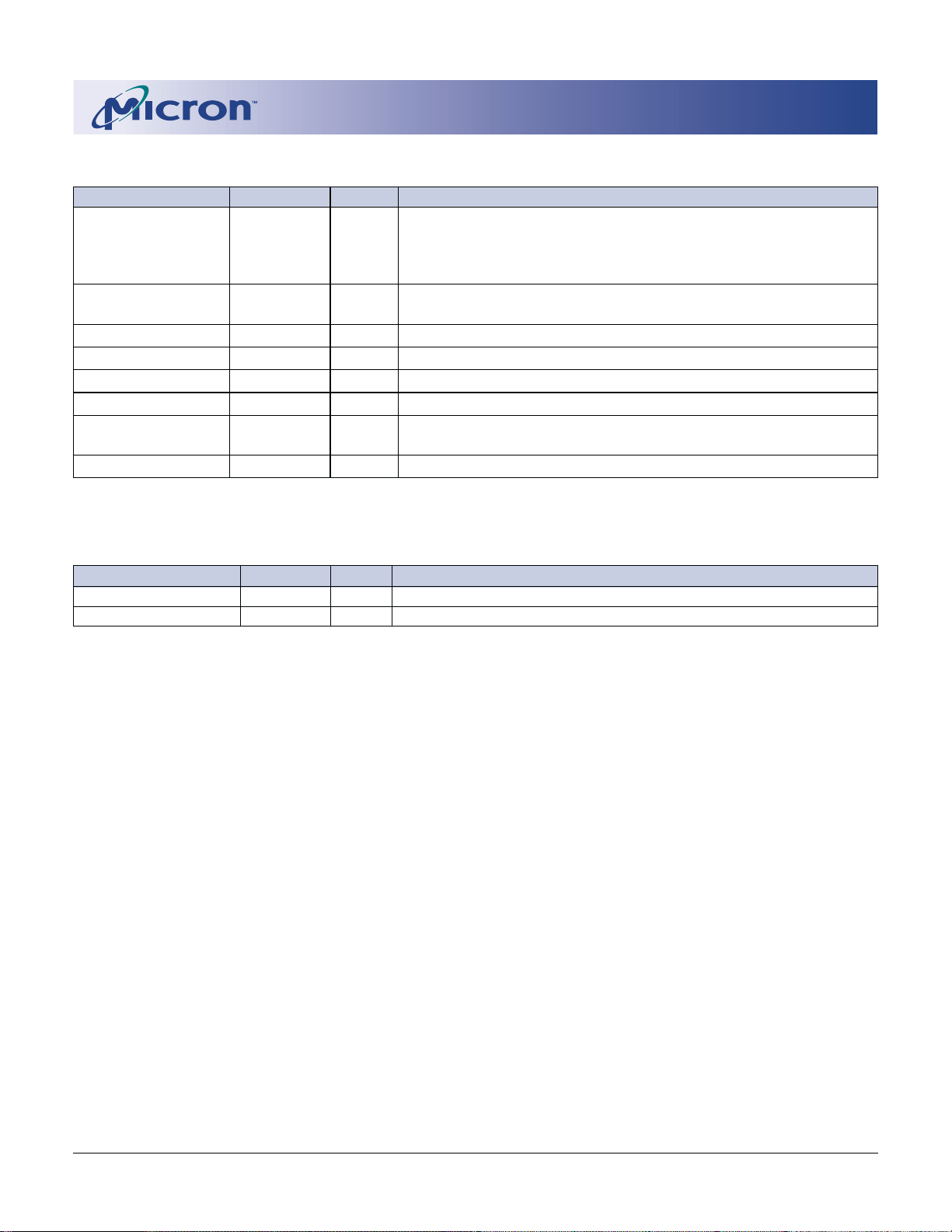
REGISTER DEFINITION
MODE REGISTER
The mode register is used to define the specific mode
of operation of the DDR SDRAM. This definition
includes the selection of a burst length, a burst type, a
CAS latency and an operating mode, as shown in
Figure 1. The mode register is programmed via the
MODE REGISTER SET command (with BA0 = 0 and
BA1 = 0) and will retain the stored information until it
is programmed again or the device loses power (except
for bit A8, which is self-clearing).
Reprogramming the mode register will not alter the
contents of the memory, provided it is performed
correctly. The mode register must be loaded (reloaded)
when all banks are idle and no bursts are in progress,
and the controller must wait the specified time before
initiating the subsequent operation. Violating either of
these requirements will result in unspecified operation.
Mode register bits A0-A2 specify the burst length, A3
specifies the type of burst (sequential or interleaved),
A4-A6 specify the CAS latency, and A7-A11 specify the
operating mode.
Burst Length
Read and write accesses to the DDR SDRAM are
burst oriented, with the burst length being programmable, as shown in Figure 1. The burst length determines the maximum number of column locations that
can be accessed for a given READ or WRITE command.
Burst lengths of 2, 4, or 8 locations are available for
both the sequential and the interleaved burst types.
128Mb: x4, x8, x16 DDR SDRAM Micron Technology, Inc., reserves the right to change products or specifications without notice.
128Mx4x8x16DDR_C.p65 – Rev. C; Pub. 4/01 ©2001, Micron Technology, Inc.
9
PRELIMINARY
128Mb: x4, x8, x16
DDR SDRAM
Reserved states should not be used, as unknown
operation or incompatibility with future versions may
result.
When a READ or WRITE command is issued, a
block of columns equal to the burst length is effectively
selected. All accesses for that burst take place within this
block, meaning that the burst will wrap within the
block if a boundary is reached. The block is uniquely
selected by A1-Ai when the burst length is set to two, by
A2-Ai when the burst length is set to four and by A3-Ai
when the burst length is set to eight (where Ai is the
most significant column address bit for a given con-
0
0
-
A7
7
M6
0
0
0
0
1
1
1
1
M10
0
0
-
A6 A5 A4
654
M4
M5
0
0
1
0
0
1
1
1
0
0
1
0
0
1
1
1
M8
M9
0
0
0
1
-
-
A3A8A2A1A0
38210
M2
M3
0
1
M7
M6-M0
0
Valid
0
Valid
-
Address Bus
Burst LengthCAS Latency BT0*0*
M1
0
0
0
0
1
1
1
1
CAS Latency
Reserved
Reserved
Reserved
Reserved
Reserved
Reserved
-
Mode Register (Mx)
Burst Length
M0
M3 = 0
0
0
Reserved
0
1
1
1
0
0
1
1
2
2.5
2
0
4
1
8
0
Reserved
1
Reserved
0
Reserved
1
Reserved
Burst Type
Sequential
Interleaved
Operating Mode
Normal Operation
Normal Operation/Reset DLL
All other states reserved
M3 = 1
Reserved
2
4
8
Reserved
Reserved
Reserved
Reserved
BA1
13
* M13 and M12 (BA0 and BA1)
must be “0, 0” to select the
base mode register (vs. the
extended mode register).
A10
BA0
A11
11
10
12
Operating Mode
A9
9
M11
Figure 1
Mode Register Definition
figuration). The remaining (least significant) address
bit(s) is (are) used to select the starting location within
the block. The programmed burst length applies to
both READ and WRITE bursts.
Burst Type
Accesses within a given burst may be programmed
to be either sequential or interleaved; this is referred to
as the burst type and is selected via bit M3.
The ordering of accesses within a burst is determined by the burst length, the burst type and the
starting column address, as shown in Table 1.
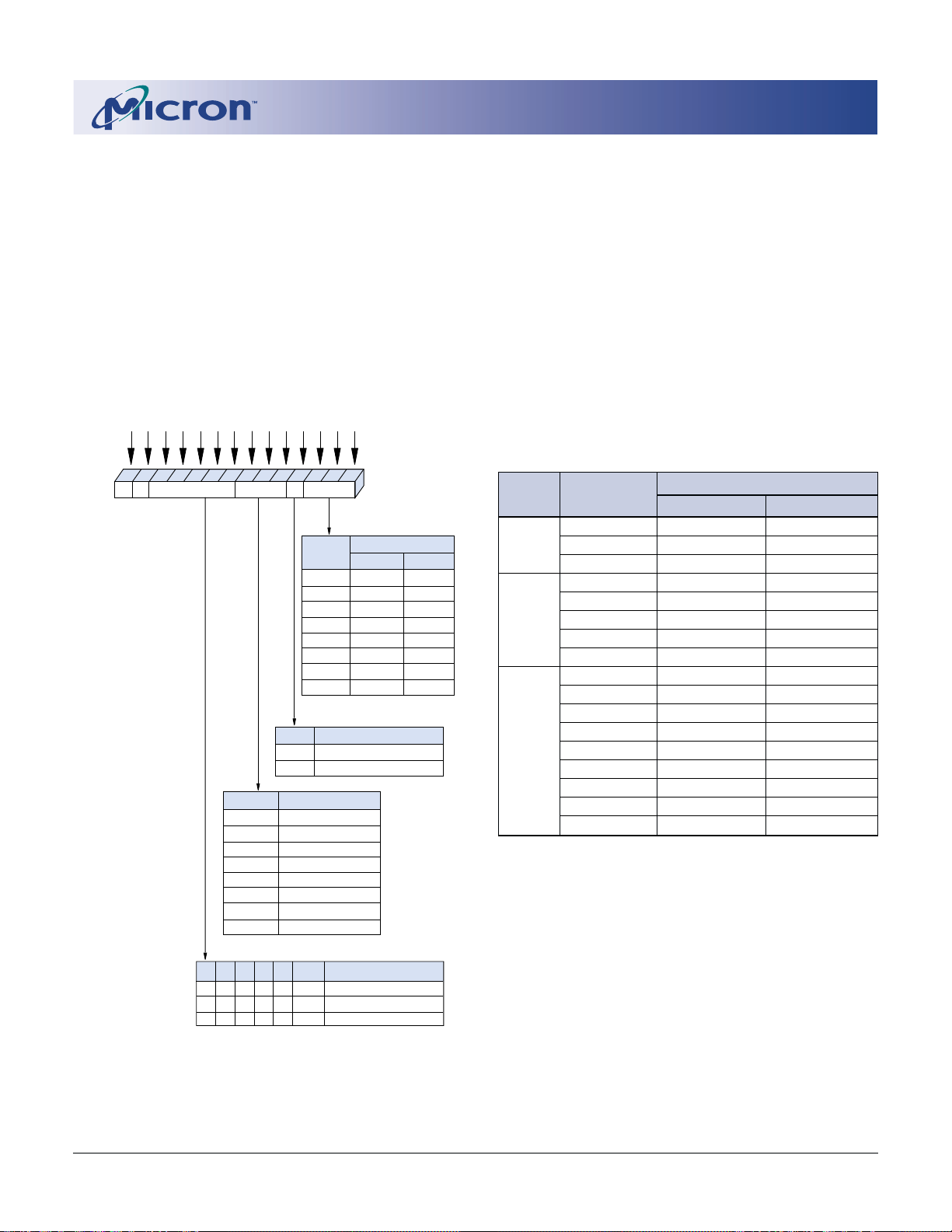
TABLE 1
BURST DEFINITION
Burst Starting Column Order of Accesses Within a Burst
Length Address Type = Sequential Type = Interleaved
A0
2
4
A2 A1 A0
0 0 0 0-1-2-3-4-5-6-7 0-1-2-3-4-5-6-7
0 0 1 1-2-3-4-5-6-7-0 1-0-3-2-5-4-7-6
0 1 0 2-3-4-5-6-7-0-1 2-3-0-1-6-7-4-5
8
0 1 1 3-4-5-6-7-0-1-2 3-2-1-0-7-6-5-4
1 0 0 4-5-6-7-0-1-2-3 4-5-6-7-0-1-2-3
1 0 1 5-6-7-0-1-2-3-4 5-4-7-6-1-0-3-2
1 1 0 6-7-0-1-2-3-4-5 6-7-4-5-2-3-0-1
1 1 1 7-0-1-2-3-4-5-6 7-6-5-4-3-2-1-0
NOTE: 1. For a burst length of two, A1-Ai select the two-
data-element block; A0 selects the first access
within the block.
2. For a burst length of four, A2-Ai select the fourdata-element block; A0-A1 select the first access
within the block.
3. For a burst length of eight, A3-Ai select the eightdata-element block; A0-A2 select the first access
within the block.
4. Whenever a boundary of the block is reached
within a given sequence above, the following
access wraps within the block.
0 0-1 0-1
1 1-0 1-0
A1 A0
0 0 0-1-2-3 0-1-2-3
0 1 1-2-3-0 1-0-3-2
1 0 2-3-0-1 2-3-0-1
1 1 3-0-1-2 3-2-1-0
128Mb: x4, x8, x16 DDR SDRAM Micron Technology, Inc., reserves the right to change products or specifications without notice.
128Mx4x8x16DDR_C.p65 – Rev. C; Pub. 4/01 ©2001, Micron Technology, Inc.
10
PRELIMINARY
128Mb: x4, x8, x16
DDR SDRAM
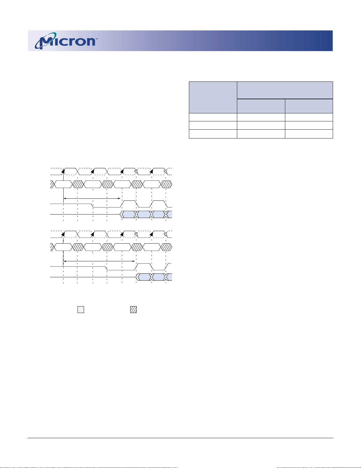
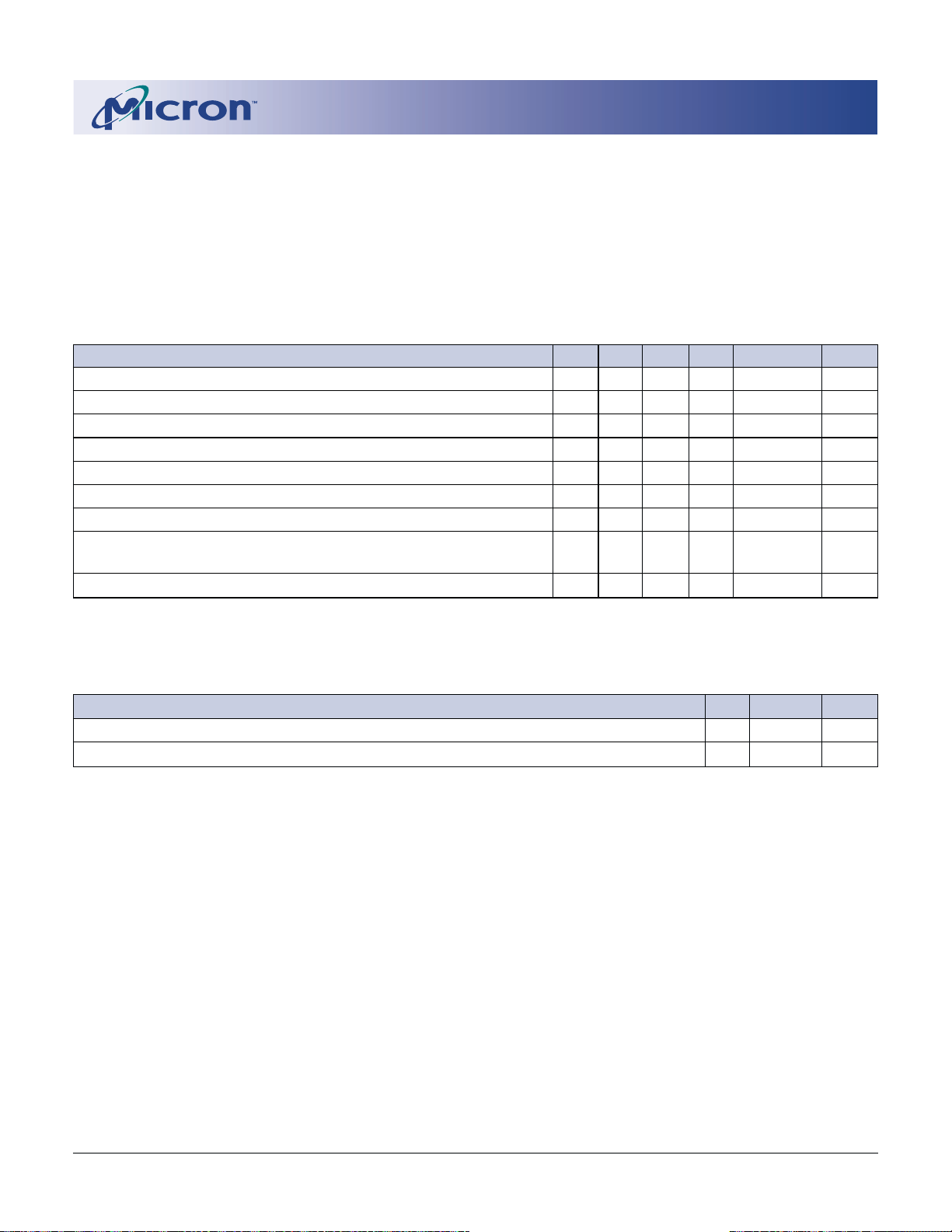
Read Latency
The READ latency is the delay, in clock cycles,
between the registration of a READ command and the
availability of the first bit of output data. The latency
can be set to 2 or 2.5 clocks, as shown in Figure 2.
If a READ command is registered at clock edge n,
and the latency is m clocks, the data will be available
nominally coincident with clock edge n + m. Table 2
indicates the operating frequencies at which each CAS
latency setting can be used.
Reserved states should not be used as unknown
operation or incompatibility with future versions may
result.
CK#
CK
COMMAND
DQS
DQ
CK#
CK
COMMAND
DQS
DQ
T0 T1 T2 T2n T3 T3n
READ NOP NOP NOP
CL = 2
T0 T1 T2 T2n T3 T3n
READ NOP NOP NOP
CL = 2.5
TABLE 2
CAS LATENCY (CL)
ALLOWABLE OPERATING
FREQUENCY (MHz)
SPEED CL = 2 CL = 2.5
-75Z 75 ≤ f ≤ 133 75 ≤ f ≤133
-75 75 ≤ f ≤ 100 75 ≤ f ≤133
-8 75 ≤ f ≤ 100 75 ≤ f ≤125
Operating Mode
The normal operating mode is selected by issuing a
MODE REGISTER SET command with bits A7-A11
each set to zero, and bits A0-A6 set to the desired values.
A DLL reset is initiated by issuing a MODE REGISTER
SET command with bits A7 and A9-A11 each set to
zero, bit A8 set to one, and bits A0-A6 set to the desired
values. Although not required by the Micron device,
JEDEC specifications recommend when a LOAD MODE
REGISTER command is issued to reset the DLL, it
should always be followed by a LOAD MODE REGISTER command to select normal operating mode.
All other combinations of values for A7-A11 are
reserved for future use and/or test modes. Test modes
and reserved states should not be used because unknown operation or incompatibility with future versions may result.
Burst Length = 4 in the cases shown
Shown with nominal tAC and nominal tDSDQ
DON’T CARETRANSITIONING DATA
Figure 2
CAS Latency
128Mb: x4, x8, x16 DDR SDRAM Micron Technology, Inc., reserves the right to change products or specifications without notice.
128Mx4x8x16DDR_C.p65 – Rev. C; Pub. 4/01 ©2001, Micron Technology, Inc.
11
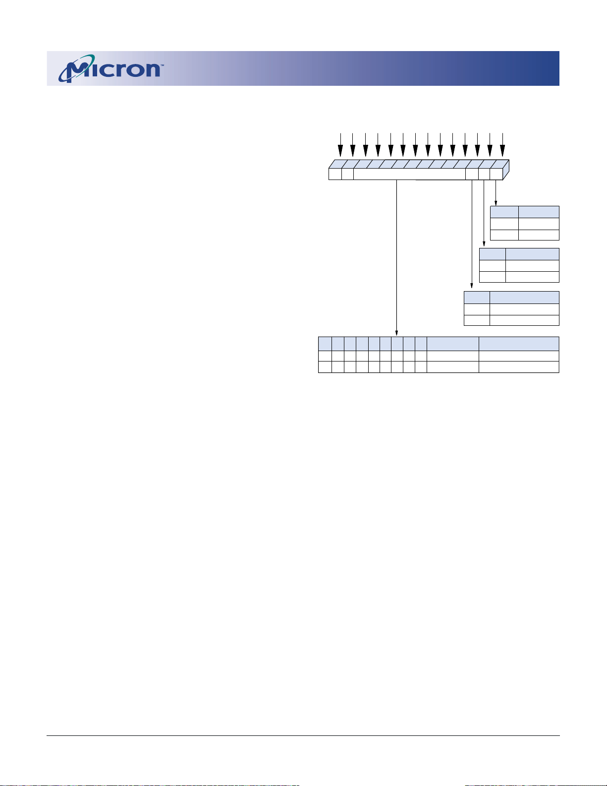
EXTENDED MODE REGISTER
Operating Mode
Normal Operation
All other states reserved
0–0
–
Valid
–
0
1
DLL
Enable
Disable
DLL
110
1
A9
A7
A6 A5 A4
A3A8A2A1A0
Extended Mode
Register (Ex)
Address Bus
9
7
654
382
1
0
E0
0
1
Drive Strength
Normal
Reduced
E1
2
0
–
QFC Function
Disabled
Reserved
E2
3
E0
E1,
Operating Mode
A10
A11
BA1
BA0
10
11
12
13
Notes: 1. E13 and E12 (BA0 and BA1) must be “1, 0” to select the
Extended Mode Register (vs. the base Mode Register).
2. The reduced drive strength option is not supported on
the x4 and x8 versions and is only available on the D3
version of the x16 device.
3. The QFC option is not supported.
E2,E3E4
0–0–0–0
–
0
–
E6E5E7E8E9
0–0
–
E10E11
DSQFC
The extended mode register controls functions
beyond those controlled by the mode register; these
additional functions are DLL enable/disable, output
drive strength, and QFC#. These functions are controlled via the bits shown in Figure 3. The extended
mode register is programmed via the LOAD MODE
REGISTER command to the mode register (with
BA0 = 1 and BA1 = 0) and will retain the stored information until it is programmed again or the device loses
power. The enabling of the DLL should always be
followed by a LOAD MODE REGISTER command to
the mode register (BA0/BA1 both LOW) to reset the DLL.
The extended mode register must be loaded when
all banks are idle and no bursts are in progress, and the
controller must wait the specified time before initiating
any subsequent operation. Violating either of these
requirements could result in unspecified operation.
Output Drive Strength
The normal full drive strength for all outputs are
specified to be SSTL2, Class II. The x16 supports an
option for reduced drive. This option is intended for
the support of the lighter load and/or point-to-point
environments. The selection of the reduced drive
strength will alter the DQs and DQSs from SSTL2, Class
II drive strength to a reduced drive strength, which is
approximately 54 percent of the SSTL2, Class II drive
strength.
The Micron 128Mb (8 Meg x16) device supports a
programmable drive strength option.
PRELIMINARY
128Mb: x4, x8, x16
DDR SDRAM
DLL Enable/Disable
The DLL must be enabled for normal operation.
DLL enable is required during power-up initialization
and upon returning to normal operation after having
disabled the DLL for the purpose of debug or evaluation. (When the device exits self refresh mode, the DLL
is enabled automatically.) Any time the DLL is enabled,
200 clock cycles must occur before a READ command
can be issued.
128Mb: x4, x8, x16 DDR SDRAM Micron Technology, Inc., reserves the right to change products or specifications without notice.
128Mx4x8x16DDR_C.p65 – Rev. C; Pub. 4/01 ©2001, Micron Technology, Inc.
Figure 3
Extended Mode Register Definition
12
PRELIMINARY
128Mb: x4, x8, x16
DDR SDRAM
Commands
Truth Table 1 provides a quick reference of available commands. This is followed by a verbal description of each command. Two additional Truth Tables
TRUTH TABLE 1 – COMMANDS
(Note: 1)
NAME (FUNCTION) CS# RAS# CAS# WE# ADDR NOTES
DESELECT (NOP) H X X X X 9
NO OPERATION (NOP) L H H H X 9
ACTIVE (Select bank and activate row) L L H H Bank/Row 3
READ (Select bank and column, and start READ burst) L H L H Bank/Col 4
WRITE (Select bank and column, and start WRITE burst) L H L L Bank/Col 4
BURST TERMINATE L H H L X 8
PRECHARGE (Deactivate row in bank or banks) L L H L Code 5
AUTO REFRESH or SELF REFRESH L L L H X 6, 7
(Enter self refresh mode)
LOAD MODE REGISTER L L L L Op-Code 2
appear following the Operation section; these tables
provide current state/next state information.
TRUTH TABLE 1A – DM OPERATION
NAME (FUNCTION) DM DQs NOTES
Write Enable L Valid 10
Write Inhibit HX 10
NOTE: 1. CKE is HIGH for all commands shown except SELF REFRESH.
2. BA0-BA1 select either the mode register or the extended mode register (BA0 = 0, BA1 = 0 select the mode register;
BA0 = 1, BA1 = 0 select extended mode register; other combinations of BA0-BA1 are reserved). A0-A11 provide the
op-code to be written to the selected mode register.
3. BA0-BA1 provide bank address and A0-A11 provide row address.
4. BA0-BA1 provide bank address; A0-Ai provide column address (where i = 8 for x16, 9 for x8, and 9, 11 for x4); A10 HIGH
enables the auto precharge feature (nonpersistent), and A10 LOW disables the auto precharge feature.
5. A10 LOW: BA0-BA1 determine which bank is precharged.
A10 HIGH: all banks are precharged and BA0-BA1 are “Don’t Care.”
6. This command is AUTO REFRESH if CKE is HIGH, SELF REFRESH if CKE is LOW.
7. Internal refresh counter controls row addressing; all inputs and I/Os are “Don’t Care” except for CKE.
8. Applies only to read bursts with auto precharge disabled; this command is undefined (and should not be used) for READ
bursts with auto precharge enabled and for WRITE bursts.
9. DESELECT and NOP are functionally interchangeable.
10. Used to mask write data; provided coincident with the corresponding data.
128Mb: x4, x8, x16 DDR SDRAM Micron Technology, Inc., reserves the right to change products or specifications without notice.
128Mx4x8x16DDR_C.p65 – Rev. C; Pub. 4/01 ©2001, Micron Technology, Inc.
13

DESELECT
The DESELECT function (CS# HIGH) prevents new
commands from being executed by the DDR SDRAM.
The DDR SDRAM is effectively deselected. Operations
already in progress are not affected.
NO OPERATION (NOP)
The NO OPERATION (NOP) command is used to
instruct the selected DDR SDRAM to perform a NOP
(CS# LOW). This prevents unwanted commands from
being registered during idle or wait states. Operations
already in progress are not affected.
LOAD MODE REGISTER
The mode registers are loaded via inputs A0-A11.
See mode register descriptions in the Register Definition section. The LOAD MODE REGISTER command
can only be issued when all banks are idle, and a
subsequent executable command cannot be issued until
t
MRD is met.
ACTIVE
The ACTIVE command is used to open (or activate)
a row in a particular bank for a subsequent access. The
value on the BA0, BA1 inputs selects the bank, and the
address provided on inputs A0-A11 selects the row.
This row remains active (or open) for accesses until a
PRECHARGE command is issued to that bank. A
PRECHARGE command must be issued before opening
a different row in the same bank.
READ
The READ command is used to initiate a burst read
access to an active row. The value on the BA0, BA1
inputs selects the bank, and the address provided on
inputs A0-Ai (where i = 8 for x16, 9 for x8, or 9, 11 for
x4) selects the starting column location. The value on
input A10 determines whether or not auto precharge is
used. If auto precharge is selected, the row being accessed will be precharged at the end of the READ burst;
if auto precharge is not selected, the row will remain
open for subsequent accesses.
WRITE
The WRITE command is used to initiate a burst write
access to an active row. The value on the BA0, BA1 inputs
selects the bank, and the address provided on inputs A0Ai (where i = 8 for x16, 9 for x8, or 9, 11 for x4) selects the
starting column location. The value on input A10 determines whether or not auto precharge is used. If auto
precharge is selected, the row being accessed will be
precharged at the end of the WRITE burst; if auto precharge
is not selected, the row will remain open for subsequent
accesses. Input data appearing on the DQs is written to
PRELIMINARY
128Mb: x4, x8, x16
DDR SDRAM
the memory array subject to the DM input logic level
appearing coincident with the data. If a given DM signal
is registered LOW, the corresponding data will be written
to memory; if the DM signal is registered HIGH, the
corresponding data inputs will be ignored, and a WRITE
will not be executed to that byte/column location.
PRECHARGE
The PRECHARGE command is used to deactivate
the open row in a particular bank or the open row in
all banks. The bank(s) will be available for a subsequent
row access a specified time (tRP) after the PRECHARGE
command is issued. Input A10 determines whether one
or all banks are to be precharged, and in the case where
only one bank is to be precharged, inputs BA0, BA1
select the bank. Otherwise BA0, BA1 are treated as
“Don’t Care.” Once a bank has been precharged, it is in
the idle state and must be activated prior to any READ
or WRITE commands being issued to that bank. A
PRECHARGE command will be treated as a NOP if
there is no open row in that bank (idle state), or if the
previously open row is already in the process of
precharging.
AUTO PRECHARGE
Auto precharge is a feature which performs the
same individual-bank precharge function described
above, but without requiring an explicit command.
This is accomplished by using A10 to enable auto
precharge in conjunction with a specific READ or
WRITE command. A precharge of the bank/row that is
addressed with the READ or WRITE command is automatically performed upon completion of the READ or
WRITE burst. Auto precharge is nonpersistent in that it
is either enabled or disabled for each individual READ
or WRITE command.
Auto precharge ensures that the precharge is initiated at the earliest valid stage within a burst. This
“earliest valid stage” is determined as if an explicit
PRECHARGE command was issued at the earliest possible time, without violating tRAS(MIN), as described
for each burst type in the Operation section of this data
sheet. The user must not issue another command to the
same bank until the precharge time (tRP) is completed.
BURST TERMINATE
The BURST TERMINATE command is used to truncate READ bursts (with auto precharge disabled). The
most recently registered READ command prior to the
BURST TERMINATE command will be truncated, as
shown in the Operation section of this data sheet. The
open page which the READ burst was terminated from
remains open.
128Mb: x4, x8, x16 DDR SDRAM Micron Technology, Inc., reserves the right to change products or specifications without notice.
128Mx4x8x16DDR_C.p65 – Rev. C; Pub. 4/01 ©2001, Micron Technology, Inc.
14

AUTO REFRESH
AUTO REFRESH is used during normal operation
of the DDR SDRAM and is analogous to CAS#-BEFORE-RAS# (CBR) REFRESH in FPM/EDO DRAMs.
This command is nonpersistent, so it must be issued
each time a refresh is required.
The addressing is generated by the internal refresh
controller. This makes the address bits a “Don’t Care”
during an AUTO REFRESH command. The 128Mb
DDR SDRAM requires AUTO REFRESH cycles at an
average interval of 15.625µs (maximum).
To allow for improved efficiency in scheduling and
switching between tasks, some flexibility in the absolute refresh interval is provided. A maximum of eight
AUTO REFRESH commands can be posted to any
given DDR SDRAM, meaning that the maximum
absolute interval between any AUTO REFRESH
command and the next AUTO REFRESH command is
9 x 15.6µs (140.6µs). This maximum absolute interval
is to allow future support for DLL updates internal
to the DDR SDRAM to be restricted to AUTO
REFRESH cycles, without allowing excessive drift in
t
AC between updates.
Although not a JEDEC requirement, to provide for
future functionality features, CKE must be active (High)
during the AUTO REFRESH period. The AUTO RE-
PRELIMINARY
128Mb: x4, x8, x16
DDR SDRAM
FRESH period begins when the AUTO REFRESH command is registered and ends
SELF REFRESH
The SELF REFRESH command can be used to retain
data in the DDR SDRAM, even if the rest of the system
is powered down. When in the self refresh mode, the
DDR SDRAM retains data without external clocking.
The SELF REFRESH command is initiated like an AUTO
REFRESH command except CKE is disabled (LOW).
The DLL is automatically disabled upon entering SELF
REFRESH and is automatically enabled upon exiting
SELF REFRESH (200 clock cycles must then occur before
a READ command can be issued). Input signals except
CKE are “Don’t Care” during SELF REFRESH.
The procedure for exiting self refresh requires a
sequence of commands. First, CK must be stable prior
to CKE going back HIGH. Once CKE is HIGH, the DDR
SDRAM must have NOP commands issued for
t
XSNR because time is required for the completion
of any internal refresh in progress. A simple algorithm
for meeting both refresh and DLL requirements is to
apply NOPs for 200 clock cycles before applying any
other command.
t
RFC later.
128Mb: x4, x8, x16 DDR SDRAM Micron Technology, Inc., reserves the right to change products or specifications without notice.
128Mx4x8x16DDR_C.p65 – Rev. C; Pub. 4/01 ©2001, Micron Technology, Inc.
15
PRELIMINARY
128Mb: x4, x8, x16
DDR SDRAM
Operations
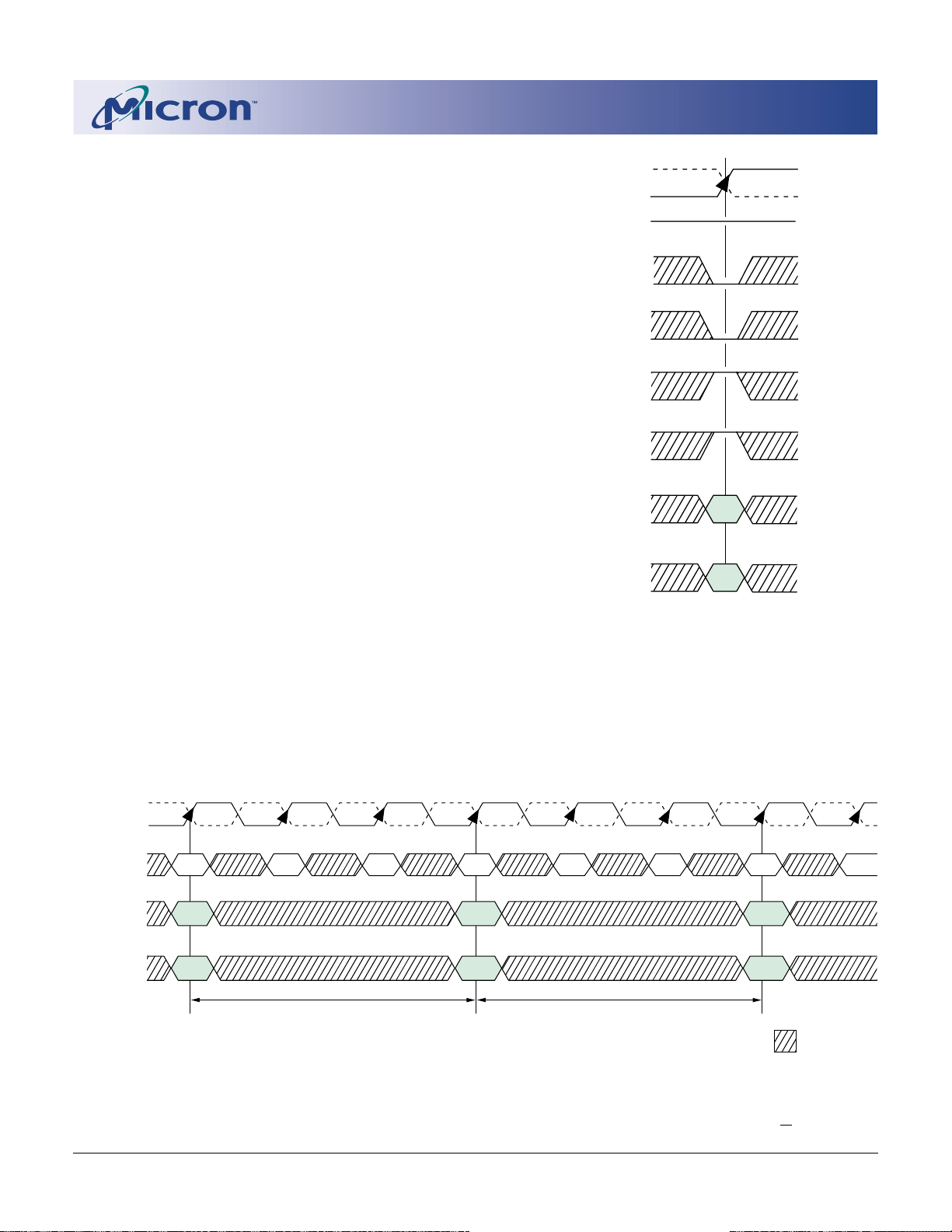
BANK/ROW ACTIVATION
Before any READ or WRITE commands can be
issued to a bank within the DDR SDRAM, a row in that
bank must be “opened.” This is accomplished via the
ACTIVE command, which selects both the bank and
the row to be activated, as shown in Figure 4.
After a row is opened with an ACTIVE command,
a READ or WRITE command may be issued to that
row, subject to the tRCD specification. tRCD (MIN)
should be divided by the clock period and rounded up
to the next whole number to determine the earliest
clock edge after the ACTIVE command on which a
READ or WRITE command can be entered. For example, a tRCD specification of 20ns with a 133 MHz
clock (7.5ns period) results in 2.7 clocks rounded to 3.
This is reflected in Figure 5, which covers any case where
2 < tRCD (MIN)/tCK ≤ 3. (Figure 5 also shows the same
case for tRCD; the same procedure is used to convert
other specification limits from time units to clock
cycles).
A subsequent ACTIVE command to a different row
in the same bank can only be issued after the previous
active row has been “closed” (precharged). The minimum time interval between successive ACTIVE commands to the same bank is defined by tRC.
A subsequent ACTIVE command to another bank
can be issued while the first bank is being accessed,
which results in a reduction of total row-access overhead. The minimum time interval between successive
ACTIVE commands to different banks is defined by
t
RRD.
CK#
CK
CKE
HIGH
CS#
RAS#
CAS#
WE#
A0-A11
BA0,1
RA
BA
RA = Row Address
BA = Bank Address
Figure 4
Activating a Specific Row in
a Specific Bank
CK#
CK
COMMAND
A0-A11
BA0, BA1
T0 T1 T2 T3 T4 T5 T6 T7
ACT ACT
Row Row
Bank x Bank y
NOP
t
NOP
RRD
NOP
t
NOP
RCD
RD/WR
Col
Bank y
DON’T CARE
NOP
Figure 5
Example: Meeting tRCD (tRRD) MIN When 2 < tRCD (tRRD) MIN/tCK < 3
128Mb: x4, x8, x16 DDR SDRAM Micron Technology, Inc., reserves the right to change products or specifications without notice.
128Mx4x8x16DDR_C.p65 – Rev. C; Pub. 4/01 ©2001, Micron Technology, Inc.
16
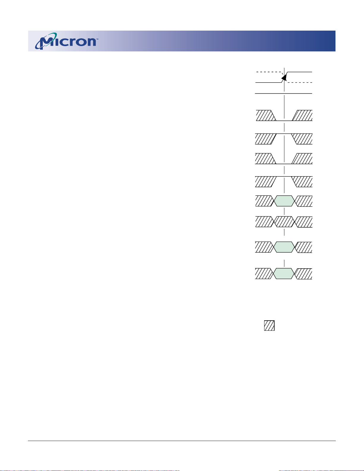
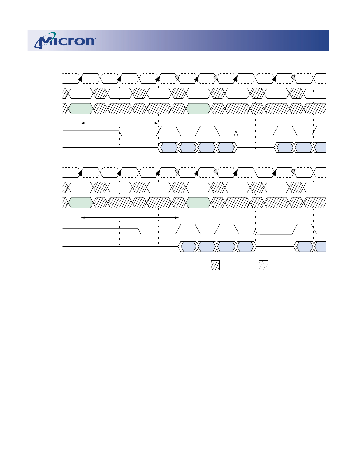
READS
READ bursts are initiated with a READ command,
as shown in Figure 6.
The starting column and bank addresses are provided with the READ command and auto precharge is
either enabled or disabled for that burst access. If auto
precharge is enabled, the row being accessed is
precharged at the completion of the burst. For the
generic READ commands used in the following illustrations, auto precharge is disabled.
During READ bursts, the valid data-out element
from the starting column address will be available
following the CAS latency after the READ command.
Each subsequent data-out element will be valid nominally at the next positive or negative clock edge (i.e., at
the next crossing of CK and CK#). Figure 7 shows
general timing for each possible CAS latency setting.
DQS is driven by the DDR SDRAM along with output
data. The initial LOW state on DQS is known as the
read preamble; the LOW state coincident with the last
data-out element is known as the read postamble.
Upon completion of a burst, assuming no other
commands have been initiated, the DQs will go
High-Z. A detailed explanation of tDQSQ (valid dataout skew), tQH (data-out window hold), the valid
data window are depicted in Figure 27. A detailed
explanation of tDQSCK (DQS transition skew to CK)
and tAC (data-out transition skew to CK) is depicted in
Figure 28.
Data from any READ burst may be concatenated
with or truncated with data from a subsequent READ
command. In either case, a continuous flow of data
can be maintained. The first data element from the new
burst follows either the last element of a completed
burst or the last desired data element of a longer burst
which is being truncated. The new READ command
should be issued x cycles after the first READ command,
where x equals the number of desired data element
pairs (pairs are required by the 2n-prefetch architecture). This is shown in Figure 8. A READ command can
be initiated on any clock cycle following a previous
READ command. Nonconsecutive read data is shown
for illustration in Figure 9. Full-speed random read
accesses within a page (or pages) can be performed as
shown in Figure 10.
CK#
CK
CKE
CS#
RAS#
CAS#
WE#
x4: A0–A9, A11
x8: A0–A9
x16: A0–A8
x8: A11
x16: A9, A11
A10
BA0,1
CA = Column Address
BA = Bank Address
EN AP = Enable Auto Precharge
DIS AP = Disable Auto Precharge
READ Command
PRELIMINARY
128Mb: x4, x8, x16
DDR SDRAM
HIGH
CA
EN AP
DIS AP
BA
DON’T CARE
Figure 6
128Mb: x4, x8, x16 DDR SDRAM Micron Technology, Inc., reserves the right to change products or specifications without notice.
128Mx4x8x16DDR_C.p65 – Rev. C; Pub. 4/01 ©2001, Micron Technology, Inc.
17
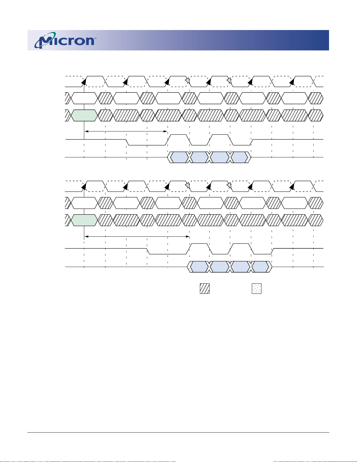
CK#
CK
PRELIMINARY
128Mb: x4, x8, x16
DDR SDRAM
T0 T1 T2 T3T2n T3n T4 T5
COMMAND
ADDRESS
DQS
DQ
CK#
CK
COMMAND
ADDRESS
DQS
DQ
READ NOP NOP NOP NOP NOP
Bank a,
Col n
CL = 2
DO
n
T0 T1 T2 T3T2n T3n T4 T5
READ NOP NOP NOP NOP NOP
Bank a,
Col n
CL = 2.5
DO
n
NOTE: 1. DO n = data-out from column n.
DON’T CARE TRANSITIONING DATA
2. Burst length = 4.
3. Three subsequent elements of data-out appear in the programmed order following DO n.
4. Shown with nominal tAC, tDQSCK, and tDQSQ.
Figure 7
READ Burst
128Mb: x4, x8, x16 DDR SDRAM Micron Technology, Inc., reserves the right to change products or specifications without notice.
128Mx4x8x16DDR_C.p65 – Rev. C; Pub. 4/01 ©2001, Micron Technology, Inc.
18

PRELIMINARY
128Mb: x4, x8, x16
DDR SDRAM
CK#
CK
COMMAND
ADDRESS
DQS
DQ
CK#
CK
COMMAND
COMMAND
ADDRESS
ADDRESS
T0 T1 T2 T3T2n T3n T4 T5T4n T5n
READ NOP READ NOP NOP NOP
Bank,
Col n
Bank,
Col b
CL = 2
DO
n
DO
b
T0 T1 T2 T3T2n T3n T4 T5T4n T5n
READ NOP READ NOP NOP NOP
Bank,
Col n
Bank,
Col b
CL = 2.5
DQS
DQ
DO
n
DO
b
DON’T CARE TRANSITIONING DATA
NOTE: 1. DO n (or b) = data-out from column n (or column b).
2. Burst length = 4 or 8 (if 4, the bursts are concatenated; if 8, the second burst interrupts the first).
3. Three subsequent elements of data-out appear in the programmed order following DO n.
4. Three (or seven) subsequent elements of data-out appear in the programmed order following DO b.
5. Shown with nominal
t
AC, tDQSCK, and tDQSQ.
6. Example applies only when READ commands are issued to same device.
Figure 8
Consecutive READ Bursts
128Mb: x4, x8, x16 DDR SDRAM Micron Technology, Inc., reserves the right to change products or specifications without notice.
128Mx4x8x16DDR_C.p65 – Rev. C; Pub. 4/01 ©2001, Micron Technology, Inc.
19
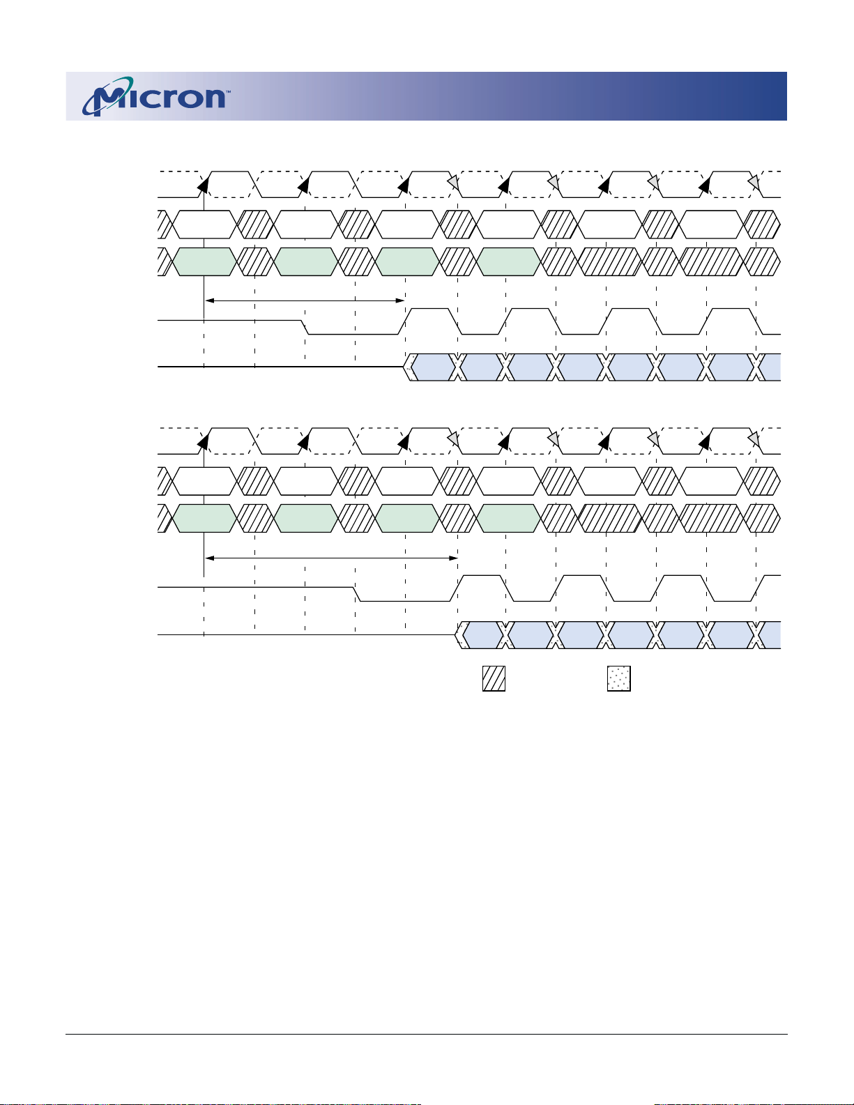
PRELIMINARY
128Mb: x4, x8, x16
DDR SDRAM
CK#
CK
COMMAND
ADDRESS
DQS
DQ
CK#
CK
COMMAND
COMMAND
ADDRESS
ADDRESS
DQS
T0 T1 T2 T3T2n T3n T4 T5 T5n T6
READ NOP NOP NOP NOP NOP
Bank,
Col n
READ
Bank,
Col b
CL = 2
DO
n
DO
b
T0 T1 T2 T3T2n T3n T4 T5 T5n T6
READ NOP NOP NOP NOP NOP
Bank,
Col n
READ
Bank,
Col b
CL = 2.5
DQ
DO
n
DO
b
DON’T CARE TRANSITIONING DATA
NOTE: 1. DO n (or b) = data-out from column n (or column b).
2. Burst length = 4 or 8 (if 4, the bursts are concatenated; if 8, the second burst interrupts the first).
3. Three subsequent elements of data-out appear in the programmed order following DO n.
4. Three (or seven) subsequent elements of data-out appear in the programmed order following DO b.
5. Shown with nominal
t
AC, tDQSCK, and tDQSQ.
6. Example applies when READ commands are issued to different devices or nonconsecutive READs.
Figure 9
Nonconsecutive READ Bursts
128Mb: x4, x8, x16 DDR SDRAM Micron Technology, Inc., reserves the right to change products or specifications without notice.
128Mx4x8x16DDR_C.p65 – Rev. C; Pub. 4/01 ©2001, Micron Technology, Inc.
20
CK#
CK
PRELIMINARY
128Mb: x4, x8, x16
DDR SDRAM
T0 T1 T2 T3T2n T3n T4 T5T4n T5n
COMMAND
ADDRESS
DQS
DQ
CK#
CK
COMMAND
COMMAND
ADDRESS
ADDRESS
DQS
READ READ READ NOP NOP
Bank,
Col n
Bank,
Col x
Bank,
Col b
READ
Bank,
Col g
CL = 2
DO
n
DO
n'
DO
x
DO
x'
DO
b
DO
b'
DO
g
T0 T1 T2 T3T2n T3n T4 T5T4n T5n
READ READ READ NOP NOP
Bank,
Col n
Bank,
Col x
Bank,
Col b
READ
Bank,
Col g
CL = 2.5
DQ
DO
n
DO
n'
DO
x
DO
x'
DO
b
DO
b'
DON’T CARE TRANSITIONING DATA
NOTE: 1. DO n (or x or b or g) = data-out from column n (or column x or column b or column g).
2. Burst length = 2 or 4 or 8 (if 4 or 8, the following burst interrupts the previous).
3. n' or x' or b' or g' indicates the next data-out following DO n or DO x or DO b or DO g, respectively.
4. READs are to an active row in any bank.
t
5. Shown with nominal
AC, tDQSCK, and tDQSQ.
Figure 10
Random READ Accesses
128Mb: x4, x8, x16 DDR SDRAM Micron Technology, Inc., reserves the right to change products or specifications without notice.
128Mx4x8x16DDR_C.p65 – Rev. C; Pub. 4/01 ©2001, Micron Technology, Inc.
21
 Loading...