

Page 1

Technical Note
GDDR6: Design Guide
Introduction
GDDR6 is a high-speed synchronous dynamic random-access (SDRAM) memory designed to support applications requiring high bandwidth such as graphic cards, game
consoles, and high-performance compute systems, as well as emerging applications
that demand even higher memory bandwidth.
In addition to standard graphics GDDR6, Micron offers two additional GDDR6 devices:
GDDR6 networking (GDDR6N) and GDDR6 automotive. GDDR6N is targeted at networking and enterprise-class applications. GDDR6 automotive is targeted for automotive requirements and processes. All three Micron GDDR6 devices have been designed
and tested to meet the needs of their specific applications for bandwidth, reliability and
longevity.
This technical note is designed to help readers implement GDDR6 as an off-the-shelf
memory with established packaging, handling and testing. It outlines best practices for
signal and power integrity, as well as standard GDDR6 DRAM features, to help new system designs achieve the high data rates offered by GDDR6.
TN-ED-04: GDDR6 Design Guide
Introduction
CCM005-524338224-10517
tn_ed_04_gddr6_design_guide.pdf - Rev. B 1/2021 EN
Products and specifications discussed herein are for evaluation and reference purposes only and are subject to change by
Micron without notice. Products are only warranted by Micron to meet Micron's production data sheet specifications. All
information discussed herein is provided on an "as is" basis, without warranties of any kind.
1
Micron Technology, Inc. reserves the right to change products or specifications without notice.
© 2018 Micron Technology, Inc. All rights reserved.
Page 2
GDDR6 Overview
TN-ED-04: GDDR6 Design Guide
GDDR6 Overview
In the DRAM evolutionary process, GDDR6 has made a significant leap in throughput
while maintaining standard packaging and assembly processes. While standard DRAM
speeds have continued to increase, development focus has been primarily on density —
often at the expense of bandwidth. GDDR has taken a different path, focusing on high
bandwidth. With DDR4 operating from 1.6 to 3.2 Gb/s, LPDDR4 up to 4.2 Gb/s, and
GDDR5N at 6 Gb/s, the increase in clock and data speeds has made it important to follow good design practices. Now, with GDDR6 speeds reaching 14 Gb/s and beyond, it is
critical to have designs that are well planned, simulated and implemented.
GDDR6 DRAM is high-speed memory designed specifically for applications requiring
high bandwidth. In addition to graphics, Micron GDDR6 is offered in networking
(GDDR6N) and automotive grades, sharing similar targets for extended reliability and
longevity. For the networking and automotive grade devices, maximum data rate and
voltage supply differ slightly from Micron graphics GDDR6 to help assure long-term reliability; all other aspects between Micron GDDR6, GDDR6N and GDDR6 automotive
are the same. All content discussed in this technical note applies equally to all GDDR6
products. 12 Gb/s will be used for examples, although higher rates may be available.
GDDR6 has 32 data pins, designed to operate as two independent x16 channels. It can
also operate as a single x32 (pseudo-channel) interface. A GDDR6 channel is point to
point, single DQ load. Designed for single rank only, with no allowances for multiple
rank configurations. Internally, the device is configured as a 16-bank DRAM and uses a
16n-prefetch architecture to achieve high-speed operation. The 16n-prefetch architecture is combined with an interface designed to transfer 8 data words per clock cycle at
the I/O pins.
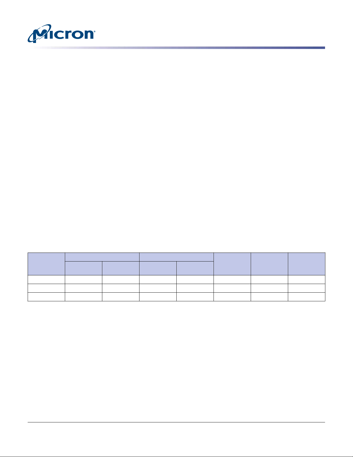
Table 1: Micron GDDR and DDR4 DRAM Comparison
Clock Period (tCK) Data Rate (Gb/s)
Product
DDR4 1.25ns 0.625ns 1.6 3.2 4–16Gb 8n 8, 16
GDDR5 20ns 1.00ns 2 8 4–8Gb 8n 16
GDDR6 20ns 0.571ns 2 14 8–16Gb 16n 16
Density
Prefetch
(Burst
Length)
Number of
BanksMAX MIN MIN MAX
For more information, see the Micron GDDR6 The Next-Generation Graphics DRAM
technical note (TN-ED-03) available on micron.com.
Density
The JEDEC® standard for GDDR6 DRAM defines densities from 8Gb, 12Gb, 16Gb, 24Gb
to 32Gb. At the time of publication of this technical note, Micron supports 8Gb and
16Gb parts.
For applications that require higher density, GDDR6 can operate two devices on a single
channel (see Channel Options later in this document or the Micron GDDR6 data sheet
for details).
CCM005-524338224-10517
tn_ed_04_gddr6_design_guide.pdf - Rev. B 1/2021 EN
2
Micron Technology, Inc. reserves the right to change products or specifications without notice.
© 2018 Micron Technology, Inc. All rights reserved.
Page 3
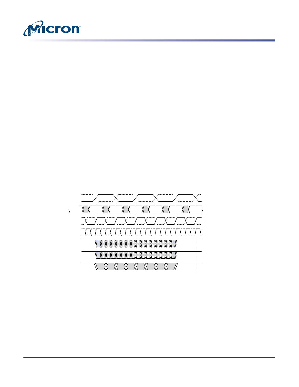
Prefetch
CK
DQ,DBI_n
EDC
WCK
WCK
f (e.g. 1.5 GHz)
2f (e.g. 3 Gb/s)
2f (e.g. 3 GHz)
4f (e.g. 6 GHz)
8f (e.g. 12 Gb/s)
4f (e.g. 6 Gb/s)
CA
8f (e.g. 12 Gb/s)
EDC
(quad data rate)
(full data rate)
(half data rate)
(double data rate)
Frequency
TN-ED-04: GDDR6 Design Guide
GDDR6 Overview
Prefetch (burst length) is 16n, double that of GDDR5. GDDR5X was the first GDDR to
change to 16n prefetch, which, along with the 32-bit wide interface, meant an access
granularity of 64 bytes. GDDR6 now allows flexibility in access size by using two 16-bit
channels, each with a separate command and address. This allows each 16-bit channel
to have a 32-byte access granularity — the same as GDDR5.
Micron GDDR6N and GDDR6 automotive have been introduced with data rates of 10
Gb/s and 12 Gb/s (per pin). The JEDEC GDDR6 standard does not define AC timing parameters or clock speeds. Micron GDDR6 is initially available up to 14 Gb/s. Micron's
paper, 16 Gb/s and Beyond with Single-Ended I/O in High-Performance Graphics Memo-
ry, describes GDDR6 DRAM operation up to 16 Gb/s, and the possibility of operating
the data interface as high as 20 Gb/s (demonstrated on the interface only; the memory
array itself was not tested to this speed).
GDDR6 data frequency is 8X the input reference clock and 4X the WCK data clock frequency. WCK is provided by the host. The system should always be capable to provide
four WCK signals. (WCK per byte). Though not required by all DRAM, ability to supply
four WCK signals ensures compatibility with all GDDR6 components.
Figure 1: WCK Clocking Frequency and EDC Pin Data Rate Options (Example)
For more information on clocking speeds and options, see the Micron GDDR6 The
Next-Generation Graphics DRAM technical note (TN-ED-03) and the GDDR6N data
sheet (available upon request) on micron.com.
CCM005-524338224-10517
tn_ed_04_gddr6_design_guide.pdf - Rev. B 1/2021 EN
3
Micron Technology, Inc. reserves the right to change products or specifications without notice.
© 2018 Micron Technology, Inc. All rights reserved.
Page 4
Command Address
Bus Inversion
TN-ED-04: GDDR6 Design Guide
GDDR6 Overview
GDDR6 has a new “packetized” command address (CA) bus. Command and address are
combined into a single, 10-bit interface, operating at double data rate to CK. This eliminates chip select, address strobe, and write enable signals and minimizes the required
CA pin count to 12 per channel (or 16 in pseudo-channel mode). The elimination of a
CS aligns with the point-to-point nature of GDDR memory and reinforces the requirement that there is only a single (logical) device per memory interface (single DRAM or
two DRAM back-to-back in byte mode, operating as a single addressable memory).
As shown in the clock diagram, CA operates at double CK. The first half of command/
address is latched on the rising edge, and the second half of command/address is latched on the falling edge. Refer to the Command Truth Table in the product data sheet for
encoding of each command.
• DDR packetized CA bus CA[9:0] replaces the 15 command address signals used in
GDDR5.
• Command address bus inversion limits the number of CA bits driving low to 5, or 7, in
PC mode.
Data bus inversion (DBI) and command address bus inversion (CABI) are enabled in
mode register 1. Although optional, DBI and CABI are critical to high-speed signal integrity and are required for operation at full speed.
DBI is used in GDDR5 as well as DDR4, and CABI leverages address bus inversion (ABI)
from GDDR5. DBI and CABI:
• Drive fewer bits LOW (maximum of half of the bits are driven LOW, including the
DBI_n pin)
• Consume less power (only bits that are driven LOW consume power)
• Result in less noise and better data eye
• Apply to both READ and WRITE operations, which can be enabled separately
READ WRITE
If more than four bits of a byte are LOW:
— Invert output data
— Drive DBI_n pin LOW
If four or less bits of a byte lane are LOW:
— Do not invert output data
— Drive DBI_n pin HIGH
CRC Data Link Protection
GDDR6 provides data bus protection in the form of CRC. Micron GDDR6N supports
half or full data rate EDC function. At half rate, an 8-bit checksum is created per write or
read burst. The checksum uses a similar polynomial as the full data rate option to calculate two intermediate 8-bit checksums, and then compresses these two into a final 8-bit
checksum. This allows 100% fault detection coverage for random single, double and triple bit errors, and >99% fault detection for other random errors. The nature of the EDC
signal is such that it is always sourced from DRAM to controller, for both reads and
writes. Due to this, extra care is recommended during PCB design and analysis ensuring
the EDC net is evaluated for both near-end and far-end crosstalk.
If DBI_n input is LOW, write data is inverted
— Invert data internally before storage
If DBI_n input is HIGH, write data is not inverted
CCM005-524338224-10517
tn_ed_04_gddr6_design_guide.pdf - Rev. B 1/2021 EN
4
Micron Technology, Inc. reserves the right to change products or specifications without notice.
© 2018 Micron Technology, Inc. All rights reserved.
Page 5

Banks and Bank Grouping
Refer to Micron product data sheets for currently available speed grades and bank
grouping requirements.
Micron GDDR6 supports bank groups as defined in the JEDEC specification. Bank
groups are enabled through MR3; it is recommended that bank groups are disabled if
not required for the desired frequency of operation. Short timings are supported without bank groups. Enabling bank groups in MR3 will have no benefit, and results in a
small timing penalty by requiring use of tRRDL, tCCDL, tWTRL and tRTPL.
• GDDR6 has 16 banks.
• With bank groups enabled, organized as four bank groups, each comprised of four
sub-banks, per JEDEC.
• Maximum clock frequency with bank groups disabled is (fCKBG). Refer to product
specific data sheets for fCKBG specifications.
VPP Supply
VPP input—added with GDDR5X—is a 1.8V supply that powers the internal word line.
Adding the VPP supply facilitates the VDD transition to 1.35V and 1.25V and provides additional power savings. It is worth keeping in mind that IPP values are average currents,
and actual current draw will be narrow pulses in nature. Failure to provide sufficient
power to VPP prevents the DRAM from operating correctly.
TN-ED-04: GDDR6 Design Guide
GDDR6 Overview
V
REFC
V
REFD
POD I/O Buffers
GDDR6 has the option to use internal V
sults with good accuracy as well as allowing adjustability. V
× V
that the V
V
. External V
DDQ
input should be pulled to VSS using a zero ohm resistor.
REFC
is internally generated by the DRAM. V
REFD
is also acceptable. If internal V
REFC
. This method should provide optimum re-
REFC
has a default level of 0.7
REFC
is used, it is recommended
REFC
is now independent per data pin and
REFD
can be set to any value over a wide range. This means the DRAM controller must set the
DRAM’s V
settings to the proper value; thus, V
REFD
must be trained.
REFD
The I/O buffer is pseudo open drain (POD), as seen in the figure below. By being terminated to V
instead of half of V
DDQ
, the size and center of the signal swing can be cus-
DDQ
tom-tailored to each design’s need. POD enables reduced switching current when driving data since only zeros consume power, and additional switching current savings can
be realized with DBI enabled. An additional benefit with DBI enabled is a reduction in
switching noise resulting in a larger data-eye.
If not configured otherwise, termination and drive strength are automatically calibrated
within the selected range using the ZQ resistor. It is also possible to specify an offset or
disable the automatic calibration. It is expected that the system should perform optimally with auto calibration enabled.
CCM005-524338224-10517
tn_ed_04_gddr6_design_guide.pdf - Rev. B 1/2021 EN
5
Micron Technology, Inc. reserves the right to change products or specifications without notice.
© 2018 Micron Technology, Inc. All rights reserved.
Page 6
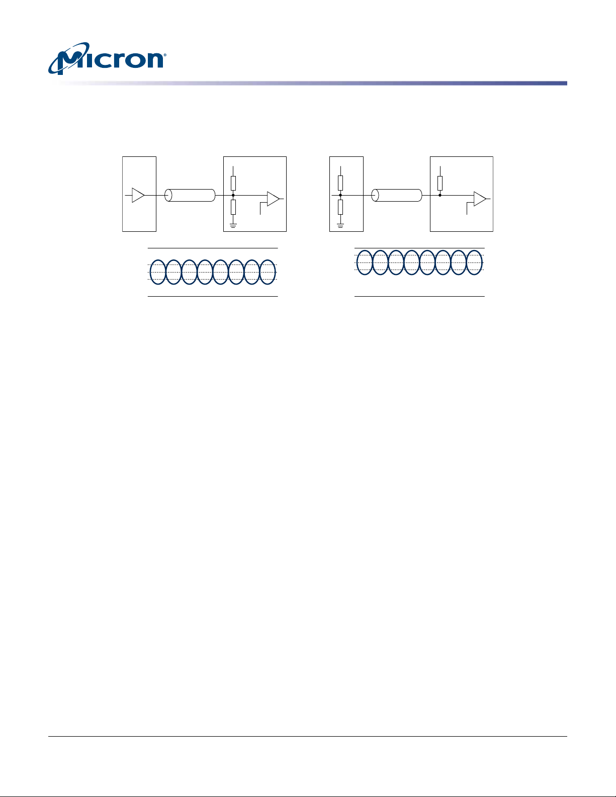
Figure 2: Signaling Schemes
SSTL POD15/POD125/POD135
TX
Z
V
REF
=
0.5 × V
DDQ
V
REF
=
0.7 × V
DDQ
V
DDQ
V
DDQ
V
DDQ
2 × R
TT
2 × R
TT
RX TX
Z
60Ω
RX
V
REF
V
DDQ
V
SSQ
V
IH
V
IL
V
REF
V
DDQ
V
SSQ
V
IH
V
IL
60Ω
40Ω
Clock Termination
GDDR6 includes the ability to apply ODT on CK_t/CK_c. The clock ODT configuration
is selected at reset initialization. Refer to Device Initialization in the product data sheet
for available modes and requirements. If ODT is not used, the clock signals should be
terminated on the PCB (similar to GDDR5), with CK_t and CK_c terminated independently (single-ended) to V
DDQ
TN-ED-04: GDDR6 Design Guide
GDDR6 Overview
.
JTAG Signals
GDDR6 includes boundary scan functionality to assist in testing. It is recommended to
take advantage of this capability if possible in the system. In addition to IO testing,
boundary scan can be used to read device temperature and V
system-wide JTAG, it might be considered to connect JTAG to test points or connector
for possible later use. If unused, the four JTAG signals are ok to float. TDO is High-Z by
default. TMS, TDI, and TCK have internal pull-ups. If pins are connected, a pull-up can
be installed on TMS to help ensure it remains inactive.
values. If there is no
REFD
CCM005-524338224-10517
tn_ed_04_gddr6_design_guide.pdf - Rev. B 1/2021 EN
6
Micron Technology, Inc. reserves the right to change products or specifications without notice.
© 2018 Micron Technology, Inc. All rights reserved.
Page 7

Channel Options
GDDR6 has the flexibility to operate the command and address busses in four different
configurations, allowing the device to be optimized for application-specific requirements:
• x16 mode (two independent x16 bit data channels)
• x8 mode (two devices, each with x8 channels, in a back-to-back "clamshell" configuration)
• 2-channel mode (two independent command/address busses)
• Pseudo channel (PC) mode (a single CA bus and combined x32 data bus; similar to
GDDR5 and GDDR5X)
These are configured by pin state during reset initialization (during initialization, the
pins are sampled to configure the options). The controller must meet device setup and
hold times (specified in the data sheet) prior to de-assertion of RESET_n (tATS and
t
ATH).
x16 Mode/x8 Mode (Clamshell)
GDDR6 standard mode of operation is x16 mode, providing two 16-bit channels. It is also possible to configure the device in a mode that provides two 8-bit wide channels for
clamshell configuration. This option puts each of the clamshell devices into a mode
where only half of each channel is used from each component (hence, the x8 designation).
TN-ED-04: GDDR6 Design Guide
Channel Options
• To be used for creating a clamshell (back-to-back) pair of two devices operating as a
single memory.
• Allows for a doubling of density. Two 8Gb devices appear to the controller as a single,
logical 16Gb device with two 16-bite wide channels.
• Configured by state of EDC1_A and EDC0_B, tied to VSS, at the time RESET_n is deasserted.
• One byte of each device is disabled and can be left floating (NC). Along with DQs for
the byte, DBI_n is also disabled, in High-Z state.
• Separate WCK must be provided for each byte. (WCK per word cannot be used in this
configuration)
2-Channel Mode/Pseudo Channel Mode
• 2-channel mode is the standard mode of operation for GDDR6. It is expected to return better performance in most cases.
• Configured by state of CA6_A and CA6_B at the time RESET_n is deasserted.
• The difference in CA bus pin usage between PC mode and 2-channel mode is that 8 of
the 12 CA pins (CKE_n, CA[9:4], CABI_n) are shared between both channels, while only the other four CA pins (CA[3:0]) are routed separately for each channel (similar to
GDDR5X operation).
CCM005-524338224-10517
tn_ed_04_gddr6_design_guide.pdf - Rev. B 1/2021 EN
7
Micron Technology, Inc. reserves the right to change products or specifications without notice.
© 2018 Micron Technology, Inc. All rights reserved.
Page 8
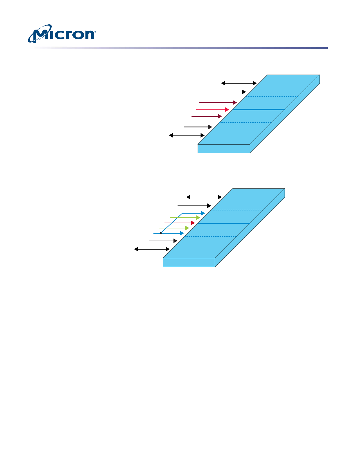
Figure 3: GDDR6 Pins in 2-Channel Mode
DQ[15:0],DBI[1:0]_n,EDC[1:0]
GDDR6
Bytes 0+1
Bytes 0 + 1
Control B
DQ[15:0],DBI[1:0]_n,EDC[1:0]
CKE_n,CA[9:0],CABI_n
Channel B
Channel A
Control A
CK_t/_c
CKE_n,CA[9:0],CABI_n
WCK0_t/_c,WCK1_t/_c
WCK0_t/_c,WCK1_t/_c
GDDR6
Bytes 0+1
Bytes 0 + 1
Control B
DQ[15:0],DBI[1:0]_n,EDC[1:0]
DQ[15:0],DBI[1:0]_n,EDC[1:0]
CA[3:0]
CA[3:0]
Channel B
Channel A
Control A
CK_t/_c
CKE_n,CA[9:4],CABI_n
WCK0_t/_c,WCK1_t/_c
WCK0_t/_c,WCK1_t/_c
Figure 4: GDDR6 Pins in Pseudo Channel Mode
TN-ED-04: GDDR6 Design Guide
Channel Options
CCM005-524338224-10517
tn_ed_04_gddr6_design_guide.pdf - Rev. B 1/2021 EN
8
Micron Technology, Inc. reserves the right to change products or specifications without notice.
© 2018 Micron Technology, Inc. All rights reserved.
Page 9

Layout and Design Considerations
Layout is one of the key elements of a successfully designed application. The following
sections provide guidance on the most important factors of layout so that if trade-offs
need to be considered, they may be implemented appropriately.
Decoupling and PDN
Micron DRAM has on-die capacitance for the core as well as the I/O. It is not necessary
to allocate a capacitor for every pin pair (VDD:VSS, V
imperative. DRAM performance within a system is dependent on the robustness of the
power supplied to the device. Keeping DC droop and AC noise to a minimum are critical to proper DRAM and system operation.
Decoupling prevents the voltage supply from dropping when the DRAM core requires
current, as with a refresh, read, or write. It also provides current during reads for the
output drivers. The core requirements tend to be lower frequency. The output drivers
tend to have higher frequency demands. This means that the DRAM core requires the
decoupling to have larger values, and the output drivers want low inductance in the decoupling path but not a significant amount of capacitance. It is acceptable, and frequently optimal for VDD and V
One general recommendation for DRAM has traditionally been to place sufficient capacitance around the DRAM device to supply the core and output drivers for the I/O.
This can be accomplished by placing at least four capacitors around the device on each
corner of the package. Place one of the capacitors centered in each quarter of the ball
grid, or as close as possible. Place these capacitors as close to the device as practical
with the vias located to the device side of the capacitor. For these applications, the capacitors placed on both sides of the card in the I/O area may be optimized for specific
purposes. The larger value primarily supports the DRAM core, and a smaller value with
lower inductance primarily supports I/O. The smaller value should be sized to provide
maximum benefit near the maximum data frequency.
TN-ED-04: GDDR6 Design Guide
Layout and Design Considerations
); however, basic decoupling is
DDQ
supplies to be shared on the PCB.
DDQ
CCM005-524338224-10517
tn_ed_04_gddr6_design_guide.pdf - Rev. B 1/2021 EN
This is primarily achieved using 0.1µF and 1.0µF capacitors. Intermediate values tend to
cost the same as 1.0µF capacitors, which is based on demand and may change over
time. Consider 0.1µF for designs that have significant capacitance away from the DRAM
and a power supply on the same PCB. For designs that are complex or have an isolated
power supply (for example, on another board), use 1.0µF. For the I/O, where inductance
is the basic concern, having a short path with sufficient vias is the main requirement.
For GDDR6 this simple guidance is still useful, and is a reasonable starting point. For a
robust GDDR6 design, it is recommended to simulate and analyze the power distribution network (PDN) in order to minimize the impedance and ensure a strong supply.
The preferred method for analysis of multiple devices calls for 1/n amps to be forced
into each DRAM position. One amp for a single position, or for 16 components, 1/16th
amp at each of 16 locations for a total of 1 amp. The following impedance vs. frequency
figure is an example of Micron provided target for the overall board impedance from
power supply outputs to the VDD/VSS pins at the footprint of individual DRAM devices
on the board. This single DRAM impedance mask may be scaled for a board containing
multiple DRAMs by dividing the impedance by the number of active DRAMs
9
Micron Technology, Inc. reserves the right to change products or specifications without notice.
© 2018 Micron Technology, Inc. All rights reserved.
Page 10

Figure 5: GDDR6 component Impedance Mask (example)
TN-ED-04: GDDR6 Design Guide
Layout and Design Considerations
Power Vias
Note:
1. VDD= purple, VSS = green
A DRAM device has four supply pin types: VDD, VSS, V
DDQ
, and VPP.
The path from the planes to the DRAM balls is important. Providing good, low inductance paths provides the best margin. Therefore, separate vias where possible and provide as wide of a trace from the via to the DRAM ball as the design permits.
Where there is concern and sufficient room, multiple vias are a preference to minimize
the connection self-inductance. This can be particularly useful at the decoupling cap to
ensure low impedance/self-inductance connection to the respective power and ground
planes. In addition, every power via should be accompanied by a return via to ensure
low mutual inductance between the rails. Keep in mind the loop inductance includes
the self and mutual terms of the via configuration so minimizing loop inductance
should include both terms.
CCM005-524338224-10517
tn_ed_04_gddr6_design_guide.pdf - Rev. B 1/2021 EN
10
Micron Technology, Inc. reserves the right to change products or specifications without notice.
© 2018 Micron Technology, Inc. All rights reserved.
Page 11

Signal Vias
Return Path
TN-ED-04: GDDR6 Design Guide
Layout and Design Considerations
In most cases, the number of vias in matched lines should be the same. If this is not the
case, the degree of mismatch should be held to a minimum. Vias represent additional
length in the Z direction. The actual length of a via depends on the starting and ending
layers of the current flow. Because all vias are not the same, one value of delay for all
vias is not possible. Inductance and capacitance cause additional delay beyond the delay associated with the length of the via. The inductance and capacitance vary depending on the starting and ending layers as well as the proximity of the signal to the return
via. This is either complex or labor-intensive and is the reason for trying to match the
number of vias across all matched lines. Vias can be ignored if they are all the same. A
maximum value for delay through a via to consider is 20ps. This number includes a delay based on the Z axis and time allocated to the LC delay. Use a more refined number if
available; this generally requires a 3D solver. Inner layers can be a better choice for the
signal lines, depending on the frequency and the availability of back-drilling. However,
via stubs are usually not recommended.
If anything is overlooked, it will be the current return path. This is most important for
terminated signals (parallel termination) since the current flowing through the termination and back to the source involves higher currents. No board-level (2D) simulators
take this into account. They assume perfect return paths. Most simulators interpret that
an adjacent layer described as a plane is the perfect return path whether it is related to
the signal or not. Some board simulators take into account plane boundaries and gaps
in the plane to a degree. A 3D simulator is required to take into account the correct return path. These are generally not appropriate for most applications.
Most of the issues with the return path are discovered with visual inspection. The current return path is the path of least resistance. This may vary with frequency, so resistance alone may be a good indicator for a preliminary visual inspection check.
VSS or VDD return path is acceptable. It is expected that a VSS return path may better
match the DRAM component and exhibit slightly better signal.
CCM005-524338224-10517
tn_ed_04_gddr6_design_guide.pdf - Rev. B 1/2021 EN
11
Micron Technology, Inc. reserves the right to change products or specifications without notice.
© 2018 Micron Technology, Inc. All rights reserved.
Page 12

Power and Ground Plane Via Stitching
Return, or power draw, paths are essential to the trace loop inductance. It is imperative
that power and ground planes attain minimum possible impedance/inductance. Provide ample stitching vias in random patterns. Power rail planes will be excited by signal
and power vias transitioning through them, and unless properly stitched, “cavity mode
excitation” will affect high-speed insertion loss and power delivery impedance. The figure below demonstrates an under-stitched (too few vias connecting power shapes) scenario that should be avoided as it could result in additional inductance and resistance
in the power delivery and signal path return.
Figure 6: Understitching Effect
TN-ED-04: GDDR6 Design Guide
Layout and Design Considerations
Trace Length Matching and Propagation Delay
GDDR6, as GDDR5, defines the ability through read and write training sequences for
the controller to individually delay adjust for each DQ, EDC, and DBI pin. GDDR6 controller and PHY must support this delay adjustment to ensure reliable operation. If the
system does not have this ability, it is very difficult to maintain timing simly in PCB
matching. It is also important to consider the timing margin of the board, along with
the abilities of the controller to ensure matching of data, EDC, and DBI signals within a
clock (WCK) group. Refer to data sheet timing requirements.
Prior to designing the card, it is useful to decide how much of the timing budget to allocate to routing mismatch. This can be determined by thinking in terms of time or as a
percentage of the clock period. For example, 1% (±0.5%) at 1.5 GHz is 6.6 ps (±3.3 ps).
Typical inner layer velocity of propagation is about 6.5 ps/mm. Matching to ±0.5mm
(±0.020 inch) allocates 1% of the clock period to route matching. Selecting 0.5mm is
completely arbitrary.
Propagation delay for inner layers and outer layers is different because the effective dielectric constant is different. The dielectric constant for the inner layer is defined by the
glass and resin of the PCB. Outer layers have a mix of materials with different dielectric
CCM005-524338224-10517
tn_ed_04_gddr6_design_guide.pdf - Rev. B 1/2021 EN
12
Micron Technology, Inc. reserves the right to change products or specifications without notice.
© 2018 Micron Technology, Inc. All rights reserved.
Page 13

constants. Generally, the materials are the glass and resin of the PCB, the solder mask
that is on the surface, and the air that is above the solder mask. This defines the effective dielectric for the outer layers and usually amounts to a 10% decrease in propagation delay for traces on the outer layers. Layer selection should also consider the stripline Vs. micro-strip impact on crosstalk. High-speed traces in tight layout spacing constraints should be routed as strip-lines to mitigate crosstalk.
When the design has unknowns, it is important to select a tighter matching approach.
Using this approach is not difficult and allows as much margin as is conveniently available to allocate to the unknowns. Understanding the capabilities of the controller side
PHY is very important. Know the amount of de-skewing that is available to compensate
for intra line skew, as well as the effects of de-skewing on the power and performance, if
there are trade-offs.
Trace Edge-to-Edge Spacing to Mitigate Crosstalk
For operations up to 16 Gb/s, it is recommended that at least a 3W spacing is maintained throughout all adjacent high-speed traces. W is the trace width. The figures below illustrate the effect of edge-to-edge crosstalk as a function of the trace spacing on a
2-inch strip-line sample trace. For proper trace isolation, improved crosstalk, and general EMI performance of the design, it is recommended that high-speed traces are routed as strip-lines referencing a ground on both sides with guard via stitching. Should
guard vias be implemented, the signal-to-signal spacing can be relaxed as needed to fit
layout needs. Guard vias should be placed at a pitch no greater than 1/20 the Nyquist
wavelength. Micron recommends at least -20dB total crosstalk isolation, up to twice the
Nyquist frequency (or at least to the Nyquist frequency).
TN-ED-04: GDDR6 Design Guide
Layout and Design Considerations
Figure 7: Trace Edge-to-Edge Spacing
CCM005-524338224-10517
tn_ed_04_gddr6_design_guide.pdf - Rev. B 1/2021 EN
13
Micron Technology, Inc. reserves the right to change products or specifications without notice.
© 2018 Micron Technology, Inc. All rights reserved.
Page 14

High-Speed Via Isolation to Mitigate Crosstalk
Via transitions are a major crosstalk contributor. Proper isolation of the high-speed via
transitions is imperative for improving the channel signal-to-noise ratio.
Blind-via layout is recommended for strip-line trace implementation. Blind vias allow
for proper coaxial isolation of adjacent via transitions. If blind vias are not implemented, route the high-speed traces as strip-lines on the outer most layers to avoid big
stubs. Stub is a quarter wavelength resonance, and therefore, it dictates the routing layer selection.
For strip-line in an inner or an upper layer, back drilling is recommended. For throughhole via layout implementation, ensure there is at least one ground via between adjacent high speeds. Micron recommends at least -20dB total crosstalk isolation to twice
the Nyquist frequency (or at least the Nyquist frequency). The figures below illustrates
the effect of a ground via (between two signals) on crosstalk.
Figure 8: Ground Via on Crosstalk
TN-ED-04: GDDR6 Design Guide
Layout and Design Considerations
Figure 9: Via Field
CCM005-524338224-10517
tn_ed_04_gddr6_design_guide.pdf - Rev. B 1/2021 EN
This via isolation should also be considered in the via-field below the component. Escape routing should attempt to create a crosstalk-friendly via pattern through the PCB
and minimize use of shared signal returns.
14
Micron Technology, Inc. reserves the right to change products or specifications without notice.
© 2018 Micron Technology, Inc. All rights reserved.
Page 15

TN-ED-04: GDDR6 Design Guide
Layout and Design Considerations
Via Stub Effect on Crosstalk, Insertion and Return Losses
Via stubs can cause various issues in the design if present. They resonate at a quarter
wavelength and dramatically degrade the insertion loss. They are capacitive in nature
(at frequencies below the quarter wavelength) and can affect the return loss and crosstalk dramatically. They should be eliminated either by routing on the outer layers
and/or back-drilling. Blind vias (outer to inner layer) are also an option to avoid a stub
presence. The figures below demonstrate the effect of the via stubs on return loss, crosstalk and insertion loss.
Figure 10: Via Stubs on Return Loss, Crosstalk and Insertion Loss
CCM005-524338224-10517
tn_ed_04_gddr6_design_guide.pdf - Rev. B 1/2021 EN
15
Micron Technology, Inc. reserves the right to change products or specifications without notice.
© 2018 Micron Technology, Inc. All rights reserved.
Page 16
TN-ED-04: GDDR6 Design Guide
Layout and Design Considerations
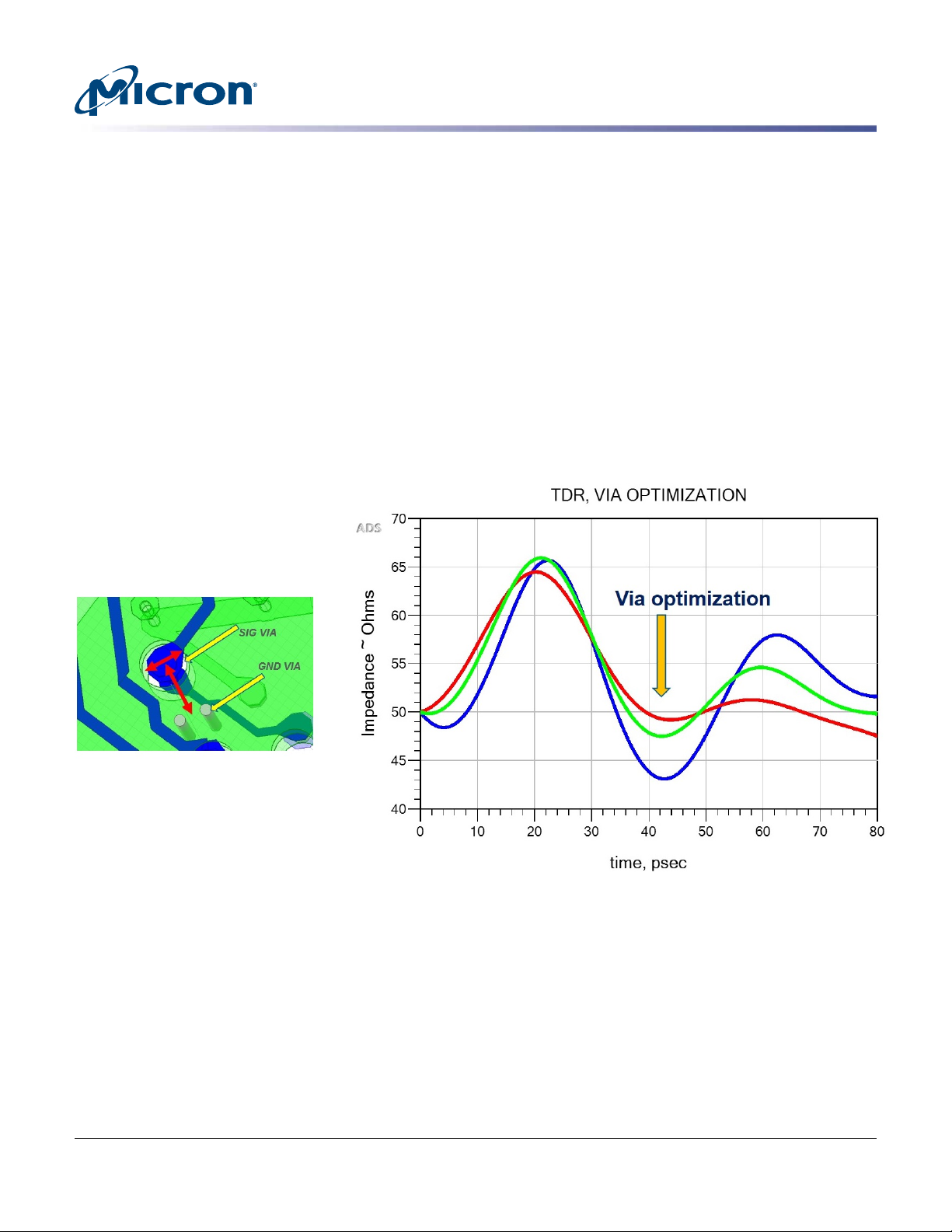
Via Transition Optimization for Return and Insertion Losses
The high-speed signal via transitions need to be optimized to meet the channel target
impedance requirements. The optimization of the via transition should simultaneously
account for the via anti-pad size and the distance between the signal and ground vias in
the immediate vicinity of the transition (as shown in the figure below). Micron recommends a via transition with no more than a -20dB (|S11|<-20dB). For multi-bus transitions, Micron recommends the placement of the ground via to also help mitigate crosstalk, as already discussed in the crosstalk mitigation section.
In the image below, the figure to the right illustrates how the aforementioned variables
(in this case, three anti-pad sizes for a given signal to ground via spacing) can be optimized to make the via transition meet the target impedance (in this case 50 Ohm,
shown in red).
Figure 11: Optimizing Via Transitions
CCM005-524338224-10517
tn_ed_04_gddr6_design_guide.pdf - Rev. B 1/2021 EN
16
Micron Technology, Inc. reserves the right to change products or specifications without notice.
© 2018 Micron Technology, Inc. All rights reserved.
Page 17
TN-ED-04: GDDR6 Design Guide
Layout and Design Considerations
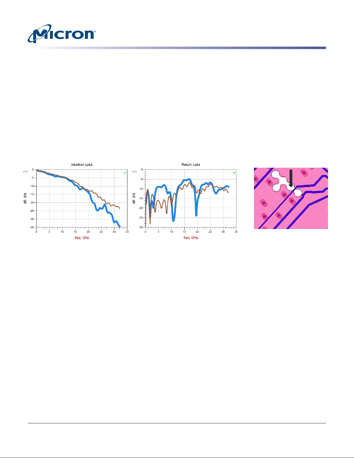
Insertion and Return Loss Improvement: Slot Crossing Elimination
It is important to maintain the minimum possible loop inductance. To help achieve
this, both signal and return path inductances should be kept as low as possible. Slotcrossings (signal crossing a gap in the reference) increase the return path self-inductance and therefore the trace loop inductance, which will have a profound effect on the
insertion loss high frequency response.
In addition, avoiding slot crossings maintains a better impedance balance throughout
the whole span of the trace, improving the return loss. The figures below illustrate the
effect that even a small slot crossing can have on the insertion and return losses. It is
highly recommended that slot crossings are avoided at any cost.
Figure 12: Slot Crossing on Insertion and Return Losses
CCM005-524338224-10517
tn_ed_04_gddr6_design_guide.pdf - Rev. B 1/2021 EN
17
Micron Technology, Inc. reserves the right to change products or specifications without notice.
© 2018 Micron Technology, Inc. All rights reserved.
Page 18

Layout and Design Considerations
Return Loss Improvement: Signal Trace Neckdowns
Sometimes it helps to reduce the width of the signal trace (neckdown) to route it
through via or pin fields. This type of action will change the impedance of the trace and
therefore will affect the overall trace return loss. If a trace transitions through a capacitive discontinuity, necking up to a certain length of the trace adjacent to that discontinuity, might help the return loss in some frequencies.
Necking a trace for long distances, between two sections of nominal impedance, is not
recommended. The length of the necking is a crucial variable in the decision, so careful
consideration is required to meet your return loss specification. The pictures below illustrate the effect of trace necking in the return loss of the signal. Return loss could potentially affect signal-to-noise ratio and the overall performance of the system.
Figure 13: Trace Necking on Return Loss
TN-ED-04: GDDR6 Design Guide
Decision Feedback Equalization
Decision feedback equalization (DFE) can also help overcome degradation in insertion
loss. As an active method, there is an impact to power, and should be considered as further optimization after good board layout has been achieved.
As described in Micron's DesignCon 2019 presentation, Design with Confidence Using
16Gb/s GDDR6 Memory, simulations indicate that benefits of DFE and back drilling are
comparable and additive. Back drilling does tend to address discontinuities beyond the
abilities of DFE. These methods may be used together to maximize signal margin for the
best channel performance.
When using DFE, it is recommended to enable individual per-DQ setting of the DFE coefficient to maximize the DFE ability to reduce ISI. Unless all data traces are identical, a
common DFE coefficient across all DQ pins will over or under equalize the extremes. (In
the simulations performed for the DesignCon paper, this was by as much as 42mV difference.)
CCM005-524338224-10517
tn_ed_04_gddr6_design_guide.pdf - Rev. B 1/2021 EN
18
Micron Technology, Inc. reserves the right to change products or specifications without notice.
© 2018 Micron Technology, Inc. All rights reserved.
Page 19
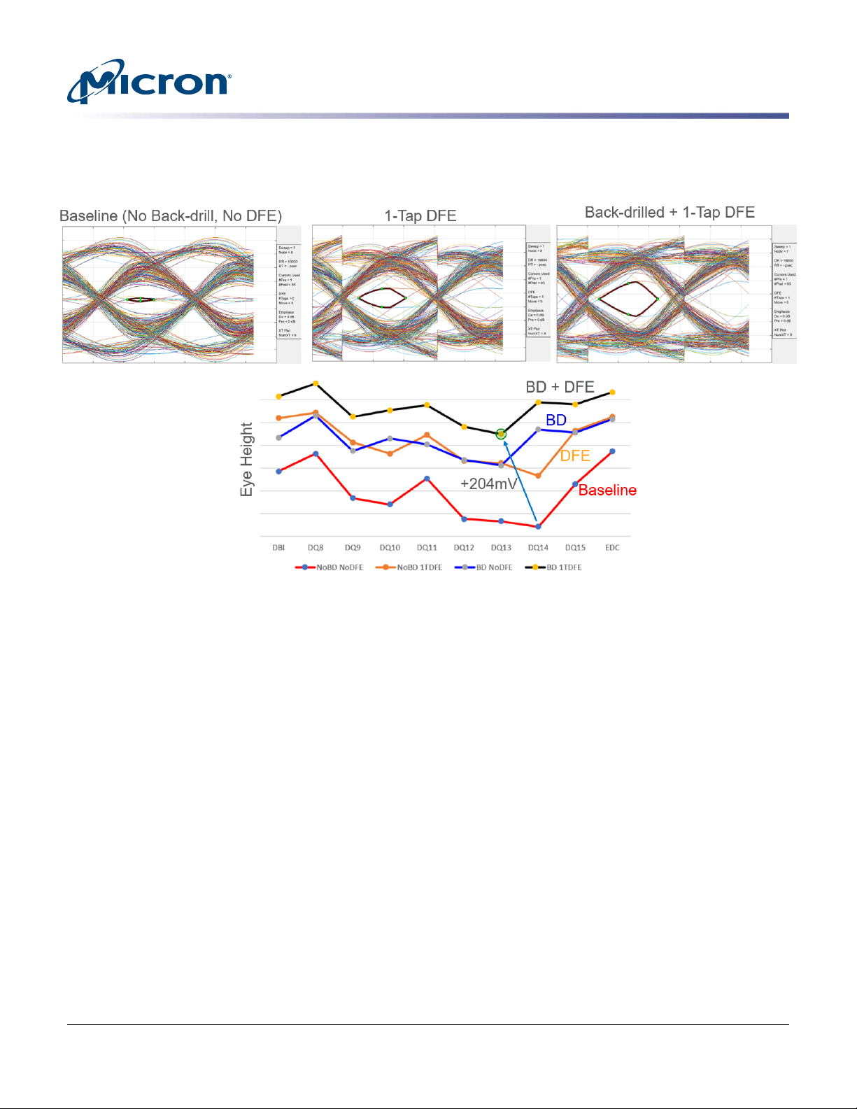
Figure 14: Effect of DFE and Back Drilling
TN-ED-04: GDDR6 Design Guide
Layout and Design Considerations
CCM005-524338224-10517
tn_ed_04_gddr6_design_guide.pdf - Rev. B 1/2021 EN
19
Micron Technology, Inc. reserves the right to change products or specifications without notice.
© 2018 Micron Technology, Inc. All rights reserved.
Page 20

Layout and Design Considerations Summary
• Avoid high-speed signals crossing splits in the power and ground planes.
• Separate supplies and/or flip-chip packaging to help prevent controller SSO occurrence and the strobe/clock collapses it causes.
• Minimize ISI by keeping impedances matched through the channel (traces, via transitions).
• Minimize crosstalk by isolating high-speed and sensitive bits (such as EDC), and
avoiding return-path discontinuities. Isolation can be affected through strategically
inserted ground vias, controlling signal proximity and routing layer.
• Enhance signaling by matching driver impedance with trace impedance.
• Provide ample via stitching between same power and ground domains on different
layers to minimize plane impedance.
• Provide sufficient return vias in proper proximity to power vias to reduce the power
delivery network loop inductance.
• Micron GDDR6N provides drive strength of 60Ω or 48Ω. Micron analysis indicates
good results with a PCB characteristic impedance of approximately 40Ω. This does
depend on the controller as well as DRAM, and care should be taken to match the
channel and driver strengths.
• Properly isolate vias of various power domains.
• Optimize signal transitions to nominal impedance.
TN-ED-04: GDDR6 Design Guide
Layout and Design Considerations
CCM005-524338224-10517
tn_ed_04_gddr6_design_guide.pdf - Rev. B 1/2021 EN
20
Micron Technology, Inc. reserves the right to change products or specifications without notice.
© 2018 Micron Technology, Inc. All rights reserved.
Page 21

Simulations
TN-ED-04: GDDR6 Design Guide
Simulations
For a new or revised design, Micron strongly recommends simulating I/O performance
at regular intervals (pre- and post- layout for example). Optimizing an interface through
simulation can help decrease noise and increase timing margins before building prototypes. Issues are often resolved more easily when found in simulation, as opposed to
those found later that require expensive and time-consuming board redesigns or factory recalls.
Micron has created many types of simulation models to match the different tools in use.
Component simulation models are available. Verifying all simulated conditions is impractical, but there are a few key areas to focus on: DC levels, signal slew rates, undershoot, overshoot, ringing, and waveform shape.
Also, it is extremely important to verify that the design has sufficient signal-eye openings to meet both timing and AC input voltage levels. For additional general information on the simulation process, see the DDR4 SDRAM Point-to-Point Simulation Proc-
ess technical note (TN-46-11) available on micron.com.
CCM005-524338224-10517
tn_ed_04_gddr6_design_guide.pdf - Rev. B 1/2021 EN
21
Micron Technology, Inc. reserves the right to change products or specifications without notice.
© 2018 Micron Technology, Inc. All rights reserved.
Page 22

PCB Stackup
TN-ED-04: GDDR6 Design Guide
Simulations
PCB stackup is an important choice that significantly impacts high-speed signal integrity along with power delivery, noise coupling within the system, and noise emissions/
susceptibility concerns. Selecting an appropriate stackup must carefully balance these
factors, providing a low impedance return path, and allowing for the above high-speed
routing recommendations to be implemented.
As a general guideline, implementing an optimum GDDR6 design in fewer than 8 layers
is not recommended as it makes maintaining good design practices more difficult. The
figure below presents a generic example of an 8-layer stackup that could possibly be
used. This is only one option, as their are many variations in 8 layers or greater that can
readily meet the requirements to implement systems using GDDR6 DRAM.
As described in the above design considerations, key points for the stackup are:
• All high-speed nets should remain on the same reference plane (either power or
ground), all the way from the DRAM pin to the controller pin.
• High speed signals should be routed in stripline; best if both reference layers are VSS/
GND. Having reference to two different reference planes will be sensitive to decoupling. Positioning signal closer to one plane can reduce this sensitivity (see the Recommended Stripline figure below).
• Back-drilling is recommended.
• If back-drilling is available, route high-speed signals in the first stripline environment
nearest to the packaged component (minimize via transition).
• If back-drilling is not available, consider routing in a stripline environment closer to
the opposite side of the board (minimize via stub beyond routing layer in throughhole technology).
• Top-layer microstrip routing may provide a via-free alternative, but should be limited
to very short distances and analyzed carefully for crosstalk and delay implications.
• Perform signal integrity simulation to optimize Clock, WCK, CA, DQ termination and
drive strength, being sure to accurately capture the unique impact of EDC on neighboring signals, and vice versa, for both DRAM READ and WRITE operations.
• Perform simulation to optimize on-board decoupling capacitor placement and values.
• Simplify routing by making use of de-skew functionality of GDDR6 host controller.
• Enabling DFE will increase link margin, providing the best benefit when used with via
stub removal and careful signal routing.
CCM005-524338224-10517
tn_ed_04_gddr6_design_guide.pdf - Rev. B 1/2021 EN
22
Micron Technology, Inc. reserves the right to change products or specifications without notice.
© 2018 Micron Technology, Inc. All rights reserved.
Page 23
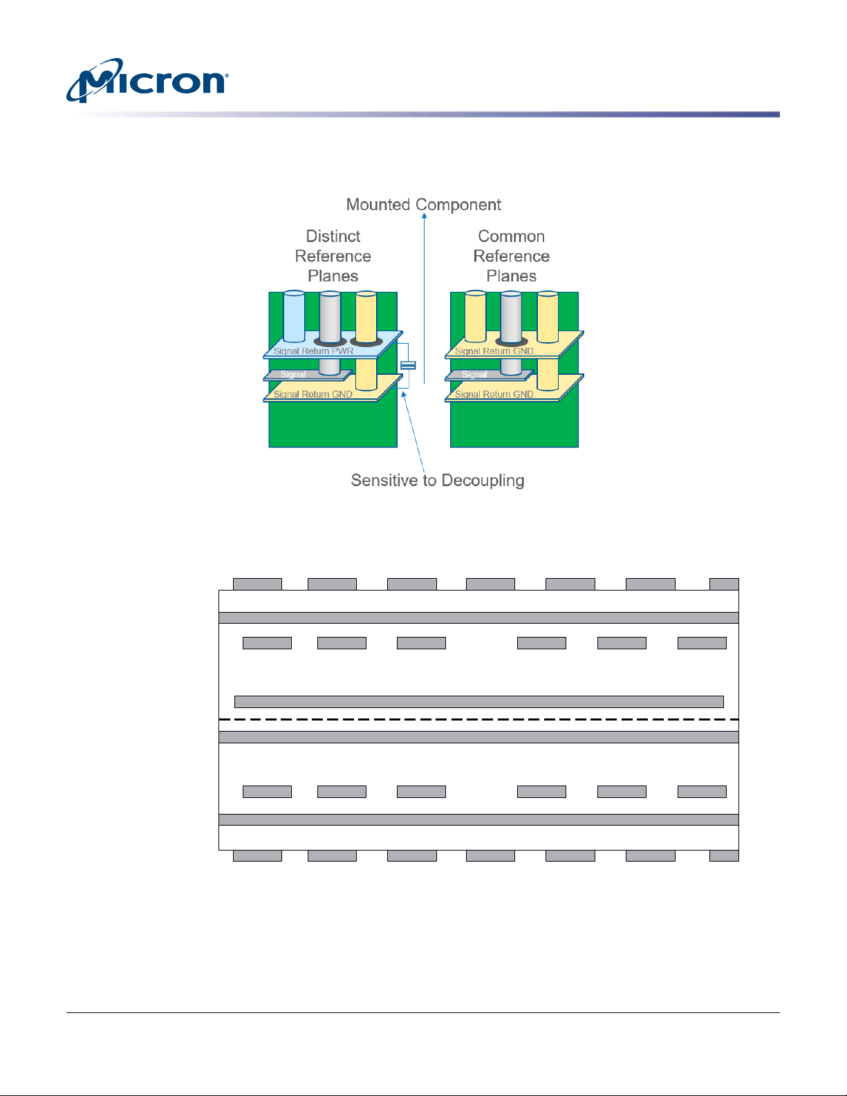
Figure 15: Recommended Stripline
Low speed signal (microstrips)
Low speed signal (microstrips)
1
2
3
4
5
6
7
8
0V plane
Power plane
0V plane
Power plane
Signal (striplines)
Signal (offset striplines)
PCB center line
TN-ED-04: GDDR6 Design Guide
Simulations
Figure 16: PCB Stackup – Example of 8 Layers (4 Signal, 4 Power Planes)
CCM005-524338224-10517
tn_ed_04_gddr6_design_guide.pdf - Rev. B 1/2021 EN
23
Micron Technology, Inc. reserves the right to change products or specifications without notice.
© 2018 Micron Technology, Inc. All rights reserved.
Page 24

References
TN-ED-04: GDDR6 Design Guide
References
• JESD250A Graphics Double Data Rate (GDDR6) SGRAM standard
• Micron GDDR6 SGRAM Technical Note (TN-ED-03)
• Micron 8Gb GDDR6 SGRAM data sheet (available upon request from micron.com)
CCM005-524338224-10517
tn_ed_04_gddr6_design_guide.pdf - Rev. B 1/2021 EN
24
Micron Technology, Inc. reserves the right to change products or specifications without notice.
© 2018 Micron Technology, Inc. All rights reserved.
Page 25

Revision History
Rev. B – 1/21
Rev. A – 7/18
TN-ED-04: GDDR6 Design Guide
Revision History
• Updated Figure 1, Figure 5
• Updated High Speed Via Isolation to Mitigate Crosstalk section, Layout and Design
Considerations section, and PCB Stackup section
• Added Decision Feedback Equalization section
• Initial release
CCM005-524338224-10517
tn_ed_04_gddr6_design_guide.pdf - Rev. B 1/2021 EN
8000 S. Federal Way, P.O. Box 6, Boise, ID 83707-0006, Tel: 208-368-4000
www.micron.com/products/support Sales inquiries: 800-932-4992
Micron and the Micron logo are trademarks of Micron Technology, Inc.
All other trademarks are the property of their respective owners.
25
Micron Technology, Inc. reserves the right to change products or specifications without notice.
© 2018 Micron Technology, Inc. All rights reserved.
 Loading...