


WT32i BLUETOOTH AUDIO MODULE
PRELIMINARY DATA SHEET
Monday, 11 November 2013
Version 0.2

Copyright © 2000-2013 Bluegiga Technologies
All rights reserved.
Bluegiga Technologies assumes no responsibility for any errors which may appear in this manual.
Furthermore, Bluegiga Technologies reserves the right to alter the hardware, software, and/or specifications
detailed here at any time without notice and does not make any commitment to update the information
contained here. Bluegiga’s products are not authorized for use as critical components in life support devices
or systems.
The WRAP is a registered trademark of Bluegiga Technologies
The Bluetooth trademark is owned by the Bluetooth SIG Inc., USA and is licensed to Bluegiga Technologies.
All other trademarks listed herein are owned by their respective owners.
Bluegiga Technologies Oy

VERSION HISTORY
VERSION
COMMENT
0.1
Draft
0.2
Updated product codes and contact info
Bluegiga Technologies Oy

TABLE OF CONTENTS
1 WT32i Product Numbering ........................................................................................................................... 7
2 Block diagram ............................................................................................................................................... 8
3 Pinout and Terminal Description .................................................................................................................. 9
4 Electrical Characteristics ............................................................................................................................ 12
4.1 Absolute Maximum Ratings ................................................................................................................ 12
4.2 Recommended Operating Conditions ................................................................................................. 12
4.3 Digital Terminals.................................................................................................................................. 12
4.4 Audio Characteristics .......................................................................................................................... 13
4.4.1 ADC .............................................................................................................................................. 13
4.4.2 DAC .............................................................................................................................................. 13
4.4.3 A2DP Codecs............................................................................................................................... 14
4.5 RF Characteristics ............................................................................................................................... 16
4.5.1 RF Transceiver ............................................................................................................................ 16
4.5.2 Antenna Characteristics ............................................................................................................... 17
4.6 Current Consumption .......................................................................................................................... 20
5 Power Control and Regulation ................................................................................................................... 21
5.1 Reset ................................................................................................................................................... 23
5.1.1 Internal POR ................................................................................................................................ 24
6 Battery Charger .......................................................................................................................................... 26
7 GPIO and AIO Functions ............................................................................................................................ 27
7.1 iWRAP supported GPIO Functions ..................................................................................................... 27
7.2 Wi-Fi Co-existence Signals ................................................................................................................. 27
7.3 Outputting Internal Clocks ................................................................................................................... 29
7.4 Auxiliary ADC ...................................................................................................................................... 29
7.5 Software I2C Interface ........................................................................................................................ 29
8 Serial Interfaces .......................................................................................................................................... 30
8.1 UART Interface .................................................................................................................................... 30
8.1.1 Resetting Through UART Break Signal ....................................................................................... 31
8.1.2 UART Configuration While Reset is Active .................................................................................. 31
8.1.3 UART Bypass Mode .................................................................................................................... 31
8.2 USB Interface ...................................................................................................................................... 31
8.3 Programming and Debug Interface (SPI) ............................................................................................ 33
9 Audio Interfaces .......................................................................................................................................... 34
9.1 Stereo Audio Codec Interface ............................................................................................................. 34
9.1.1 ADC .............................................................................................................................................. 34
9.1.2 DAC .............................................................................................................................................. 36
9.1.3 Microphone Input ......................................................................................................................... 37
Bluegiga Technologies Oy

9.1.4 Line Input ..................................................................................................................................... 38
9.1.5 Output Stage ................................................................................................................................ 39
9.1.6 Mono Operation ........................................................................................................................... 41
9.1.7 Side Tone ..................................................................................................................................... 41
9.2 PCM Interface ..................................................................................................................................... 41
9.3 I2S Interface ........................................................................................................................................ 41
9.4 IEC 60958 Interface ............................................................................................................................ 43
10 Design Guidelines ................................................................................................................................... 45
10.1 Audio Layout Guide ..................................................................................................................... 45
10.1.1 EMC Considerations .................................................................................................................... 45
10.1.2 Choosing Capacitors and Resistors ............................................................................................ 45
10.2 RF Layout Guide .......................................................................................................................... 46
10.3 Example Application Schematics ................................................................................................. 49
11 Physical Dimensions ............................................................................................................................... 53
12 Soldering Recommendations .................................................................................................................. 55
13 Package .................................................................................................................................................. 56
14 Certification Guidance for an End Product Using WT32i........................................................................ 58
14.1 Bluetooth End Product Listing ...................................................................................................... 58
14.2 CE Approval of an End-Product ................................................................................................... 58
14.3 FCC Certification of an End Product ............................................................................................ 59
14.3.1 Co-location with Other Transmitters ............................................................................................ 60
14.4 IC Certification of an End Product ............................................................................................... 60
14.5 MIC Japan Certification of an End Product .................................................................................. 60
15 WT32i Certifications ................................................................................................................................ 60
15.1 Bluetooth ...................................................................................................................................... 60
15.2 CE ................................................................................................................................................ 60
15.3 FCC .............................................................................................................................................. 61
15.4 IC .................................................................................................................................................. 62
15.4.1 IC .................................................................................................................................................. 62
15.5 MIC Japan .................................................................................................................................... 63
15.6 KCC (South Korea) ...................................................................................................................... 63
15.7 Qualified Antenna Types for WT32i-E ......................................................................................... 63
16 Contact Information................................................................................................................................. 64
Bluegiga Technologies Oy

WT32i Bluetooth® Audio Module
DESCRIPTION
WT32i is the latest generation of Bluetooth
modules. It provides highest level of
integration with integrated 2.4GHz radio, DSP,
battery charger, stereo codec, and antenna
ready to hit mono and stereo audio
applications. WT32i is also ready to support
the latest Bluetooth 3.0 standard.
The embedded DSP core allows enhancement
of the product with features such as advanced
audio decoding (MP3, AAC, AAC+, aptX®),
echo cancellation, noise reduction, and data
manipulation.
Bluegiga’s flexible iWRAP firmware enables
device manufacturers to easily add wireless,
secure, and standard-based Bluetooth
connectivity into new or existing applications
with very limited development and
manufacturing effort.
WT32i is qualified as a Bluetooth Controller
Subsystem. Combining with iWRAP Host
Subsystem it makes a complete Bluetooth End
Product without any additional Bluetooth
qualifications. WT32i has FCC, IC, MIC Japan
and KCC modular certification and it is fully
tested for CE minimizing the certification costs
for the end product.
KEY FEATURES:
Plug n’ Play Bluetooth Solution for
Mono and Stereo Audio Solutions
Integrated DSP, Stereo Codec, and
Battery Charger
Integrated Antenna and W.FL
Connector
Bluetooth 3.0 Compliant
Bluetooth, CE, FCC, IC, KCC and MIC
Japan Qualified
Class 1 - Range up to 100 Meters
Temperature range from
-40C to +85C
Low Power Consumption
iWRAP™ Firmware for Controlling
Connections and Configuring Settings
Supported Bluetooth Profiles: A2DP,
AVRCP, HFP, HFP-AG, SPP, OPP, FTP,
HSP, DUN, PBAP and HID
APPLICATIONS:
High quality wireless stereo headsets
Wireless speakers
Hands-free car kits
Bluegiga Technologies Oy

1 WT32i Product Numbering
WT32i-A-AI
Product series
Fimrware
AI5 = iWRAP 5.0.2
C = custom
HW version
A = Chip antenna, industrial temperature
range
E = W.FL connector, industrial
temperature range
Bluegiga Technologies Oy
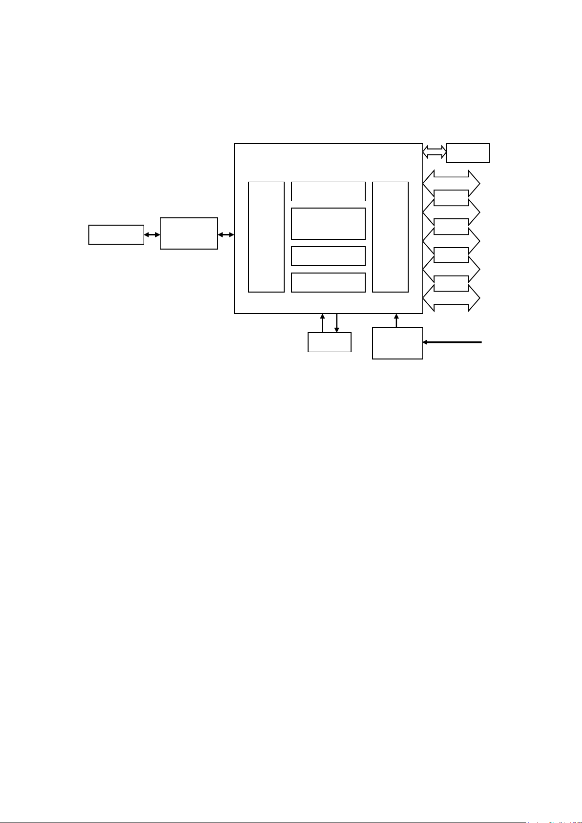
2 Block diagram
RAM
Baseband
DSP
MCU
Kalimba DSP
2.4
GHz
Radio
I/O
BC05-MM
XTAL
Balanced
filtter
Antenna
Flash
UART/USB
PIO
Audio In/Out
PCM/I2S
SPI
Reset
circuitry
Figure 1: Block Diagram of WT32i
BC05-MM
The BlueCore®5-Multimedia External is a single-chip radio and baseband IC for Bluetooth 2.4GHz systems. It
provides a fully compliant Bluetooth v3.0 specification system for data and voice. BlueCore5-Multimedia
External contains the Kalimba DSP coprocessor with double the MIPS of BlueCore3-Multimedia External,
supporting enhanced audio applications.
XTAL
Ther reference clock of WT32i is generated with 26 MHz crystal. All BC05-MM internal digital clocks are
generated using a phase locked loop, which is locked to the frequency of either the 26 MHz crystal or an
internally generated watchdog clock frequency of 1kHz.
RESET CIRCUITRY
The internal reset circuitry keeps BC05-MM in reset during boot in order for the supply voltages to stabilize.
This is to prevent corruption of the flash memory during booting. Please see chapter 5.1 for more detailed
description.
BALANCED FILTER
The internal balanced filter provides optimal impedance matching and band pass filtering in order to achieve
lowest possible in-band and out-of-band emissions.
ANTENNA
The antenna is a ceramic chip antenna with high efficiency. The antenna is insensitive to surrounding
dielectric materials and requires only a small clearance underneath which makes it compatible with previous
WT32I designs and well suitable for designs with high density.
FLASH
16 Mbit flash memory is used for storing the Bluetooth protocol stack and Virtual Machine applications. It can
also be used as an optional external RAM for memory-intensive applications.
Bluegiga Technologies Oy
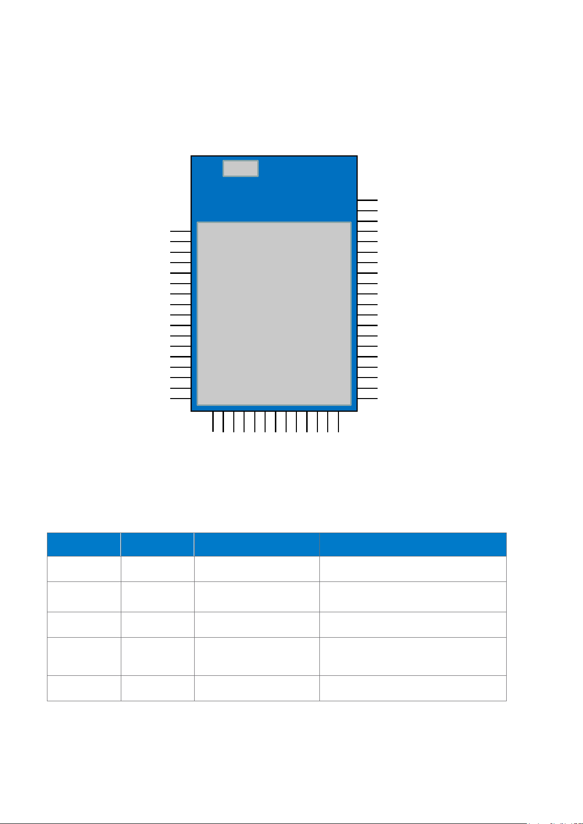
AUDIO_OUT_N_LEFT
AUDIO_OUT_P_LEFT
AUDIO_OUT_P_RIGHT
AUDIO_OUT_N_RIGHT
GND
AUDIO_IN_N_LEFT
AUDIO_IN_P_LEFT
GND
AUDIO_IN_N_RIGHT
AUDIO_IN_P_RIGHT
MIC_BIAS
GND
VDD_CHG
VDD_BAT
LED0
SPI_MOSI
SPI_MISO
SPI_CLK
SPI_NCSB
PCM_CLK
PCM_SYNC
PCM_OUT
PCM_IN
PIO4
PIO5
PIO6
PIO7
PIO8
UART_NCTS
UART_NRTS
RESET
GND
VDD_IO
UART_TXD
UART_RXD
PIO10
PIO9
USB_D+
USB_D-
PIO3
PIO2
PIO1
PIO0
AIO1
AIO0
GND
GND
GND
VREG_ENA
1
2
3
4
5
6
7
8
9
10
11
12
13
14
15
16
17
GND
47
46
45
44
43
42
41
40
39
38
37
36
35
34
33
32
31
50
49
48
18
19202122232425
26
272829
30
Pin Number
Pin Name
Pad Type
Description
1
VREG_ENA
Input
SW configurable enable pin for the
internal regulators
2-3, 18, 31,
39, 43, 48
GND
GND
GND
17
VDD_IO
Power supply
1.7V - 3.6V power supply for the serial
interfaces and GPIOs
37
VDD_BAT
Power supply / Charger
output
2.7V - 4.4V supply voltage for the
internal regulators and output of the
battery charger
38
VDD_CHG
Power supply
Nominal 5V supply voltage for the
battery charger
3 Pinout and Terminal Description
Figure 2: WT32i
Table 1: Supply Terminal Descriptions
Bluegiga Technologies Oy
Page 9 of 64

Pin
Number
Pin Name
Pin Type
Description
19
RESET
RESET
Active high reset. If not used, leave floating. When
connected, make sure that the reset is either pulled
high or floating (connected to high impedance)
during boot.
5
AIO0
Configurable I/O
AIO0 and AIO1 can be used to read the voltage
level through the internal ADC (refer to iWRAP
User Guide for details). AIO pins can also be
configured to be used as general digital IO pins
through PS settings. Internal clocks can be routed
out through AIO pins by setting corresponding PS
settings. Note that the AIO pins are powered from
internal 1.5V supply so the maximum voltage level
of the AIO pins is 1.5V.
6
AIO1
7
PIO0
Configurable CMOS I/O
General purpose IO's can be configured with
iWRAP for various functions. Each IO can be
configured individually as output or input with
strong or weak pull-up/-down. Using particular PS
setting GPIO pins can be used to implement WiFi
co-existence signaling between WT32i and a WiFi
radio. Software I2C interface can be implemented
for slow I2C functions such as configuring external
audio codec or display.
8
PIO1
9
PIO2
10
PIO3
13
PIO9
14
PIO10
22
PIO8
23
PIO7
24
PIO6
25
PIO5
26
PIO4
11
USB_D-
I/O
USB data minus
12
USB_D+
I/O
USB data plus with selectable internal 1.5k pull-up
resistor
15
UART_RXD
CMOS Input, weak internal
pull-down
UART data input
16
UART_TXD
CMOS output, tristate,
weak internal pull-up
UART data output
20
UART_NRTS
CMOS output, tristate,
weak internal pull-up
UART request to send, active low
21
UART_NCTS
CMOS Input, weak internal
pull-down
UART clear to send, active low
32
SPI_NCSB
CMOS Input, weak internal
pull-down
SPI chip select
33
SPI_CLK
CMOS Input, weak internal
pull-down
SPI clock
Bluegiga Technologies Oy
Page 10 of 64
34
SPI_MISO
CMOS Input, weak internal
pull-down
SPI data input
35
SPI_MOSI
CMOS output, tristate,
weak internal pull-down
SPI data output
36
LED0
Open drain output
LED driver
Pin
Number
Pin Name
Pin Type
Description
40
MIC_BIAS
Analog
41
AUDIO_IN_P_RIGHT
Analog
42
AUDIO_IN_N_RIGHT
Analog
44
AUDIO_IN_P_LEFT
Analog
45
AUDIO_IN_N_LEFT
Analog
46
AUDIO_OUT_N_RIGHT
Analog
47
AUDIO_OUT_P_RIGHT
Analog
49
AUDIO_OUT_N_LEFT
Analog
50
AUDIO_OUT_P_LEFT
Analog
26
PCM_IN / I2S IN
CMOS input, weak
internal pull-down
PCM or I2S data input
27
PCM_OUT / I2S_OUT
CMOS outptu, tristate,
weak internal pull-down
PCM or I2S data output
28
PCM_SYNC / I2S_WS
Bidirectional, weak
internal down
PCM sync or I2S word select. WT32i can
operate as a PCM/I2S master providing the
sync or as a slave receiving the sync
29
PCM_CLK / I2S_SCK
Bidirectional, weak
internal down
PCM or I2S clock. WT32i can operate as a
PCM/I2S master providing the clock or as
a PCM slave receiving the PCM clock. I2S
slave mode is not supported
Table 2: Terminal Descriptions
Table 3: Audio Terminal Descriptions
Bluegiga Technologies Oy
Page 11 of 64
Min
Max
Unit
Storage temperature range
-40
+85
°C
Operating temperature range
-40
+85
°C
VDD_IO
-0.4
3.6
V
VDD_BAT
-0.4
4.4
V
VDD_CHG
-0.4
6.5 V Digital Terminal voltages
VSS - 0.4V
VDD + 0.4V
V
AIO voltages
VSS - 0.4V
1.9V
V
Min
Max
Unit
Storage temperature range
-40
+85
°C
Operating temperature range
-40
+85
°C
VDD_IO
1.7
3.6
V
VDD_BAT
2.7
4.4
V
VDD_CHG
0
6.5
V
Digital Terminal voltages
0
VDD
V
AIO voltages
0
1.5V
V
Input/Output Characteristic
Min
Max
Unit
V
IL
input logic level low
-0.3
0.25 x VDD
V
V
IL
input logic level high
0.625 x VDD
VDD + 0.3
V
V
OL
output logic level low, I
OL
= 4.0mA
0
0.125
V
V
OL
output logic level high, I
OL
= -4.0mA
0.75 x VDD
VDD
V
Strong pull-up
-100
-10
µA
Strong pull-down
10
100
µA
Weak pull-up
-5
-0.2
µA
Weak pull-down
0.2
5
µA
4 Electrical Characteristics
4.1 Absolute Maximum Ratings
Table 4: Absolute Maximum Ratings
4.2 Recommended Operating Conditions
Table 5: Recommended operating conditions
4.3 Digital Terminals
Table 6: Digital Terminal Characteristics
Bluegiga Technologies Oy
Page 12 of 64
4.4 Audio Characteristics
Parameter
Conditions
Min
Typ
Max
Unit
Resolution
-
-
-
16
Bits
Input Sample
Rate, F
sample
-
8 - 44.1
kHz
Signal to Noise
Ratio, SNR
F
sample
8kHz
-
79 - dB
11.025kHz
-
77 - dB
16kHz
-
76 - dB
22.050kHz
-
76 - dB
32kHz
-
75 - dB
44.1kHz
-
75 - dB
Input full scale at maximum gain (differential)
-
4
-
mV rms
Input full scale at minimum gain (differential)
-
800
-
mV rms
3dB Bandwidth
-
20 - kHz
Microphone mode input impedance
-
6.0 - kHz
THD+N @ 30mV rms input
-
0.04 - %
Parameter
Conditions
Min
Typ
Max
Unit
Resolution
-
-
-
16
Bits
Output Sample
Rate, F
sample
-
8
-
48
kHz
Signal to Noise
Ratio, SNR
F
sample
8kHz
-
95 - dB
11.025kHz
-
95 - dB
16kHz
-
95 - dB
22.050kHz
-
95 - dB
32kHz
-
95 - dB
44.1kHz
-
95 - dB
Output Full Voltage Swing (differential)
-
750
-
mV rms
Allowed Load
Resistive
16 - O.C.
Ω
Capacitive
-
-
500
pF
4.4.1 ADC
4.4.2 DAC
Table 7: ADC characteristics
Bluegiga Technologies Oy
Page 13 of 64
THD+N 16Ω Load
-
-
0.1 % THD+N 100Ω Load
-
-
0.01
%
Table 8: DAC Characteristics
4.4.3 A2DP Codecs
4.4.3.1 SBC
SBC codec is the default codec used for Bluetooth A2DP connections. Any Bluetooth device supporting A2DP
audio profile supports SBC codec. SBC was originally design to provide reasonable good audio quality while
keeping low computational complexity. SBC does not require high bit rates. Thus it works sufficiently with
Bluetooth where the bandwidth and the processing power are limited.
4.4.3.2 aptX®
The aptX is widely used in high quality audio devices. aptX can provide dynamic range up to 120 dB and it
has the shortest coding delay (<2ms) than other coding algorithms. Using aptX® the whole system latency can
be reduced significantly because unlike SBC, it does not require buffering the audio. SBC reproduces a limited
audio band width whereas aptX® encode the entire frequency range of audio.
aptX® is more robust and resilient coding scheme than SBC and thus re-transmits does not occur as with
SBC.
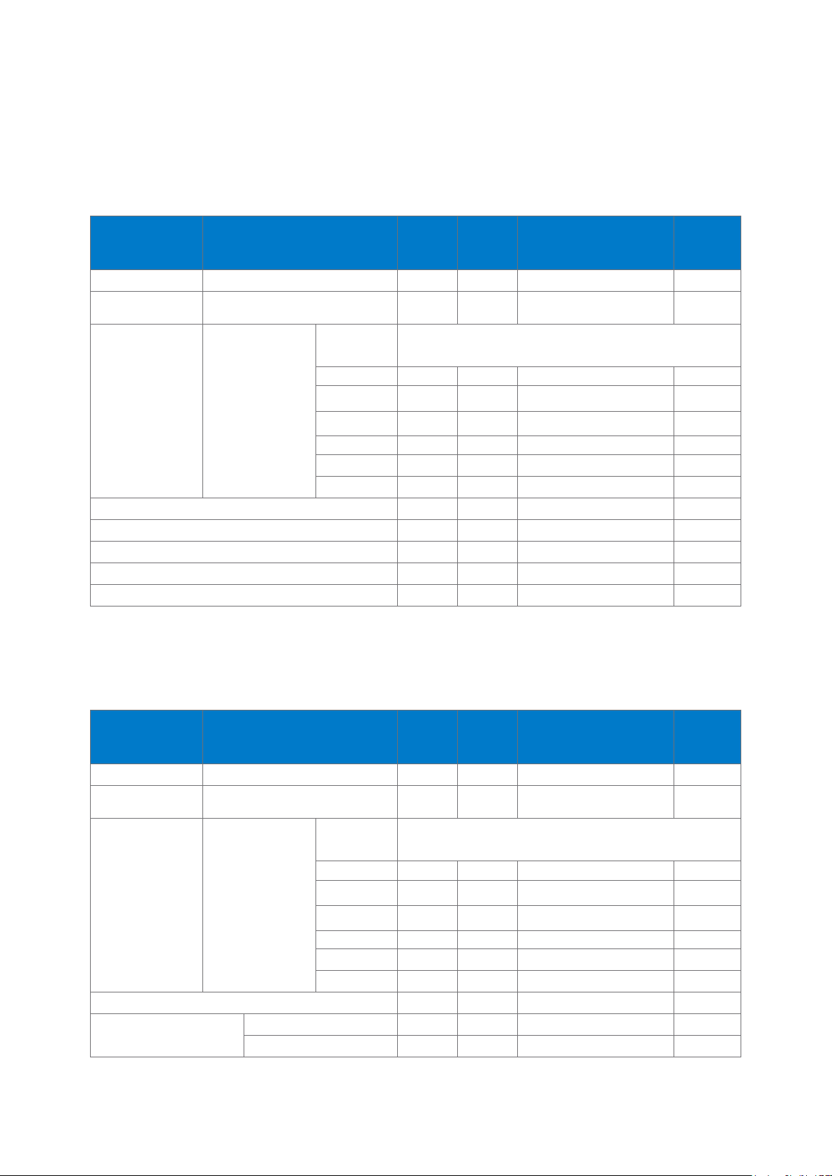
Both SBC and aptX® have flat frequency response up to 14 kHz. Up to 14 kHz both algorithms produce good
quality audio with very little distortion. At frequencies higher than 14 kHz the benefit of aptX® becomes
obvious. SBC exhibits increasing attenuation with increasing frequency but aptX® retains high reproduction
quality.
aptX®requires purchasing a license for each Bluetooth address and the license agreement must be done with
CSR. The combination of aptX® license and the Bluetooth address is programmed into the module in the
module production line.
Figure 3: Frequency response of aptX and SBC codecs
Bluegiga Technologies Oy
Page 14 of 64

4.4.3.3 AAC
AAC (Advanced Audio Coding) achieves better sound quality than MP3 and it is the default audio format for
YouTube and iPhone among others. AAC has long latency (>100ms) compared to aptX®. Because of high
processing capacity requirement for encoding, WT32i does not support AAC as A2DP source. Thus WT32i
can be used for receiving (A2DP sink) AAC (from iPhone for example) but it can not transmit AAC coded
audio.
Bluegiga Technologies Oy
Page 15 of 64
4.5 RF Characteristics
Transceiver characteristic
Min
Typ
Max
Unit
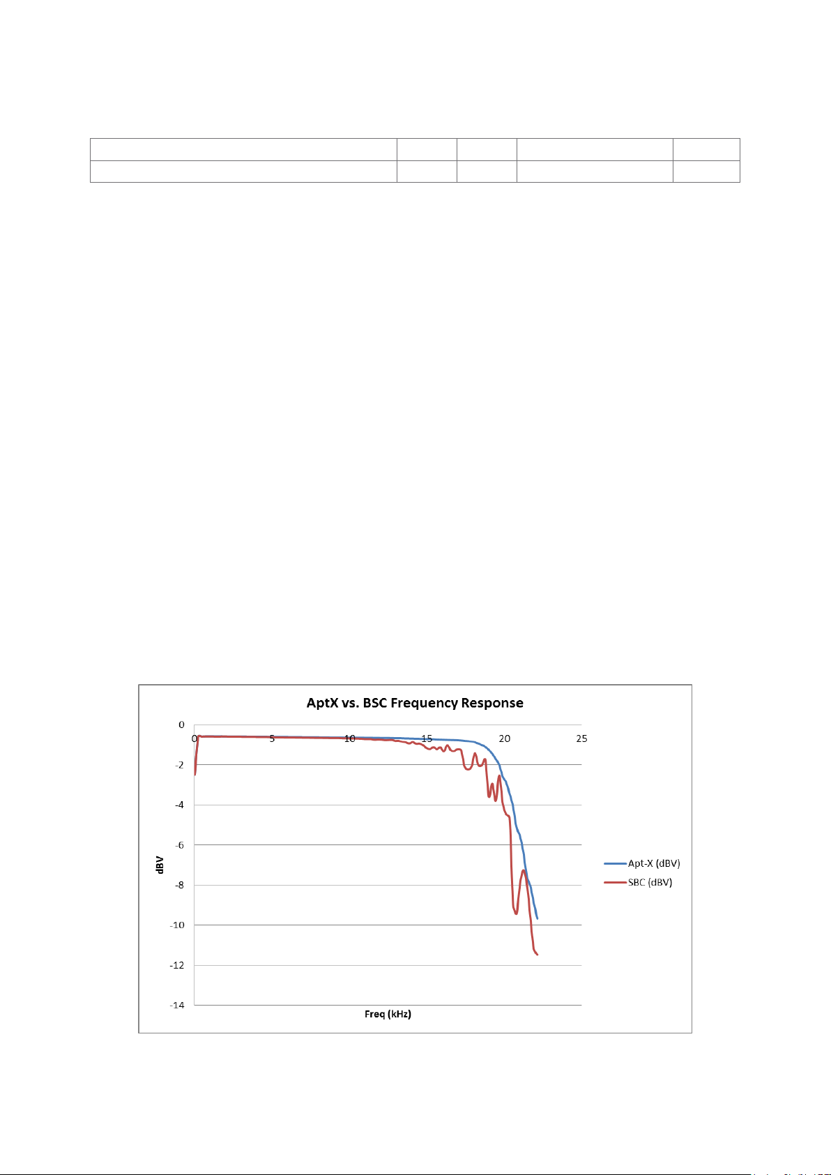
Maximum transmit power
4.5
6
7.5
dBm
Minimum transmit power
-17
dBm
Transmit power stability over the temperature range
+/- 0.5
dB
Transmit power variation within the BT band
1
dB
Sensitivity DH1
RT
-90
dBm
-40C
-91
dBm
+85C
-86
dBm
Sensitivity 3DH5
RT
-83
dBm
-40C
-84
dBm
+85C
-80
dBm
4.5.1 RF Transceiver
Table 9: Transceiver characteristics
Table 10: Power control of WT32i
Bluegiga Technologies Oy
Page 16 of 64

Standard
Band /
Frequency
Min
(AVG /
PEAK)
Typ
(AVG /
PEAK)
Max
(AVG /
PEAK)
Limit by the Standard
(AVG / PEAK)
Unit
FCC part 15
transmitter
spurious
emissions
2nd harmonic
50 / 61
54 / 74
dBuV/m
3rd harmonic
< 40 /
50
54 / 74
dBuV/m
Band edge
2390MHz
54 / 74
dBuV/m
Band edge
2483.5MHz
54 / 74
dBuV/m
Band edge
2400MHz
(conducted)
-20
dBc
Band edge
2483.5MHz
(conducted)
-20
dBc
ETSI EN 300
328 transmitter
spurious
emissions
Band edge
2400MHz
-30
dBm
2nd harmonic
-35
-30
dBm
3rd harmonic
<-40
-30
dBm
ETSI EN 300
328 receiver
spurious
emissions
(2400 - 2479)
MHz
-47
dBm
(1600 - 1653)
MHz
-47
dBm
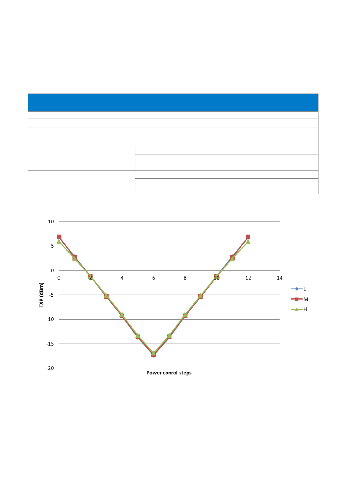
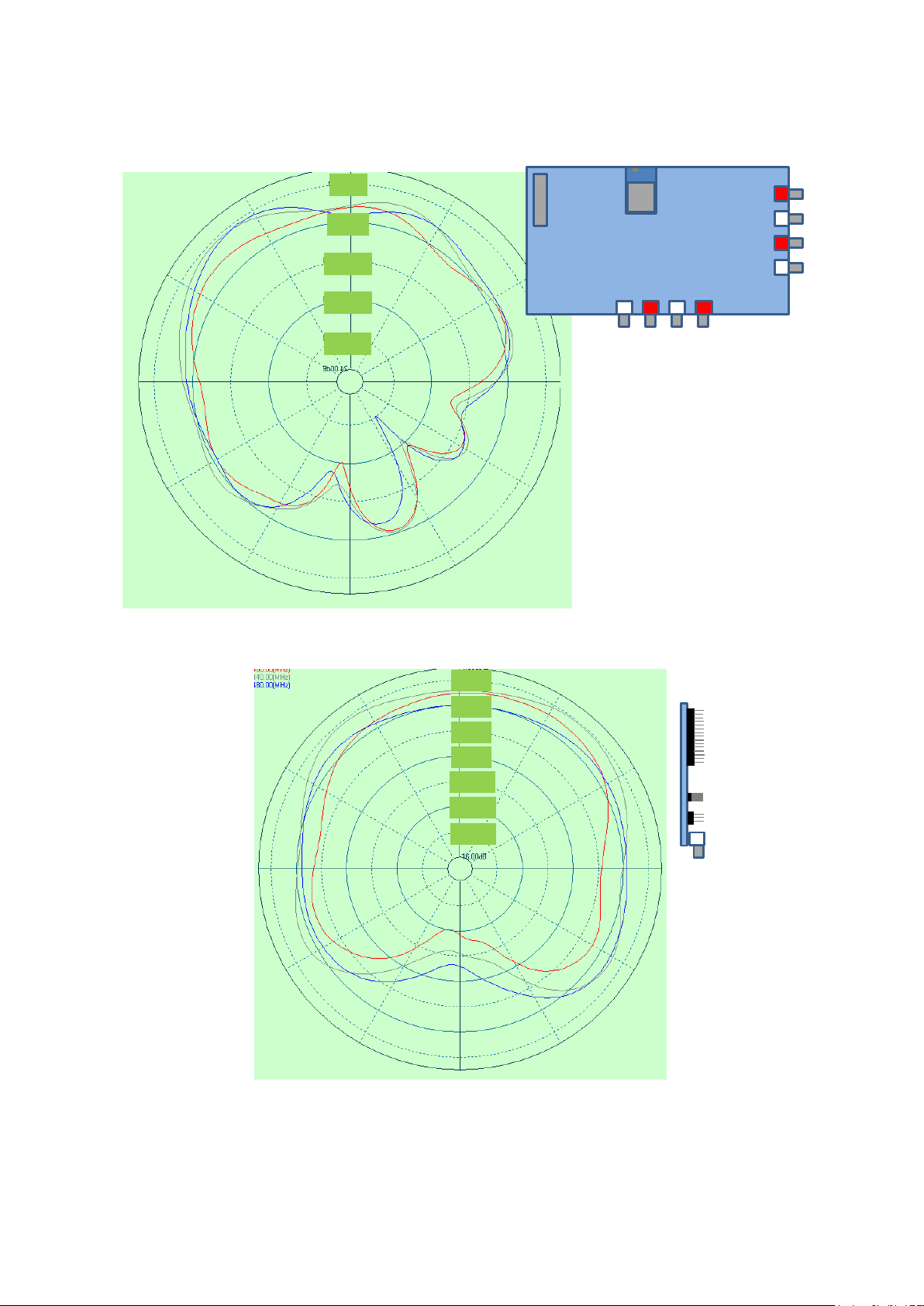
4.5.2 Antenna Characteristics
Note: Antenna characteristics may vary depending on the mother board layout. Following characteristics have
been measured using DKWT32i
Antenna efficiency -3.5 dB (45%)
Peak gain 0 dBi
All the emissions tested with maximum 8 dBm TX power
Table 11: WT32i-A spurious emissions
Bluegiga Technologies Oy
Page 17 of 64
0 dB
-5 dB
-10 dB
-15 dB
-20 dB
-2 dB
-4 dB
-6 dB
-8 dB
-10 dB
-12 dB
-14 dB
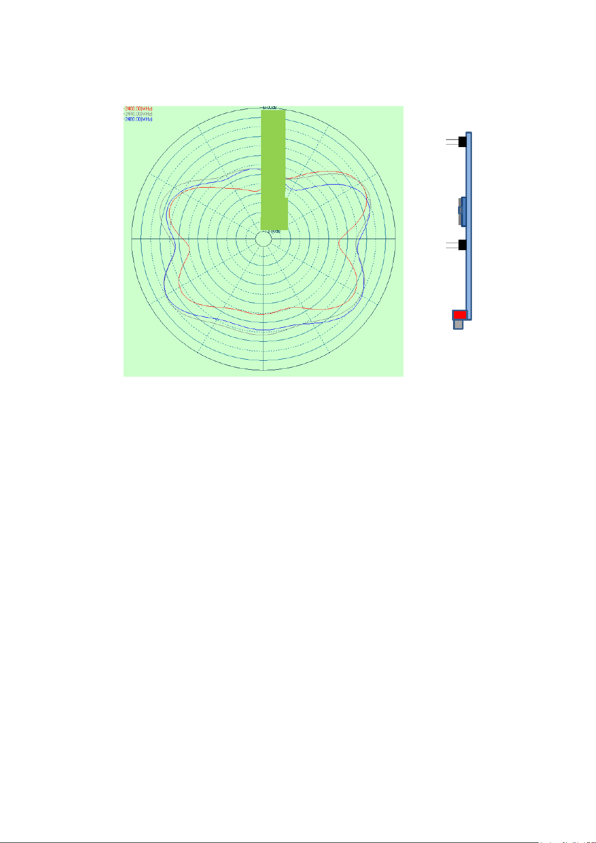
Figure 4: Top view radiation pattern of DKWT32i
Figure 5: Side view radiation pattern of DKWT32i
Bluegiga Technologies Oy
Page 18 of 64
-1 dB
-2 dB
-3 dB
-4 dB
-5 dB
-6 dB
-7 dB
-8 dB
-9 dB
-10 dB
-11 dB
-12 dB
Figure 6: Front view radiation pattern
Bluegiga Technologies Oy
Page 19 of 64

4.6 Current Consumption
Operation Mode
Peak
Average
Unit
Idle
SET BT PAGEMODE 0 2000 0
12
2.0
mA
SET BT PAGEMODE 0 2000 1
2.0
SET BT PAGEMODE 0 2000 2
2.0
SET BT PAGEMODE 1 2000 0
32
2.0
SET BT PAGEMODE 1 2000 1
2.1
SET BT PAGEMODE 1 2000 2
2.1
SET BT PAGEMODE 2 2000 0
23
SET BT PAGEMODE 2 2000 1
2.2
SET BT PAGEMODE 2 2000 2
2.1
SET BT PAGEMODE 3 2000 0
23
SET BT PAGEMODE 3 2000 1
2.3
SET BT PAGEMODE 3 2000 2
2.2
SET BT PAGEMODE 4 2000 0
23
SET BT PAGEMODE 4 2000 1
2.3
SET BT PAGEMODE 4 2000 2
2.2
Sleep
SET BT PAGEMODE 0 2000 0
12
0.08
mA
SET BT PAGEMODE 0 2000 1
0.08
SET BT PAGEMODE 0 2000 2
0.08
SET BT PAGEMODE 1 2000 0
32
0.18
SET BT PAGEMODE 1 2000 1
0.18
SET BT PAGEMODE 1 2000 2
0.18
SET BT PAGEMODE 2 2000 0
23.5
SET BT PAGEMODE 2 2000 1
0.31
SET BT PAGEMODE 2 2000 2
0.19
SET BT PAGEMODE 3 2000 0
23
SET BT PAGEMODE 3 2000 1
0.4
SET BT PAGEMODE 3 2000 2
0.29
SET BT PAGEMODE 4 2000 0
23
SET BT PAGEMODE 4 2000 1
0.4
SET BT PAGEMODE 4 2000 2
0.29
Connected, Sniff disabled
SET BT SNIFF 0 20 1 8
4.7
Connected + Sniff, Master
SET BT SNIFF 40 20 1 8
3.9
Connected + Sniff, Master
SET BT SNIFF 1000 20 1 8
2.5
Connected + Sniff, Slave
SET BT SNIFF 40 20 1 8
3.6
Connected + Sniff, Slave
SET BT SNIFF 1000 20 1 8
2.5
A2DP Audio Streaming
A2DP SINK, INTERNAL CODEC
75
28
mA
A2DP Audio Streaming
A2DP SOURCE, INTERNAL CODEC
70
23
Table 12: Current consumption of WT32i
Bluegiga Technologies Oy
Page 20 of 64

Battery Charger
In
Out
Switch mode
1.8V regulator
Linear 1.5V
regulator
AIO
RF
Core
Audio
Flash
PIO
USB
UART
PCM
VDD_CHG
VDD_BAT
VREG_ENA
VDD_IO
5 Power Control and Regulation
WT32i contains an internal battery charger and a switch mode regulator that is mainly used for internal blocks
of the module. The module can be powered from a single 3.3 V supply provided that VDD_CHG is floating.
Alternatively the module can be powered from a battery connected to VDD_BAT and using an external
regulator for VDD_IO. 1.8 V to 3.3 V supply voltage for VDD_IO can be used to give desired signal levels for
the digital interfaces of the module. USB, however, requires 3.3 V for proper operation and thus, when USB is
in use, 3.3 V for VDD_IO is required.
Figure 7: Power supply configuration of WT32i
VDD_ENA is software configurable enable pin for the internal regulators. Using iWRAP the enable pin can be
configured to
1. Latch on the internal regulators at the rising edge
2. Turn the regulators on at rising edge and turn off the regulators at falling edge
3. Latch the regulators on at the rising edge and turn off the regulators at the following rising edge
GPIO can be configured to control an external regulator.
Bluegiga Technologies Oy
Page 21 of 64

R1
R2
LDO
(1.8V...3.6V)
EN
IN
VDD_BAT
VREG_ENA
VDD_IO
GPIO (holds the external LDO on)
ON/OFF
Button
Battery Voltage
(2.7V...4.4V)
C1
100k
100k
4u7
Figure 8: Example of making a power on/off button using the latch feature of the internal regulators
iWRAP Example: Creating an on/off button with PIO2 holding the external regulator on
“SET CONTROL VREGEN 2 4”
(PIO is defined with a bit mask. 4 in hexadecimal is 100 in binary corresponding to PIO2)
NOTE: With the configuration shown above, when doing a SW reset for the module C1 will hold the enable pin
of the external regulator high until iWRAP has booted. This will prevent the module from turning off during
reset. When resetting through the reset pin one has to make sure that the enable pin is held high as long as
the reset pin is held active.
Figure 9 shows an example how to arrange power control when on/off button is not implemented. VREG_ENA
pin must not be connected to VDD_IO because leakage from VDD_BAT to VDD_IO will prevent VREG_ENA
to fall low enough to turn off the internal regulators.
Bluegiga Technologies Oy
Page 22 of 64

LDO
(1.8V...3.6V)
EN
IN
VDD_BAT
VREG_ENA
VDD_IO
On/Off cntrl
Battery Voltage
(2.7V...4.4V)
LDO
(1.8V...3.6V)
EN
IN
VDD_BAT
VREG_ENA
VDD_IO
On/Off cntrl
Battery Voltage
(2.7V...4.4V)
Figure 9: Correct and wrong connection for the power on/off control
5.1 Reset
WT32i may be reset from several sources: reset pin, power on reset, a UART break character or through
software configured watchdog timer.
At reset, the digital I/O pins are set to inputs for bi-directional pins and outputs are tri-state.
The chip status after a reset is as follows:
Warm Reset: data rate and RAM data remain available
Cold Reset: data rate and RAM data are not available
Table 13 shows the pin states of WT32i on reset. Pull-up (PU) and pull-down (PD) default to weak values
unless specified otherwise.
Bluegiga Technologies Oy
Page 23 of 64

Pin Name / Group
I/O Type
No Core Voltage
Reset
Full Chip Reset
USB
Digital bi-directional
N/A
N/A
UART_RX
Digital input with PD
PD
PD
UART_CTS
UART_TX
Digital output with PU
PU
PU
UART_RTS
SPI_MOSI
Digital input with PD
PD
PD
SPI_CLK
SPI_MISO
Digital tristate output with
PD
SPI_CS
Digital input with PU
PU
PU
PCM_IN
Digital input with PD
PD
PD
PCM_CLK
Digital bi-directional with PD
PCM_SYNC
PCM_OUT
Digital tri-state output with
PD
GPIO
Digital bi-directional with
PU/PD
PD
PD
Table 13: Pin states on reset
5.1.1 Internal POR
WT32i has two internal POR circuits. One is internally to the BC5 chip. In BC5 the power on reset occurs
when the core supply voltage (output of the internal 1.5V regulator) falls below typically 1.26V and is released
when VDD_CORE rises above typically 1.31V.
Another POR circuit is embedded to the module and it keeps the module in reset until supply voltages have
stabilized. This is to prevent corruption of the internal flash memory during boot. The embedded POR is
shown in the figure Figure 1Figure 10.
Because the POR is based on a simple RC time constant it will not work if the supply voltage ramps very
slowly or if the reset pin is not connected to high impedance. It is recommended that the power ramp will not
take more than 10 msec. If the reset pin is connected to a host it is good to place a diode between the host
and the module as shown in Figure 11. A diode will prevent the host from pulling the reset low before the
internal flash has its supply stabilized.
Bluegiga Technologies Oy
Page 24 of 64

R1
Reset BC05
Reset
22nF
220k
WT32i
BC05
WT32i
Reset
Host CPU
GPIO
Figure 10: Embedded POR of WT32i
Figure 11: An example how to connect CPU GPIO to the reset pin of the module
Bluegiga Technologies Oy
Page 25 of 64

6 Battery Charger
The battery charger is a constant current / constant voltage charger circuit, and is suitable for lithium
ion/polymer batteries only. It shares a connection to the battery terminal, VDD_BAT, with the switch-mode
regulator. The charger is initially calibrated by Bluegiga Technologies to have V
The constant current level can be varied to allow charging of different capacity batteries. WT32i allows a
number of different currents to be used in the battery charger hardware. Values written to PS key 0x039b
CHARGER_CURRENT in the range 1..15 specify the charger current from 40..135mA in even steps. Values
outside the valid 0..15 range result in no change to the charging current. The default charging current (Key =
0) is nominally 40mA. Setting 0 is interpreted as “no-change” so it will be ignored
The charger enters various states of operation as it charges a battery. These are shown below:
Off: entered when the charger is disconnected.
Trickle Charge: entered when the battery voltage is below 2.9V.
Fast Charge - Constant Current: entered when the battery voltage is above 2.9V.
Fast Charge - Constant Voltage: entered when the battery has reached V
switches mode to maintain the cell voltage at V
voltage by adjusting the constant
float
charge current.
Standby: this is the state when the battery is fully charged and no charging takes place.
= 4.15V - 4.2 V.
float
, the charger
float
When a voltage is applied to the charger input terminal VDD_CHG, and the battery is not fully charged, the
charger will operate and a LED connected to the terminal LED0 will illuminate. By default, until the firmware is
running, the LED will pulse at a low-duty cycle to minimize current consumption.
The battery charger circuitry auto-detects the presence of a power source, allowing the firmware to detect
when the charger is powered. Therefore, when the charger supply is not connected to VDD_CHG, the
terminal must be left open circuit. The VDD_CHG pin, when not connected, must be allowed to float and not
be pulled to a power rail. When the battery charger is not enabled, this pin may float to a low undefined
voltage. Any DC connection will increase current consumption of the device. Capacitive components such as
diodes, FETs, and ESD protection, may be connected.
The battery charger is designed to operate with a permanently connected battery. If the application permits
the charger input to be connected while the battery is disconnected, the VDD_BAT pin voltage may become
unstable. This, in turn, may cause damage to the internal switch-mode regulator. Connecting a 470μF
capacitor to VDD_BAT limits these oscillations thus preventing damage.
WARNING:
Use good consideration for battery safety. Do not charge with too much current. Do not charge when the
temperature is above 60°C or below 0°C. WT32i is initially calibrated to stop charging when battery voltage is
at 4.2 V. Do not try to charge batteries above 4.2 V. Do not short circuit the battery or discharge below 1.5 V.
Bluegiga Technologies Oy
Page 26 of 64

WF121
WT32i
WLAN DENY
BT STATUS
BT ACTIVE
Coex Signal /
Configuration Setting
Description
PSKEY
BT_STATUS
Dual signal used by
WT32i to indicate
transaction priority, high
or low, in the time
preceding a transaction,
and transmission or
reception activity during
a transaction. Based on
this PTA (Packet Traffic
Arbitrator) determines if
This signal is not configurable. Default is PIO5
7 GPIO and AIO Functions
7.1 iWRAP supported GPIO Functions
Various GPIO functions are supported by iWRAP. These include:
Setting each GPIO state individually
Binding certain iWRAP commands to GPIO to trigger the command at either the rising or falling edge
of the GPIO
Carrier detect signal to indicate an active Bluetooth connection
Implementing RS232 modem signals
iWRAP ready indicator to signal to a host that iWRAP is ready to use
UART bypass mode to route UART signals to GPIO pins instead of iWRAP
Driving low frequency pulsed signal from a GPIO
Some of the functions are FW dependent. Refer to latest iWRAP user manual for the detailed information
about the GPIO functions.
7.2 Wi-Fi Co-existence Signals
Using few PS keys it is possible to implement HW coexistence between WiFi radio and WT32i. Figure 12
shows an example of Unity-3e coexistence between Bluegiga WF121 and WT32i.
Figure 12: Example 4-wire coexistence scheme
Bluegiga Technologies Oy
Page 27 of 64

it should pre-empt the
WT32i transaction.
BT_ACTIVE
Indicates to the PTA
that WT32i is initiating a
transaction
This signal is not configurable. Default is PIO7
WLAN_DENY
Used by the PTA to
deny transmission by
WT32i before it starts.
WT32i will abort a
pending transaction if
the WLAN_DENY
signal is detected
during a specific
monitoring period.
PSKEY_LC_COMBO_DISABLE_PIO_MASK (0x0028)
Coexistence scheme
Defines the coexistence
scheme used.
PSKEY_LC_COMBO_DOT11_CHANNEL_PIO_BASE
(0x002A)
Timing signals
Defines T1 signal timing
PSKEY_LC_COMBO_DOT11_T1 (0x005E)
Defines T2 signal timing
PSKEY_LC_COMBO_DOT11_T2 (0x005F)
TX/RX PIO control
Sets a GPIO to indicate
TX/RX
PSKEY_TXRX_PIO_CONTROL (0x0209)
Coex Signal
Pin
BT_STATUS
PIO5
BT_ACTIVE
PIO7
WLAN_DENY
PIO6
BT_PERIODIC
PIO4
Figure 13: WT32i HW coexistence configuration for Unity-3e
NOTE: HW coexistence only does not guarantee seamless simultaneous operation between WT32i and a
WiFi radio. As an example, Bluetooth Inquiry or scanning will cut off the Wi-Fi connection.
To implement an Unity-3e coexistence interface on WT32i the following PSKEY settings should be set:
PSKEY_LC_COMBO_DISABLE_PIO_MASK (0x0028) = 0x0040 0x0000 0x0000
PSKEY_LC_COMBO_DOT11_CHANNEL_PIO_BASE (0x002A) = 0x0011
PSKEY_LC_COMBO_DOT11_T1 (0x005E) = 0x0043
PSKEY_LC_COMBO_DOT11_T2 (0x005F) = 0x000A
PSKEY_TXRX_PIO_CONTROL (0x0209) = 0x0001
With these settings the pin bindings for the coexistence signals will be:
Table 14: HW co-existence signals
Bluegiga Technologies Oy
Page 28 of 64

AMUX_CLOCK
Freq (MHz) @ AIO0
0x0014
1
0x0004
2
0x0013
3
0x0017
4
0x0003
6
0x0016
6.5
0x0007
8
0x0011
12
0x0006
13
0x0002
16
0x0009
24
0x0005
32
7.3 Outputting Internal Clocks
Internal clocks can be routed to either AIO0 or AIO1 by setting PS Keys. To route internal clock to AIO0 set
PSKEY_AMUX_AIO0 to 0x00fe. Following table shows how to set the PSKEY_AMUX_CLOCK to get certain
frequency from AIO0.
Table 15: Selectable internal clock frequencies from AIO0
iWRAP does not support this feature. To use this feature either the particular PS Keys must be set to each
module separately or then ask for custom FW from Bluegiga.
7.4 Auxiliary ADC
Simple iWRAP command can be used to read the ADC output from either of the two AIO pins. Refer to latest
iWRAP user manual for the detailed information.
7.5 Software I2C Interface
PIO6, PIO7 and PIO8 can be used to form a master I²C interface. The interface is formed using software to
drive these lines. Therefore it is suited only to relatively slow functions such as driving a dot matrix LCD,
keyboard scanner or configuring external audio codec. I2C interface requires a custom FW.
Bluegiga Technologies Oy
Page 29 of 64

Parameter
Possible Values
Baud rate
Minimum
1200 baud (≤2%Error)
9600 (≤1%Error)
Maximum
4Mbaud (≤1%Error)
Flow control
RTS/CTS or None
Parity
None, Odd, Even
Number of stop bits
1 or 2
Bits per byte
8
Baud Rate
Error
1200
1.73%
2400
1.73%
4800
1.73%
9600
-0.82%
19200
0.45%
38400
-0.18%
57600
0.03%
76800
0.14%
115200
0.03%
230400
0.03%
460800
-0.02%
921600
0.00%
1382400
-0.01%
1843200
0.00%
2764800
0.00%
3686400
0.00%
8 Serial Interfaces
8.1 UART Interface
WT32i has a standard UART serial interface that provides a simple mechanism for communicating with other
serial devices using the RS232 protocol. UART configuration parameters, such as baud rate, parity and stop
bits can be configured with an iWRAP command.
The hardware flow control is enabled by default. HW flow control can be disabled in HW by connecting
UART_NCTS to GND and leaving UART_NRTS floating.
Table 16: Possible UART settings
iWRAP Example: Configuring local UART to 9600bps, 8 data bits, no parity and 1 stop bit
SET CONTROL BAUD 9600, 8N1
(9600 = baud rate, N = No parity, 1 = 1 stop bit)
Table 17: Standard Baud Rates
Bluegiga Technologies Oy
Page 30 of 64

WT12
Host
processor
Test
interface
RXD
CTS
RTS
TXD
Another
device
TX
RTS
CTS
RX
UART_TX
UART_RTS
UART_CTS
UART_RX
RESET
PIO5
PIO6
PIO7
PIO4
UART
WTxx
WT32i
8.1.1 Resetting Through UART Break Signal
The UART interface can reset WT32i on reception of a break signal. A break is identified by a continuous logic
low (0V) on the UART_RX terminal. If t
is longer than the value, defined by
BRK
PSKEY_HOSTIO_UART_RESET_TIMEOUT, a reset occurs. This feature allows a host to initialise the system
to a known state. Also, WT32i can emit a break character that may be used to wake the host.
Default PSKEY_HOSTIO_UART_RESET_TIMEOUT setting in WT32i is zero, which means that this feature is
disabled. To use this feature, either the PS setting has to be changed for each module separately or ask for
modules with custom FW with appropriate settings.
8.1.2 UART Configuration While Reset is Active
The UART interface for WT32i is tristate while the chip is being held in reset. This allows the user to daisy
chain devices onto the physical UART bus. The constraint on this method is that any devices connected to
this bus must tristate when WT32i reset is de-asserted and the firmware begins to run.
8.1.3 UART Bypass Mode
Alternatively, for devices that do not tristate the UART bus, the UART bypass mode on WT32i can be used.
The default state of WT32i after reset is de-asserted; this is for the host UART bus to be connected to the
WT32i UART, thereby allowing communication to WT32i via the UART. All UART bypass mode connections
are implemented using CMOS technology and have signalling levels of 0V and VDD_IO.
The bypass mode is enabled with a simple iWRAP command. When in bypass mode, the module is
automatically set into deep sleep state indefinitely. Physical reset is required to return to normal operation
mode. The current consumption of a module in bypass mode is equal to a module in standby (idle) mode.
It is important for the host to ensure a clean Bluetooth disconnection of any active links before the bypass
mode is invoked. Therefore, it is not possible to have active Bluetooth links while operating the bypass mode.
8.2 USB Interface
WT32i has a full-speed (12Mbps) USB interface for communicating with other compatible digital devices. The
Figure 14: UART bypass architecture
USB interface on WT32i acts as an USB peripheral, responding to requests from a master host controller.
Bluegiga Technologies Oy
Page 31 of 64

WT32i
VDD_IO
VDD_BAT
VDD_IO
WT32i can be used as bus-powered or self-powered device. See the WT_USB_Design_Guide available in the
Bluegiga techforum for details about the SW and HW configuration of the USB interface.
Figure 15: Bus-powered WT32i device configuration
Bluegiga Technologies Oy
Page 32 of 64

VDD_IO
VDD_IO
WT32i
Figure 16: Self powered WT32i device configuration
8.3 Programming and Debug Interface (SPI)
The synchronous serial port interface (SPI) is for interfacing with other digital devices. The SPI port can be
used for system debugging. It can also be used for programming the Flash memory. SPI interface is
connected by using the MOSI, MISO, CSB and CLK pins.
SPI interface can not be used for any application purposes.
Bluegiga Technologies Oy
Page 33 of 64

9 Audio Interfaces
9.1 Stereo Audio Codec Interface
Stereo audio CODEC operates from an internal 1.5V power supply. It uses fully differential architecture in
analog signal path for the best possible common mode noise rejection while effectively doubling the signal
amplitude.
The stereo audio bus standard I2S is supported and a software I2C interface can be implemented using
GPIOs to configure an external audio CODEC.
Figure 17: Stereo CODEC input and output stages
9.1.1 ADC
The ADC consists of two second-order sigma-delta converters and gain stages. The gain stage consists of
digital and analog gain stages which are controlled by iWRAP. The optimal combination of digital and analog
gain is automatically selected by iWRAP. The analog gain stage consist selectable 24 dB preamplifier for
selecting microphone or line input levels and an amplifier which can be configured in 3 dB steps. The iWRAP
gain selection values are shown in the Table 19.
Following sample rates are supported
8kHz
11.025kHz
16kHz
22.05kHz
24kHz
32kHz
44.1kHz
Bluegiga Technologies Oy
Page 34 of 64

iWRAP Gain Setting
(-27...39)dB
Preamp ON = 24 dB gain (MIC input)
Preamp OFF = 0 dB gain (line input)
Gain Setting In iWRAP
ADC Gain (dB)
Preamp OFF
(Line input mode)
ADC GAIN (dB)
Preamp ON
(MIC input mode)
0
-27
-3
1
-24
0
2
-21 3 3
-18 6 4
-15 9 5
-12
12
6
-9
15
7
-6
18
8
-3
21
9
0
24
A
3
27
B
6
30
C
9
33
D
12
36
E
15
39
F
18
42
10
21
45
11
24
48
12
27
51
13
30
54
14
33
57
15
36
60
16
39
63
Table 18: ADC amplifier block diagram
Table 19: ADC Gain Selection In iWRAP
iWRAP Example: Setting line input with 0 dB gain
“SET CONTROL PREAMP 0”
”SET CONTROL GAIN 9 x” (x is the DAC gain)
Bluegiga Technologies Oy
Page 35 of 64

Gain Setting In iWRAP
DAC Gain (dB)
0
-42
1
-39
2
-36 3 -33 4 -30 5 -27 6 -24
7
-21
8
-18 9 -15 A -12 B -9 C -6
D
-3
E 0 F 3 10 6 11 9 12
12
13
15
14
18
15
21
16
24
9.1.2 DAC
The DAC consists of two second-order sigma-delta converters and gain stages. The gain stage consists of
digital and analog gain stages which are controlled by iWRAP. The optimal combination of digital and analog
gain is automatically selected by iWRAP. The analog gain stage consist selectable 24 dB preamplifier for
selecting microphone or line input levels and an amplifier which can be configured in 3 dB steps. The iWRAP
gain selection values are shown in Table 20.
Following sample rates are supported
8kHz
11.025kHz
16kHz
22.05kHz
24kHz
32kHz
44.1kHz
48kHz
Table 20: DAC gain selection in iWRAP
iWRAP Example: Setting output with 0 dB gain
”SET CONTROL GAIN x E” (x is the ADC gain)
Bluegiga Technologies Oy
Page 36 of 64

WT32i
MIC_BIAS
C1
C2
C3
MIC
C4
C5
AUDIO_IN_N_LEFT
AUDIO_IN_P_LEFT
R1
R2
Setting in iWRAP
Voltage (V)
Current (mA)
0
1.71
0.200
1
1.76
0.280
2
1.82
0.340
3
1.87
0.420
9.1.3 Microphone Input
Figure 18 shows the recommended microphone biasing. The microphone bias, MIC_BIAS, derives its power
from the VDD_BAT and requires 1uF capacitor on its output (C1).
The input impedance at AUDIO_IN_P_LEFT and AUDIO_IN_N_LEFT is typically 6kohm and C5 and C4 are
typically 1uF. If bass roll-off is required to limit the wind noise on the microphone then C4 and C5 should be
150 nF.
R2 sets the microphone load impedance and is normally in the range of 1kΩ to 2kΩ
R1, C2 and C3 improve the supply rejection by decoupling supply noise from the microphone. Values should
be selected as required. R1 can be connected or to the MIC_BIAS output (which is ground referenced and
provides good rejection of the supply) as shown in Figure 18. MIC_BIAS is configured to provide bias only
when the microphone is required. R1 may also be connected to a convenient supply, in which case the bias
network is permanently enabled.
Figure 18: Microphone connection to audio input
The MIC_BIAS is like any voltage regulator and requires a minimum load to maintain regulation. The
MIC_BIAS maintains regulation within the limits 0.200mA to 1.230mA. If the microphone sits below these
limits, then the microphone output must be pre-loaded with a large value resistor to ground.
The audio input is intended for use in the range from 1μA @ 94dB SPL to about 10μA @ 94dB SPL. With
biasing resistors R1 and R2 equal to 1kΩ, this requires microphones with sensitivity between about –40dBV
and –60dBV.
Table 21 lists the possible voltage and current setting in iWRAP for the MIC_BIAS.
Bluegiga Technologies Oy
Page 37 of 64

4
1.95
0.480
5
2.02
0.530
6
2.10
0.610
7
2.18
0.670
8
2.32
0.750
9
2.43
0.810
A
2.56
0.860
B
2.69
0.950
C
2.90
1.000
D
3.08
1.090
E
3.33
1.140
F
3.57
1.230
R1
R2
C1
C2
WT32i
AUDIO_IN_N_LEFT
AUDIO_IN_P_LEFT
Line input
9.1.4 Line Input
Table 21: MIC_BIAS settings in iWRAP
Line input mode is selected by setting the ADC preamplifier off (see chapter 9.1.1). In the line input mode the
input impedance varies from 6k to 30 kohm depending on the gain setting.
Figure 19 and Figure 20 show examples of line input connection with WT32i. The maximum line level rms
voltage can vary from 0.3 up to 1.6 Vrms depending on the application, while the maximum for WT32i is
0.4Vrms (0.8Vrms differential). Thus it may be necessary to use a voltage divider (R1 and R2) at the input to
attenuate the incoming signal. C1 and C2 are typically 1uF ceramic X7R or film type capacitors.
It is a good practice to place a LC (22nH + 15pF) filter close to each input to filter out any RF noise that might
couple to the audio traces.
Figure 19: Single ended line input example
Bluegiga Technologies Oy
Page 38 of 64

R1
R2
C1
C2
WT32i
AUDIO_IN_N_LEFT
AUDIO_IN_P_LEFT
Line input P
Line input N
Figure 20: Differential line input example
9.1.5 Output Stage
The output stage digital circuitry converts the signal from 16-bit per sample, linear PCM of variable sampling
frequency to bit stream, which is fed into the analogue output circuitry. The output stage circuit comprises a
DAC with gain setting and class AB output stage amplifier.
The output is available as a differential signal between AUDIO_OUT_N_LEFT and AUDIO_OUT_P_LEFT for
left channel and AUDIO_OUT_N_RIGHT and AUDIO_OUT_P_RIGHT for right channel.
The output stage is capable of driving a speaker directly when its impedance is at least 16Ω.
Figure 21 show an example of differentially connected speaker and Figure 22 show an example of speaker
connected single-ended. Differential (balanced) connection provides perfect common mode rejection ratio with
effectively 3 dB higher amplitude so it is recommended to use differential signaling always when possible.
Bluegiga Technologies Oy
Page 39 of 64

WT32i
AUDIO_OUT_N_LEFT
AUDIO_OUT_P_LEFT
WT32i
AUDIO_OUT_N_LEFT
AUDIO_OUT_P_LEFT
C1
Figure 21: Differentially connected speaker
Figure 22: Single-ended speaker connection
Bluegiga Technologies Oy
Page 40 of 64

9.1.6 Mono Operation
Mono operation is a single-channel operation of the stereo codec. The left channel represents the single mono
channel for audio in and audio out. In mono operation the right channel is the auxiliary mono channel that may
be used in dual mono channel operation. Dual mono feature is FW dependent and iWRAP does not generally
support it.
9.1.7 Side Tone
In some applications it is necessary to implement side tone. This involves feeding an attenuated version of the
microphone signal to the earpiece. The WT32i codec contains side tone circuitry to do this. There is no
iWRAP support for the side tone but the side tone is configurable through PS Keys. To implement a side tone,
either the PS setting has to be programmed for each module separately or ask for modules with custom FW
with appropriate settings.
The side tone hardware is configured through the following PS Keys:
PSKEY_SIDE_TONE_ENABLE
PSKEY_SIDE_TONE_GAIN
PSKEY_SIDE_TONE_AFTER_ADC
PSKEY_SIDE_TONE_AFTER_DAC
9.2 PCM Interface
The audio PCM interface supports continuous transmission and reception of PCM encoded audio data over
Bluetooth.
PCM is a standard method used to digitise audio, particularly voice, for transmission over digital
communication channels. Through its PCM interface, WT32i has hardware support for continual transmission
and reception of PCM data, so reducing processor overhead. WT32i offers a bidirectional digital audio
interface that routes directly into the baseband layer of the on-chip firmware. It does not pass through the HCI
protocol layer.
Hardware on WT32i allows the data to be sent to and received from a SCO connection.
Using HCI FW up to 3 SCO connections can be supported by the PCM interface at any one time. However
iWRAP supports only 1 SCO connection at a time.
WT32i can operate as the PCM interface master generating PCM_SYNC and PCM_CLK or as a PCM
interface slave accepting externally generated PCM_SYNC and PCM_CLK. WT32i is compatible with various
clock formats, including Long Frame Sync, Short Frame Sync and GCI timing environments.
WT32i supports 13-bit or 16-bit linear, 8-bit μ-law or A-law companded sample formats, and can receive and
transmit on any selection of 3 of the first four slots following PCM_SYNC. The PCM configuration options are
enabled by setting the PS Key PSKEY_PCM_CONFIG32. Please contact Bluegiga technical support for
details about the PCM configuration.
9.3 I2S Interface
The digital audio interface supports the industry standard formats for I2S, left-justified or righ justified. The
interface shares the same pins as the PCM interface, which means each audio bus is mutually exclusive in its
usage. The internal representation of audio samples within WT32i is 16-bit and data on SD_OUT is limited to
16-bit per channel.
WT32i is not capable of generating the master clock for I2S, so it can only be used as a master with a codec
that is capable of producing the master clock from the SCK.
Bluegiga Technologies Oy
Page 41 of 64

WT32i
WS
SCK
I2S_IN
I2S_OUT
MCLK Generator
ASI
I2S CODEC
Bit
Mask
Name
Description
D[0]
0x0001
CONFIG_JUSTIFY_FORMAT
0 for left justified, 1 for right justified.
D[1]
0x0002
CONFIG_LEFT_JUSTIFY_DELAY
For left justified formats: 0 is MSB of SD
data occurs in the first SCLK period
following WS transition. 1 is MSB of SD
data occurs in the second SCLK period.
D[2]
0x0004
CONFIG_CHANNEL_POLARITY
For 0, SD data is left channel when WS
is high. For 1 SD data is right channel.
D[3]
0x0008
CONFIG_AUDIO_ATTEN_EN
For 0, 17-bit SD data is rounded down
to 16bits. For 1, the audio attenuation
defined in CONFIG_AUDIO_ATTEN is
applied over 24bits with saturated
rounding. Requires
CONFIG_16_BIT_CROP_EN to be 0.
D[7:4]
0x00F0
CONFIG_AUDIO_ATTEN
Attenuation in 6dB steps.
D[9:8]
0x0300
CONFIG_JUSTIFY_RESOLUTION
Resolution of data on SD_IN, 00=16bit,
01=20bit, 10=24bit, 11=Reserved. This
is required for right justified format and
with left justified LSB first.
D[10]
0x0400
CONFIG_16_BIT_CROP_EN
For 0, 17-bit SD_IN data is rounded
down to 16bits. For 1 only the most
significant 16bits of data are received.
Figure 23: I2S scheme for WT32i
Table 22: PSKEY_DIGITAL_AUDIO_CONFIG
Bluegiga Technologies Oy
Page 42 of 64

Figure 24: Digital Audio Interface Modes
9.4 IEC 60958 Interface
The IEC 60958 interface is a digital audio interface that uses bi-phase coding to minimize the DC content of
the transmitted signal and allows the receiver to decode the clock information from the transmitted signal. The
IEC 60958 specification is based on the 2 industry standards:
AES/EBU
Sony and Philips interface specification SPDIF
The interface is compatible with IEC 60958-1, IEC 60958-3 and IEC 60958-4.
The SPDIF interface signals are SPDIF_IN and SPDIF_OUT and are shared no the PCM interface pins. The
input and output stages of the SPDIF pins can interface to:
75Ω coaxial cable with an RCA connector, see Figure 25
An optical link that uses Toslink optical components
Bluegiga Technologies Oy
Page 43 of 64

Impedance matching to 75 ohm
DC block
Impedance matching to 75 ohm
Buffering required to drive 75 ohm load
DC bias for the comparator input
Comparator
1
2
U1-A
74HC14D
3
4
U1-B
74HC14D
5
6
U1-C
74HC14D
9
8
U1-D
74HC14D
R1
56 0R , 50 V, 0.06 3W
R2
56 0R , 50 V, 0.06 3W
R3
56 0R , 50 V, 0.06 3W
R4
12 0R, 50V, 0.0 63 W
C1
0.1 5u F/10 V/X5R
1
2
J1
RCA_RED
1
2
J2
RCA_RED
R5
15 0R, 50V, 0.0 63 WR615 0R, 50V, 0.0 63 W
C2
10 00 0p F/25 V/X7R
R11
47 0K, 50 V, 0.063 W
R12
10 K, 50V, 0.06 3W
R13
1.0K, 50 V, 0.06 3W
R14
1.0K, 50 V, 0.06 3W
R1 5
10 K, 50V, 0.0 63 W
C4
1u F/6.3V/X5 R/10%
C5
1u F/6.3V/X5 R/10%
-
+
1
2
3
4
5
U3
MCP6541U
C6
0.15 uF /10V/X5 R
C7
0.15 uF /10V/X5 R
R16
10 0K, 50 V, 0.063 W
2
13
D1
ESD_PROTECTION
2
13
D2
ESD_PROTECTION
3V3
SPDIF_ IN
SPDIF_ OU T
3V3
3V3
Figure 25: Example circuit for SPDIF interface (co-axial)
Bluegiga Technologies Oy
Page 44 of 64

Typical RF noise with Bluetooth
• How the BT noise couples to audio?
-1.6kHz noise
1 Bluetooth slot = 625us
1 ÷ 625e-6 = 1.6kHz
- 320Hz noise
5 slot packet (A2DP profile)
1 ÷ (5 × 625e-6) = 320Hz
(5)
* RF takes an amplifier out from it’s linear region causing demodulation of RF
down to audio band.
(6)
RL
EM field couples to a
loop
RL
Noise couples through a
parasitic capacitance
10 Design Guidelines
This chapter shows briefly the most important points to consider when making a design with WT32i. Please
refer to the DKWT32i datasheet for detailed description of the development board design.
10.1 Audio Layout Guide
10.1.1 EMC Considerations
To avoid RF noise coupling top the audio traces it is extremely important to make sure that there aren’t GND
loops in the audio traces. Audio layout can not be compromised. RF noise that couples to audio signal lines
usually demodulates down to audio band causing very unpleasant whining noise.
Noise couples to signals lines either through a parasitic capacitance or by coupling to a loop. The noise that
couples to a loop is proportional to the area of the loop and to the electromagnetic field flowing through the
loop. Thus the noise can be minimized in two ways. Minimizing the field strength flowing through the loop by
placing the signal lines far from the RF source or most importantly minimize the size of the loop by keeping
the trace as short as possible and making sure that the path for the return current (usually GND) is low
impedance and follows the forward current all the way as close as possible. GND vias must be placed right
next to the any component GND pins and solid GND plane must follow the trace all the way from start to the
end. When using fully differential signals they should be routed as differential pairs, parallel and symmetrically.
Figure 26: Noise coupling schemes
10.1.2 Choosing Capacitors and Resistors
Metal film resistors have lower noise than carbon resistors which makes them more suitable for high quality
audio.
Non-linearity of capacitors within the audio path will have an impact on the audio quality at the frequencies
where the impedance of the capacitors become dominant. At higher frequencies the amplitude is not
determined by the value of the capacitors but at the lower frequencies the impact of the capacitors will be
seen.
Ceramic capacitors should be X5R or X7R type capacitors with relative high voltage rating. The higher the
capacitance value, the lower is the frequency where the non-linearity will start to have an impact. Thus it is not
a bad idea to select the capacitors value bigger than necessary from the frequency response point of view.
For optimal audio quality the best selection is to use film capacitors. Film capacitors have excellent linearity
and they are non-polarized which makes them perfect choice for using in audio path. The drawback of film
capacitors is bigger physical size and higher cost.
Figure 27 shows a modulation distortion measurement when using different type of capacitors in the audio
paths. Modulation distortion measures the amount of distortion between two closely located sine waves. The
Bluegiga Technologies Oy
Page 45 of 64

difference between the different capacitors is obvious at low frequencies where the impedance of the
capacitor is dominant.
Figure 27: Modulation distortion with different type of capacitors
10.2 RF Layout Guide
The chip antenna of WT32i requires only a small metal clearance area directly under the antenna. The
antenna operation is dependent on the GND planes on both sides of the antenna. Minimum 15mm of GND
plane must be placed on both sides of the module and the GND plane of the motherboard must reach under
the edges of the module as shown in the Figure 28.
Bluegiga Technologies Oy
Page 46 of 64

Min 15mm
Min 15mm
6mm
Metal clearance
area
Board edge
GND plane indentation 2mm
GND plane indentation max 5.9 mm
Figure 28: Recommended layout for WT32i
Figure 29: Poor layouts for WT32i
Use good layout practices to avoid excessive noise coupling to supply voltage traces or sensitive analog
signal traces. If using overlapping ground planes use stitching vias separated by max 3 mm to avoid emission
from the edges of the PCB. Connect all the GND pins directly to a solid GND plane and make sure that there
is a low impedance path for the return current following the signal and supply traces all the way from start to
the end.
Bluegiga Technologies Oy
Page 47 of 64

Layout
Signals
GND
Power
Signals
Recommended PCB layer configuration
Overlapping GND layers without
GND stitching vias
Overlapping GND layers with
GND stitching vias shielding the
RF energy
A good practice is to dedicate one of the inner layers to a solid GND plane and one of the inner layers to
supply voltage planes and traces and route all the signals on top and bottom layers of the PCB. This
arrangement will make sure that any return current follows the forward current as close as possible and any
loops are minimized.
Figure 30: Typical 4-layer PCB construction
Figure 31: Use of stitching vias to avoid emissions from the edges of the PCB
Bluegiga Technologies Oy
Page 48 of 64

10.3 Example Application Schematics
470 uF capacitor is required if it is likely that
the battery can be removed. If the battery is
not placed and the charger is enabled, the charger
will become unstable causing damage to the module
The charger LED will blink even
if the module is not powered.
However, in this case the module
can not read the calibration settings
and will be using the default minimum
current and voltage
SPI interface for FW updates and debugging
2
GND
3
GND
4
GND
5
AIO0
6
AIO1
7
PIO0
8
PIO1
9
PIO2
10
PIO3
11
USB_DN
12
USB_DP
13
PIO9
14
PIO10
15
RXD
16
TXD
17
3V3
18
GND19RESET20RTS21CTS22PIO823PIO724PIO625PIO526PIO427PCM_ IN28PCM_ O UT29PCM_ SYNC30PCM_ CLK
31
GND
32
SPI_CS
33
SPI_CLK
34
SPI_MISO
35
SPI_MOSI
36
LED0
37
VDD_BAT
38
VDD_CHG
39
GND
40
MIC_B IAS
41
AUDIO_IN_P_RIGH
42
AUDIO_IN_N_RIGHT
43
AGND
44
AUDIO_IN_P_LEFT
45
AUDIO_IN_N_LE FT
46
AUDIO_OUT_N_RIGHT
47
AUDIO_OUT_P _RIGHT
48
AGND
49
AUDIO_OUT_N_LEFT
50
AUDIO_OUT_P _LEFT
1
MOD1
WT32I
1
A1
2
B1
4
A2
3
B2
SW9
D6
1 2
R1
10 0K
1 2
R2
10 0 K
1
IN
3
EN
2
GND
5
OUT
4
NR
U1
TPS79933
C38
2.2 uF
C49
2.2 uF
C1
10uF
3
2
4
1
U6
MIC_WM7120A
True
C27
1u F
R23
51 K, 50 V, 0.0 63 W
L1
15nH
C15
15pF
C16
1uF/X7R
C17
1uF/X7R
L2
15nH
C2
15pF
1
2
MOD2
GENERAL_SPEAKER
1
2
MOD3
GENERAL_SPEAKER
1
MISO
3
CLK
5
CSB
2
3V3
4
MOSI
6
GND
J9
D2
R10
12 0R
C23
470uF/10V/20%/TAN
C14
4u 7/X5R/6 .3V/1 0%
AK
D10
HSMG-C190
1
2
R61
51 0 R, 50V , 0.06 3W, +/-5 %
3V3
3V3
BATTERY
5V_CHARGER_INPUT
CHG_ LE D
CHG_LE D
BATTERY
Page 49 of 64
Figure 32: Example schematic with on/off button, silicon microphone and stereo speakers
Bluegiga Technologies Oy

During boot the diode will prevent the host pulling reset low
before the internal flash has its supply voltage stabilised
Line level input can be as high as 4.37 Vpp.
Voltage divider is used to drop this down to
below 1 Vpp to avoid saturation of WT32 input
NOTE: Differential audio provides excellent common mode rejection and effectively douples the
amplitude. Thus it is strongly recommendable to use differential instead of single ended when ever possible
2
GND
3
GND
4
GND
5
AIO0
6
AIO1
7
PIO0
8
PIO1
9
PIO2
10
PIO3
11
USB_DN
12
USB_DP
13
PIO9
14
PIO10
15
RXD
16
TXD
17
3V3
18
GND19RESET20RTS21CTS22PIO823PIO724PIO625PIO526PIO427PCM_IN28PCM_OUT29PCM_SYNC30PCM_CLK
31
GND
32
SPI_CS
33
SPI_CLK
34
SPI_MISO
35
SPI_MOSI
36
LED0
37
VDD_BA T
38
VDD_CHG
39
GND
40
MIC_BIAS
41
AUDIO_IN_P_RIGH
42
AUDIO_IN_N_RIGHT
43
AGND
44
AUDIO_IN_P_LEFT
45
AUDIO_IN_N_LEFT
46
AUDIO_OUT_N_RIGHT
47
AUDIO_OUT_P_RIGHT
48
AGND
49
AUDIO_OUT_N_LEFT
50
AUDIO_OUT_P_LEFT
1
MOD4
WT32I
1
IN
3
EN
2
GND
5
OUT
4
NR
U2
TPS79933
C11
2.2uF
C13
2.2uF
C18
1uF
L3
15nH
C19
15pF
C20
1uF/X7R
C21
1uF/X7R
L4
15nH
C22
15pF
1
MISO
3
CLK
5
CSB
2
3V3
4
MOSI
6
GND
J1
1
SLEEVE
3 RING
2
TIP
J3
SJ-3523-SMT-TR
1
SLEEVE
3
RING
2TIP
J2
SJ-3523-SMT-TR
C24
1uF/X7R
C25
1uF/X7R
C26
330uF/6.3V/20%/TAN/ESR<10mohm
C28
330uF/6.3V/20%/TAN/ESR<10mohm
1
2
R3
1M, 50V, 0.1W, 5%
1
2
R11
1M, 50V, 0.1W, 5%
1
2
R12
7.5K, 50V, 0.063W
1
2
R15
7.5K, 50V, 0.063W
1
2
R16
2.2K, 50V, 0.063W
1
2
R17
2.2K, 50V, 0.063W
D1
3V3
3V3
ON/OFF_CNTRL_FROM_HOS T
5V0
RESET_FROM_HOST
Figure 33: Example schematic with single ended line input, single ended output and with on/off control from a host
Bluegiga Technologies Oy
Page 50 of 64

Impedanc e matching network to avoid
click /pop when the DC level at the audio
lines ris es when starting audio connection.
1uF in parallel with 150k equals the impedance
of the mid rail generation circuit internally to
TPA6112A2
LC filtering to filter out any RF noise that might
travel from the audio cables bac k to the audio
amplifier input
1M resis tor keeps the DC level at GND
to avoid crack /pop when plugging in the
audio cable
Zobel networ k
MIDRAIL
+
-
+
2
3
1
9
7
8
4
5
10
6
11
U7
TPA6112A2
C3
0.1uF/10V/X5R/10%C410uF/6.3V/X5R/10%
1
2
R4
30k
1
2
R5
30k
1
2
R8
30k
1
2
R9
30k
C5
1uF/X7R
C6
1uF/X7R
C7
1uF/X7R
C8
1uF/X7R
C9
1uF/X7R
C12
330uF/TANTALUM
C10
330uF/TANTALUM
1
SLEEVE
3
RING
2 TIP
J11
SJ-3523-SMT-TR
1
2
R62
1M, 50V, 0.1W, 5%
1
2
R63
1M, 50V, 0.1W, 5%
R68
NP
C57
0.1uF/10V/X5R/10%
R69
NP
C58
0.1uF/10V/X5R/10%
C59
1uF/X7R
C60
1uF/X7R
C67
33pF
C68
33pF
L11
33nH
L12
33nH
C69
5.0pF
C70
5.0pF
1
2
R6
15K
1
2
R7
15K
1
2
R13
15K
1
2
R14
15K
1
2
R71
150K
1
2
R52
150K
3V3
PIO5/PA_SHTDWN
A_OUT_LEFT_N
A_OUT_LEFT_P
A_OUT_RIGHT_P
A_OUT_RIGHT_N
Figure 34: Example schematic for connecting external audio PA to the stereo audio output
Bluegiga Technologies Oy
Page 51 of 64

Debug header
15
MICBIAS
10
MIC1L /LINE1 L
12
MIC2L /LINE2 L
13
MIC2R/L INE2R
14
MIC3L /LINE3 L
16
MIC3R/L INE3R
11
MIC1R/L INE1R
23
HPROUT19HPLOUT20HPLCOM22HPRCOM29RIGHT_LOP30RIGHT_LOM27LEFT_ LOP28LEFT_ LOM
21
DRVSS
26
AVSS_DAC
17
AVSS_ADC
6
DVSS
32
DVDD
7
IOVDD
24
DRVDD
18
DRVDD
25
AVDD_DAC
4
DIN
5
DOUT3WCLK
2
BCLK
1
MCLK
31
RESET
9
SDA
8
SCL
33
GND
34
GND
35
GND
36
GND
U9
TLV32 0AIC3 2
1
RST
2
VSS
3
RST4MR
5
VDD
U10
MCP13 19
1
A1
2
B1
4
A2
3
B2
SW1
R37
5.1K, 50 V, 0.063W, + /-5%
C21
0.1uF/1 0V/X5R/1 0%
C22
1uF/6.3 V/X5R/10 %
C23
0.1uF/1 0V/X5R/1 0%
C24
1uF/6.3 V/X5R/10 %
C25
0.1uF/1 0V/X5R/1 0%
C26
1uF/6.3 V/X5R/10 %
C28
0.1uF/1 0V/X5R/1 0%
C29
1uF/6.3 V/X5R/10 %
C30
10uF/6 .3V/X5R/1 0%
C31
0.1uF/1 0V/X5R/1 0%
C32
1uF/6.3 V/X5R/10 %
R38
4.7K, 50V, 0 .063W, 5 %
R40
4.7K, 50V, 0 .063W, 5 %
1
2
U11
RCA_RED
1
2
U12
RCA_WHITE
C33
330uF/6 .3V/20%/TAN/ESR<10mohm
C34
330uF/ 6.3V/20%/TAN/ESR<10mohm
1
2
U15
RCA_RED
1
2
U18
RCA_WHITE
C35
1uF/16V/2 0%
C36
1uF/16V/2 0%
R64
1M, 50 V, 0.1W, 5%
R65
1M, 50 V, 0.1W, 5%
R66
NP
R67
NP
C53
0.1uF/1 0V/X5R/1 0%
C54
0.1uF/1 0V/X5R/1 0%
1
2
R46
1M, 50 V, 0.1W, 5%
1
2
R49
1M, 50 V, 0.1W, 5%
1
IN
3
GND
2
OUT
U8
AP731 3
C42
1uF/6.3 V/X5R/10 %
C43
1uF/6.3 V/X5R/10 %
2
GND
3
GND
4
GND
5
AIO0
6
AIO1
7
PIO0
8
PIO1
9
PIO2
10
PIO3
11
USB_DN
12
USB_DP
13
PIO9
14
PIO10
15
RXD
16
TXD
17
3V3
18
GN D19RESET20RTS21CTS22PIO823PIO724PIO625PIO526PIO427PCM_ IN28PCM_ OU T29PCM_ SYNC30PCM_ CLK
31
GND
32
SPI_CS
33
SPI_CLK
34
SPI_MISO
35
SPI_MOSI
36
LED0
37
VDD_BAT
38
VDD_CHG
39
GND
40
MIC_BIAS
41
AUDIO_I N_P_RIGH
42
AUDIO_I N_N_RIGHT
43
AGND
44
AUDIO_I N_P_LEFT
45
AUDIO_I N_N_LEFT
46
AUDIO_OUT_N_RIGHT
47
AUDIO_OUT_P_RIGHT
48
AGND
49
AUDIO_OUT_N_LEFT
50
AUDIO_OUT_P_LEFT
1
MOD1
WT32I
1
3
5
2
4
6
J7
3V3
3V3
3V3
3V3
PIO7/I2C_SDA
PIO6/I2C_SCL
I2S_SDIN
I2S_SDOUT
I2S_WS
I2S_SCK
3V3
3V3
Figure 35: Example schematic with an external I2S codec
Bluegiga Technologies Oy
Page 52 of 64

11 Physical Dimensions
23.9 (+/-0.2) mm
Ant
Model: WT32i-A
FCC ID: QOQWT32I
IC: 5123A-BGTWT32I
KCC-CRM-BGT-WT32I
R
209-JXXXXX
15.9 (+/-0.2) mm
3.8 mm 9.15 mm
5.6 (+/-0.2) mm 17.9 (+/-0.1) mm
15.0 (+/-0.1) mm
3.35 mm
23.9 (+/-0.2) mm
2.1 (+/-0.15) mm
2.4 (+/-0.15) mm
Figure 36: Physical dimensions of WT32i
Bluegiga Technologies Oy
Page 53 of 64

Figure 37: Pin dimensions of WT32i, top view
Figure 38: Recommended PCB land pattern for WT32i
Bluegiga Technologies Oy
Page 54 of 64

12 Soldering Recommendations
WT32i is compatible with industrial standard reflow profile for Pb-free solders. The reflow profile used is
dependent on the thermal mass of the entire populated PCB, heat transfer efficiency of the oven and
particular type of solder paste used. Consult the datasheet of particular solder paste for profile configurations.
Bluegiga Technologies will give following recommendations for soldering the module to ensure reliable solder
joint and operation of the module after soldering. Since the profile used is process and layout dependent, the
optimum profile should be studied case by case. Thus following recommendation should be taken as a
starting point guide.
- Refer to technical documentations of particular solder paste for profile configurations
- Avoid using more than one flow.
- Reliability of the solder joint and self-alignment of the component are dependent on the solder volume.
Minimum of 150m stencil thickness is recommended.
- Aperture size of the stencil should be 1:1 with the pad size.
- A low residue, “no clean” solder paste should be used due to low mounted height of the component.
Figure 39: Reference reflow profile
Bluegiga Technologies Oy
Page 55 of 64

13 Package
Figure 40: Carrier tape dimensions
Bluegiga Technologies Oy
Page 56 of 64

Figure 41: Reel dimensions
Bluegiga Technologies Oy
Page 57 of 64

Standard
Description
Tested with
the module
Test required for
the end product
Modules test
results can be
inherited to the
end product test
report
EN 300 328
RF emissions
Module fully
tested
Radiated test cases
Yes (partly)
EN 301 489-1
EN 301 489-17
EMC immunity and
emissions
Only EM field
immunity tested
All the test cases
relevant for the end
product
No
EN 62479
Human exposure to
EM fields
Not tested. The
module is
compliant
without testing
because the TX
power is less
than 20 mW
Evaluation required
in case of multiple
radios in co-
location.
No
EN 60950
Safety
Not tested
because there
aren’t any test
cases that
would concern
the module
Full evaluation with
the end product
No
14 Certification Guidance for an End Product Using WT32i
14.1 Bluetooth End Product Listing
The Bluetooth SIG requires for every commercially available product implementing Bluetooth technology to be
listed on the Bluetooth SIG End Product Listing (EPL).
For the details on how to make the end product listin, please refer to the Bluetooth End Product Listing Guide
available in www.bluegiga.com.
14.2 CE Approval of an End-Product
When placing the CE logo to an end-product the manufacturer declares that the product is in conformity with
the requirements of the R&TTE directive. The minimum requirements for placing the CE logo to an endproduct are
Declaration of Conformity signed by the manufacturer. The person who signs the DoC must be
traceable
Generation of a technical construction file including
o Technical information about the product
o Test reports for all the relevant standards required to demonstrate that the product meets the
requirements of the R&TTE directive
The end-product manufacturer is fully responsible for the compliance of the end-product. The modules test
reports can partly be used to demonstrate the compliance but typically all the radiated tests must be re-tested
with the end product. All the conducted RF tests can be inherited from the modules test reports because the
conducted RF characteristics are not dependent on the installation of the module.
Table 23: CE standards summary for WT32i
Bluegiga Technologies Oy
Page 58 of 64

Note: Because all the radiated emissions must be tested with the end product in any case and because the
end product manufacturer is fully responsible for the compliance of the end product, any antenna can be
selected for WT32i-E, not just the antenna type that Bluegiga has used in the CE approvals.
14.3 FCC Certification of an End Product
In FCC there are three different levels of product authorization:
VERIFICATION
o Required for digital devices. The end product manufacturer verifies device to FCC rules by
performing the required tests and maintains the records in case of questions
DECLARATION OF CONFORMITY
o Required for computer peripherals and receivers. The product manufacturer tests the
emissions in a FCC recognized lab according to the relevant standards, maintains the records
in case of questions and creates DoC which is supplied with the device. FCC logo must be
placed on the product. The information about the DoC is shown in the user manual
CERTIFICATION
o Required for most of the radio products. The radio has its own FCC ID and gets listed in FCC
files https://apps.fcc.gov/oetcf/eas/reports/GenericSearch.cfm. The FCC ID is labeled on the
product.
When using modular certified module, re-certification with the end product is not needed provided that the
conditions shown in the modules grant are fulfilled. The end product manufacturer is still responsible for the
DoC or the Verification of the end product as required.
The limitations and restrictions related to the modular certification of WT32i are described in the FCC grant of
the module. If the conditions mentioned in the grant are met, then only labelling the end product with
“Contains: QOQWT32I” is required.
If the conditions are not met, then there are three options to remove the restriction for the end product:
Class 2 Permissive Change
o Can be done either by Bluegiga or an agent authorized by Bluegiga.
o The FCC ID of WT32i remains unchanged and the end product labelling requirements do not
change
Change of ID
o Can be done by authorization of Bluegiga
o The FCC ID of WT32i is changed.
o The end product is labelled according to the new FCC ID of the module (“Contains:
XXXYYYY”)
o NOTE: Bluegiga will not deliver modules with custom labelling.
New certification of the end product
o Done by the end product manufacturer
o Test reports of the module can be used to reduce the amount of testing
When using WT32i-E, only the antenna types approved with the module can be used. WT32i-E is certified
with a standard 2 dBi dipole. Any other type of antenna will require authorisation either through C2PC,
Change of ID or new certification.
Bluegiga Technologies Oy
Page 59 of 64

14.3.1 Co-location with Other Transmitters
Co-location means co-transmission, not physical co-location. The radios are not considered to be in colocation
when the physical separation is more than 20 cm or if the transmissions overlap less than 30 seconds.
When two or more radios are in co-location human exposure must be evaluated as the sum of TX powers
from all the radios transmitting simultaneously. The FCC grant of WT32i does not allow co-location so it will
require authorization through C2PC, Change of ID or a new certification.
14.4 IC Certification of an End Product
IC certification is much like FCC. In IC there are two types of product authorizations:
Verification
Certification
When using a modular certified WT32i all that is needed, provided that WT32i is the only radio in the design,
is labelling the end product with “Contains IC: 5123ABGTWT32I”. The responsibility for the radio certification
remains with Bluegiga but the end product manufacturer is still responsible for the verification of the remaining
parts of the product.
Two main differences that are good to be aware of are:
If the TX power is less than 20 mW human exposure evaluation is not required
The test reports are valid for 1 year from the certification
14.5 MIC Japan Certification of an End Product
WT32i has MIC Japan type certification and it can be used directly in the end product without need for
recertification of the end product. Currently there aren’t any labelling requirements for an end product using a
certified module but it is recommended to place some indication to the product that it contains certified radio
module.
15 WT32i Certifications
15.1 Bluetooth
TBA
15.2 CE
WT32i is in conformity with the essential requirements and other relevant requirements of the R&TTE
Directive (1999/5/EC). The product is conformity with the following standards and/or normative documents.
EMC (immunity only) EN 301 489-17 V2.1.1
Radiated emissions EN 300 328 V1.8.1
Safety EN60950-1:2006+A11:2009+A1:2010+A12:2011
Bluegiga Technologies Oy
Page 60 of 64

15.3 FCC
WT32i complies with Part 15 of the FCC Rules. Operation is subject to the following two conditions:
(1) this device may not cause harmful interference, and
(2) this device must accept any interference received, including interference that may
cause undesired operation.
Any changes or modifications not expressly approved by Bluegiga Technologies could void the
user’s authority to operate the equipment.
FCC RF Radiation Exposure Statement:
This equipment complies with FCC radiation exposure limits set forth for an uncontrolled environment. End
users must follow the specific operating instructions for satisfying RF exposure compliance. This transmitter
meets both portable and mobile limits as demonstrated in the RF Exposure Analysis. This transmitter must not
be co-located or operating in conjunction with any other antenna or transmitter except in accordance with FCC
multi-transmitter product procedures.
OEM Responsibilities to comply with FCC Regulations
The WT32i module has been certified for integration into products only by OEM integrators under the following
condition:
The transmitter module must not be co-located or operating in conjunction with any other antenna or
transmitter except in accordance with FCC multi-transmitter product procedures.
As long as the two conditions above are met, further transmitter testing will not be required. However, the
OEM integrator is still responsible for testing their end-product for any additional compliance requirements
required with this module installed (for example, digital device emissions, PC peripheral requirements, etc.).
IMPORTANT NOTE: In the event that these conditions can not be met (for certain configurations or colocation with another transmitter), then the FCC and Industry Canada authorizations are no longer considered
valid and the FCC ID and IC Certification Number can not be used on the final product. In these
circumstances, the OEM integrator will be responsible for re-evaluating the end product (including the
transmitter) and obtaining a separate FCC and Industry Canada authorization.
If detachable antennas are used:
This radio transmitter has been approved by FCC to operate with a 2.7 dBi dipole antenna. Any antenna of the
same type and with equal or less gain can be used with WT32i-E without retesting. Antennas of a different
type or higher gain will require authorization from FCC.
End Product Labeling
The WT32i module is labeled with its own FCC ID. If the FCC ID is not visible when the module is installed
inside another device, then the outside of the device into which the module is installed must also display a
label referring to the enclosed module. In that case, the final end product must be labeled in a visible area
with the following:
Bluegiga Technologies Oy
Page 61 of 64

“Contains Transmitter Module FCC ID: QOQWT32I”
or
“Contains FCC ID: QOQWT32I”
The OEM integrator has to be aware not to provide information to the end user regarding how to install or
remove this RF module or change RF related parameters in the user manual of the end product
15.4 IC
IC Statements:
WT32i complies with Industry Canada licence-exempt RSS standard(s). Operation is subject to the following
two conditions: (1) this device may not cause interference, and (2) this device must accept any interference,
including interference that may cause undesired operation of the device.
Under Industry Canada regulations, this radio transmitter may only operate using an antenna of a type and
maximum (or lesser) gain approved for the transmitter by Industry Canada. To reduce potential radio
interference to other users, the antenna type and its gain should be so chosen that the equivalent isotropically
radiated power (e.i.r.p.) is not more than that necessary for successful communication.
End Product Labeling
The WT32i module is labeled with its own IC Certification Number. If the IC Certification Number is not visible
when the module is installed inside another device, then the outside of the device into which the module is
installed must also display a label referring to the enclosed module. In that case, the final end product must
be labeled in a visible area with the following:
“Contains Transmitter Module IC: 5123A-BGTWT32I”
or
“Contains IC: 5123A-BGTWT32I”
The OEM integrator has to be aware not to provide information to the end user regarding how to install or
remove this RF module or change RF related parameters in the user manual of the end product
If detachable antennas are used:
This radio transmitter (identify the device by certification number, or model number ifCategory II) has been
approved by Industry Canada to operate 2.7 dBi dipole antenna. Antenna types other than this, having a gain
greater than 2.7 dBi, are strictly prohibited for use with this device.
15.4.1 IC
Déclaration d’IC :
Ce dispositif est conforme aux normes RSS exemptes de licence d’Industrie Canada. Son fonctionnement est
assujetti aux deux conditions suivantes : (1) ce dispositif ne doit pas provoquer de perturbation et (2) ce
dispositif doit accepter toute perturbation, y compris les perturbations qui peuvent entraîner un fonctionnement
non désiré du dispositif.
Bluegiga Technologies Oy
Page 62 of 64

Selon les réglementations d’Industrie Canada, cet émetteur radio ne doit fonctionner qu’avec une antenne
d’une typologie spécifique et d’un gain maximum (ou inférieur) approuvé pour l’émetteur par Industrie
Canada. Pour réduire les éventuelles perturbations radioélectriques nuisibles à d’autres utilisateurs, le type
d’antenne et son gain doivent être choisis de manière à ce que la puissance isotrope rayonnée équivalente
(P.I.R.E.) n’excède pas les valeurs nécessaires pour obtenir une communication convenable.
Étiquetage du produit final
Le module WT32I est étiqueté avec sa propre identification FCC et son propre numéro de certification IC. Si
l’identification FCC et le numéro de certification IC ne sont pas visibles lorsque le module est installé à
l’intérieur d’un autre dispositif, la partie externe du dispositif dans lequel le module est installé devra
également présenter une étiquette faisant référence au module inclus. Dans ce cas, le produit final devra être
étiqueté sur une zone visible avec les informations suivantes :
« Contient module émetteur IC : 5123A-BGTWT32I »
ou
« Contient IC : 5123A-BGTWT32I »
Dans le guide d’utilisation du produit final, l’intégrateur OEM doit s’abstenir de fournir des informations à
l’utilisateur final portant sur les procédures à suivre pour installer ou retirer ce module RF ou pour changer les
paramètres RF.
15.5 MIC Japan
WT32i is has MIC Japan type approval with certification number 209-J00089. WT32i is certified as a module
and it can be integrated into an end product without a need for additional MIC radio certification of the end
product.
15.6 KCC (South Korea)
TBA
15.7 Qualified Antenna Types for WT32i-E
This device has been designed to operate with a 2.7 dBi dipole antenna. Any antenna of the same type and
the same or less gain can be used without additional application to FCC.
Bluegiga Technologies Oy
Page 63 of 64

16 Contact Information
Sales: sales@bluegiga.com
Technical Support: www.bluegiga.com/support
Orders: orders@bluegiga.com
WWW: www.bluegiga.com
www.bluegiga.hk
Head Office / Finland:
Phone: +358-9-4355 060
Postal address / Finland:
Sales Office / USA:
Sales Office / Hong-Kong:
Fax: +358-9-4355 0660
Sinikalliontie 5A
02630 ESPOO
FINLAND
P.O. BOX 120
02631 ESPOO
FINLAND
Phone: +1 770 291 2181
Fax: +1 770 291 2183
Bluegiga Technologies, Inc.
3235 Satellite Boulevard, Building 400, Suite 300
Duluth, GA, 30096, USA
Phone: +852 3972 2186
Bluegiga Technologies Ltd.
Bluegiga Technologies Oy
Page 64 of 64
 Loading...