

Micro Linear Corporation ML6698CH, ML6698CQ Datasheet
May 1997
ML6698*
100BASE-TX Physical Layer with 5-Bit Interface
GENERAL DESCRIPTION
The ML6698 is a high-speed physical layer transceiver
that provides a 5-bit (or symbol) interface to unshielded
twisted pair cable media. The ML6698 is well suited for
adapter card applications using the DEC 21143, the
Macronix MX98713, or equivalent Media Access
Controllers (MACs). The ML6698 may be used in other
100BASE-TX applications requiring the 5-bit interface as
well as FDDI-over-copper applications.
The ML6698 integrates 125MHz clock recovery/
generation, receive adaptive equalization, baseline
wander correction and MLT-3/10BASE-T transmitter.
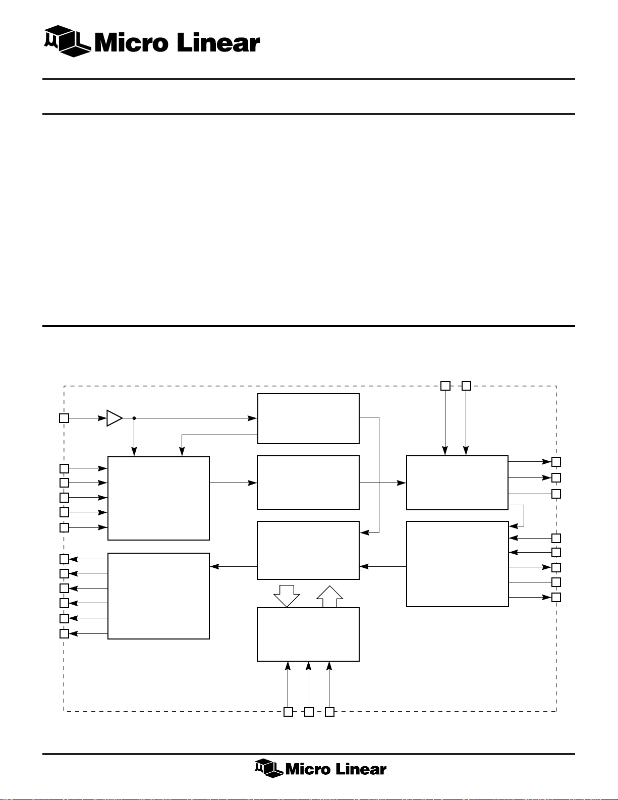
BLOCK DIAGRAM (PLCC Pin Configuration)
TXC
44
CLOCK SYTHESIZER
FEATURES
■ 5-bit (or symbol) parallel interface
■ Compliant to IEEE 802.3u 100BASE-TX standard
■ Compliant to ANSI X3T12 TP-PMD (FDDI) standard
■ Single-jack 10BASE-T/100BASE-TX solution when used
with external 10Mbps PHY
■ 125MHz receive clock recovery/generation
■ Baseline wander correction
■ Adaptive equalization and MLT-3 encoding/decoding
■ Supports full-duplex operation
*Some Packages Are End Of Life As Of August 1, 2000
41 40
10BTTXINP
10BTTXINN
TSM4
2
TSM3
3
TSM2
4
TSM1
5
TSM0
6
RXC
16
RSM4
8
RSM3
9
RSM2
11
RSM1
13
RSM0
15
SERIALIZER
DESERIALIZER
NRZ TO NRZI
AND
NRZI TO MLT-3
ENCODER
CLOCK AND DATA
RECOVERY
NRZI TO NRZ DECODER
CONTROL LOGIC
PWRDN
LPBK
SEL100/10
74225
100BASE-TX/10BASE-T
TWISTED PAIR DRIVER
EQUALIZER
BLW CORRECTION
MLT-3 DECODER
LOOPBACK MUX
TPOUTP
TPOUTN
CMREF
RGMSET
RTSET
TPINP
TPINN
SDO
34
33
31
38
37
39
30
24
1
ML6698
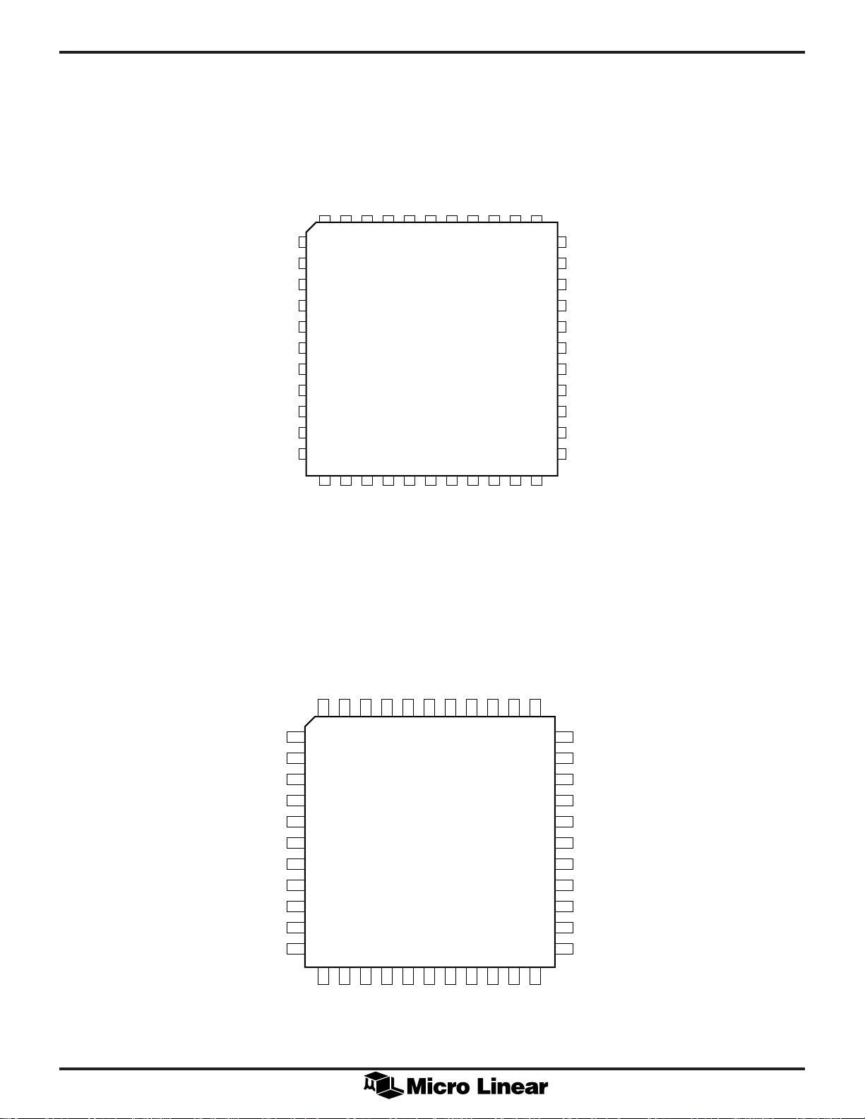
PIN CONFIGURATION
PWRDN
RSM4
RSM3
DGND1
RSM2
DVCC1
RSM1
DGND2
RSM0
RXC
DGND3
44-Pin PLCC (Q44)
TSM0
TSM1
TSM2
TSM3
65432
7
8
9
10
11
12
13
14
15
16
17
18 19 20 21 22
ML6698
TSM4
AGND1
TXC
AVCC1
LPBK
1442543264227412840
23 24
10BTTXINP
10BTTXINN
39
38
37
36
35
34
33
32
31
30
29
CMREF
TPINP
TPINN
AVCC2
AGND2
TPOUTP
TPOUTN
AGND3
RTSET
RGMSET
NC
PWRDN
RSM4
RSM3
DGND1
RSM2
DVCC1
RSM1
DGND2
RSM0
RXC
DGND3
DVCC2
DGND4B
DGND4A
44-Pin TQFP (H44-10)
TSM0
TSM1
TSM2
44 43 42 41 40
1
2
3
4
5
6
7
8
9
10
11
12 13 14 15 16
SDO
DVCC5
DGND5
DGND4C
ML6698
TSM3
TSM4
AGND1
TXC
39 381937203621352234
17 18
SEL100/10
AVCC1
NC
LPBK
NC
AVCC3
10BTTXINP
10BTTXINN
33
32
31
30
29
28
27
26
25
24
23
CMREF
TPINP
TPINN
AVCC2
AGND2
TPOUTP
TPOUTN
AGND3
RTSET
RGMSET
NC
NC
NC
AVCC3
SEL100/10
DVCC2
DGND4A
DGND4B
DGND4C
DVCC5
SDO
DGND5
2

ML6698
PIN DESCRIPTION
PIN NAME DESCRIPTION
1 (39) AGND1 Analog ground.
2-6 (40-44) TSM<4:0> Transmit data TTL inputs. TSM<4:0> inputs accept TX data symbols. Data
7 (1) PWRDN Device power down input. A low signal powers down all ciruits of the ML6698, and
8,9, (2, 3, RSM<4:0> Receive data TTL outputs. RSM<4:0> outputs may be sampled synchronously with
11,13, 5, 7, 9) RXC’s rising edge.
15
10 (4) DGND1 Digital ground.
12 (6) DVCC1 Digital +5V power supply.
14 (8) DGND2 Digital ground.
16 (10) RXC Recovered receive symbol clock TTL output. This 25MHz clock is phase-aligned
17 (11) DGND3 Digital ground.
18 (12) DVCC2 Digital +5V power supply.
19 (13) DGND4A Digital ground.
(Pin numbers for TQFP package in parentheses)
appearing at TSM<4:0> are clocked into the ML6698 on the rising edge of TXC.
dissipates less than 20mA.
with the internal 125MHz bit clock recovered from the signal received at TPINP/N
when data is present. Receive data at RSM<4:0> change on the falling edges and
should be sampled on the rising edges of this clock. RXC is phase aligned to TXC
when 100BASE-TX signal is not present at TPINP/N
20 (14) DGND4B Digital ground.
21 (15) DGND4C Digital ground.
22 (16) DVCC5 Digital +5V power supply.
23 (17) DGND5 Digital ground.
24 (18) SD0 Signal detect TTL output. A high output level indicates 100BASE-TX activity at
TPINP/N with an amplitude exceeding the preset threshold. The signal detect
function is always active independent of the configuration of the SEL100/10 pin.
25 (19) SEL100/10 Speed select TTL input. Driving this pin low disables 100BASE-TX transmit and
receive functions, and enables the 10BASE-T transmit path from 10BTTXINP/N to
TPOUTP/N. A high signal on SEL100/10 disables the 10BTTXINP/N inputs and enables
100BASE-TX operation.
28 (22) AVCC3 Analog positive power supply.
30 (24) RGMSET Equalizer bias resistor input. An external 9.53ký, 1% resistor connected between
RGMSET and AGND3 sets internal time constants controlling the receive equalizer
transfer function.
31 (25) RTSET Transmit level bias resistor input. An external 2.49ký, 1% resistor connected
between RTSET and AGND3 sets a precision constant bias current for the twisted
pair transmit level.
32 (26) AGND3 Analog ground.
33,34 (27,28) TPOUTN/P Transmit twisted pair outputs. This differential current output pair drives MLT-3
waveforms into the network coupling transformer in 100BASE-TX mode, and
10BASE-T or FLP waveforms in 10BASE-T mode.
35 (29) AGND2 Analog ground.
36 (30) AVCC2 Analog +5V power supply.
37,38 (31, 32) TPINN/P Receive twisted pair inputs. This differential input pair receives 100BASE-TX signals
from the network.
3

ML6698
PIN DESCRIPTION (Continued)
PIN NAME DESCRIPTION
39 (33) CMREF Receiver common-mode reference output. This pin provides a common-mode bias
point for the twisted-pair media line receiver. A typical value for CMREF is
(VCC–1.26)V.
40,41 (34,35) 10BTTXINN/P 10BASE-T transmit waveform inputs. The ML6698 presents a linear copy of the input
at 10BTTXINN/P to the TPOUTN/P outputs when the ML6698 functions in 10BASE-T
mode. Signals presented to these pins must be centered at VCC/2 with a single ended
amplitude of ± 0.25V.
42 (36) LPBK Loopback TTL input pin. Tying this pin to ground places the part in loopback mode;
data at RSM<4:0> are serialized, MLT-3 encoded, equalized then sent to the receive
PLL for clock recovery and sent to the RSM<4:0> outputs. Floating this pin or tying it
to VCC places the part in its normal mode of operation.
43 (37) AVCC1 Analog +5V power supply.
44 (38) TXC Transmit clock TTL input. This 25MHz clock is the frequency reference for the
internal transmit PLL clock multiplier. This pin should be driven by an external
25MHz clock at TTL or CMOS levels.
4
 Loading...