

Micro Linear Corporation ML6697CH, ML6697CQ Datasheet

July 1997
PRELIMINARY
ML6697
100BASE-TX Physical Layer with MII
GENERAL DESCRIPTION
The ML6697 implements the complete physical layer of
the Fast Ethernet 100BASE-TX standard. The ML6697
offers a single-chip per-port solution for MII-based
repeater applications. The ML6697 interfaces to the
controller through the Media Independent Interface (MII).
The ML6697 functionality includes 4B/5B encoding/
decoding, Stream Cipher scrambling/descrambling,
125MHz clock recovery/generation, receive adaptive
equalization, baseline wander correction, and MLT-3
transmitter.
BLOCK DIAGRAM (PLCC Package)
TXCLKIN
1
TXCLK
9
FEATURES
n Single-chip 100BASE-TX physical layer
n Compliant to IEEE 802.3u 100BASE-TX standard
n Supports MII-based repeater applications
n Compliant MII (Media Indendent Interface)
n 4B/5B encoder/decoder
n Stream Cipher scrambler/descrambler
n 125MHz clock recovery/generation
n Baseline wander correction
n Adaptive equalization and MLT-3 encoding/decoding
CLOCK SYNTHESIZER
TXD3
3
TXD2
4
TXD1
5
TXD0
6
TXEN
7
TXER
8
CRS
18
RXEN
19
RXCLK
17
RXD3
10
RXD2
12
RXD1
14
RXD0
16
RXDV
21
RXER
23
PCS TRANSMIT
STATE MACHINE
4B/5B ENCODER
SCRAMBLER
PCS RECEIVE
STATE MACHINE
5B/4B DECODER
DESCRAMBLER
NRZ TO NRZI ENCODER
SERIALIZER
MLT-3 ENCODER
CLOCK AND DATA
RECOVERY
NRZI TO NRZ DECODER
DESERIALIZER
MII MANAGEMENT REGISTERS
AND CONTROL LOGIC
MDIO
MDC
24
25
PHYAD1
PHYAD0
29
PHYAD233PHYAD4
30
31
PHYAD3
32
FLP/100BASE-TX
TWISTED PAIR DRIVER
EQUALIZER
BLW CORRECTION
MLT-3 DECODER
LOOPBACK MUX
TPOUTP
TPOUTN
RTSET
TPINP
TPINN
CMREF
RGMSET
LINK100
40
39
37
45
44
46
36
43
1
ML6697
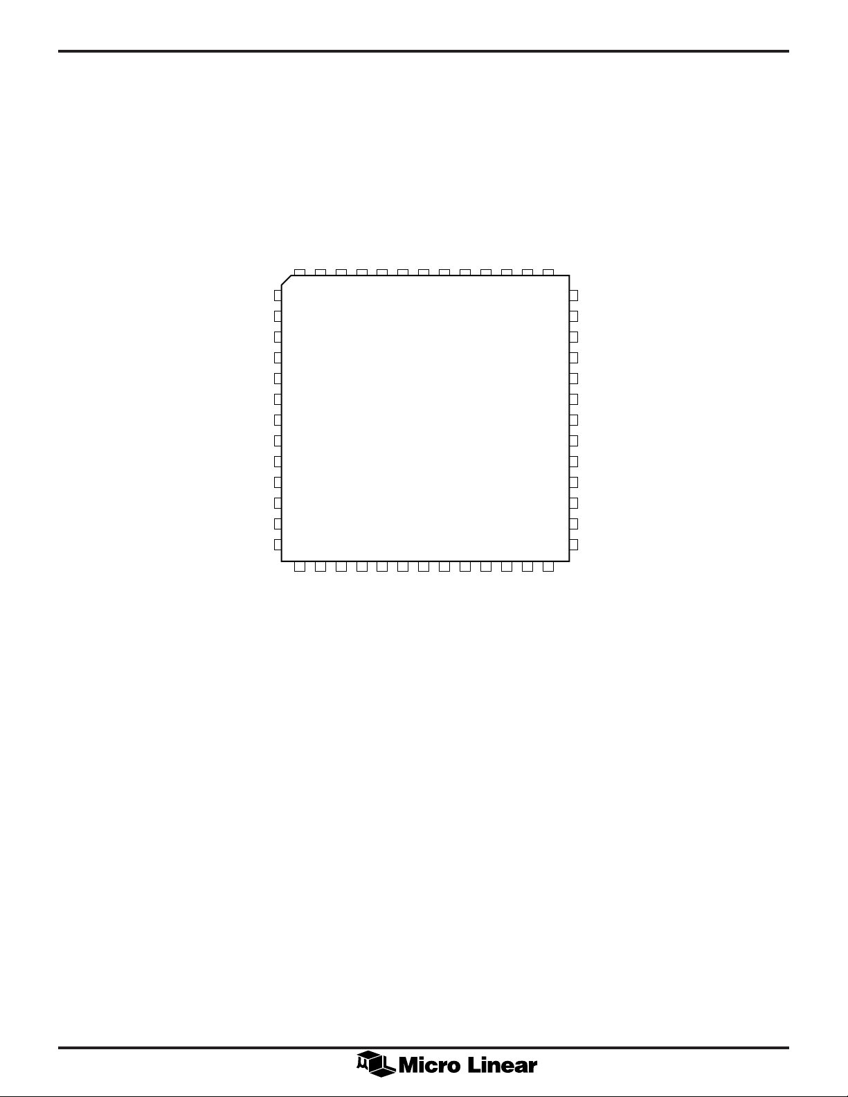
PIN CONFIGURATION
TXCLK
RXD3
DGND1
RXD2
DVCC1
RXD1
DGND2
RXD0
RXCLK
RXEN
DGND3
TXER
CRS
52-Pin PLCC (Q52)
TXEN
TXD0
TXD1
TXD2
76543
8
9
10
11
12
13
14
15
16
17
18
19
20
21 22 23 24 25
ML6697
TXD3
AGND1
TXCLKIN
AVCC1NCNCNCNC
21285229513050314932483347
26 27
NC
46
45
44
43
42
41
40
39
38
37
36
35
34
CMREF
TPINP
TPINN
LINK100
AVCC2
AGND2
TPOUTP
TPOUTN
AGND3
RTSET
RGMSET
AVCC3B
AVCC3A
RXDV
RXER
DVCC2
MDC
MDIO
DVCC5
DGND4
DGND5
PHYAD0
PHYAD1
PHYAD2
PHYAD3
PHYAD4
2
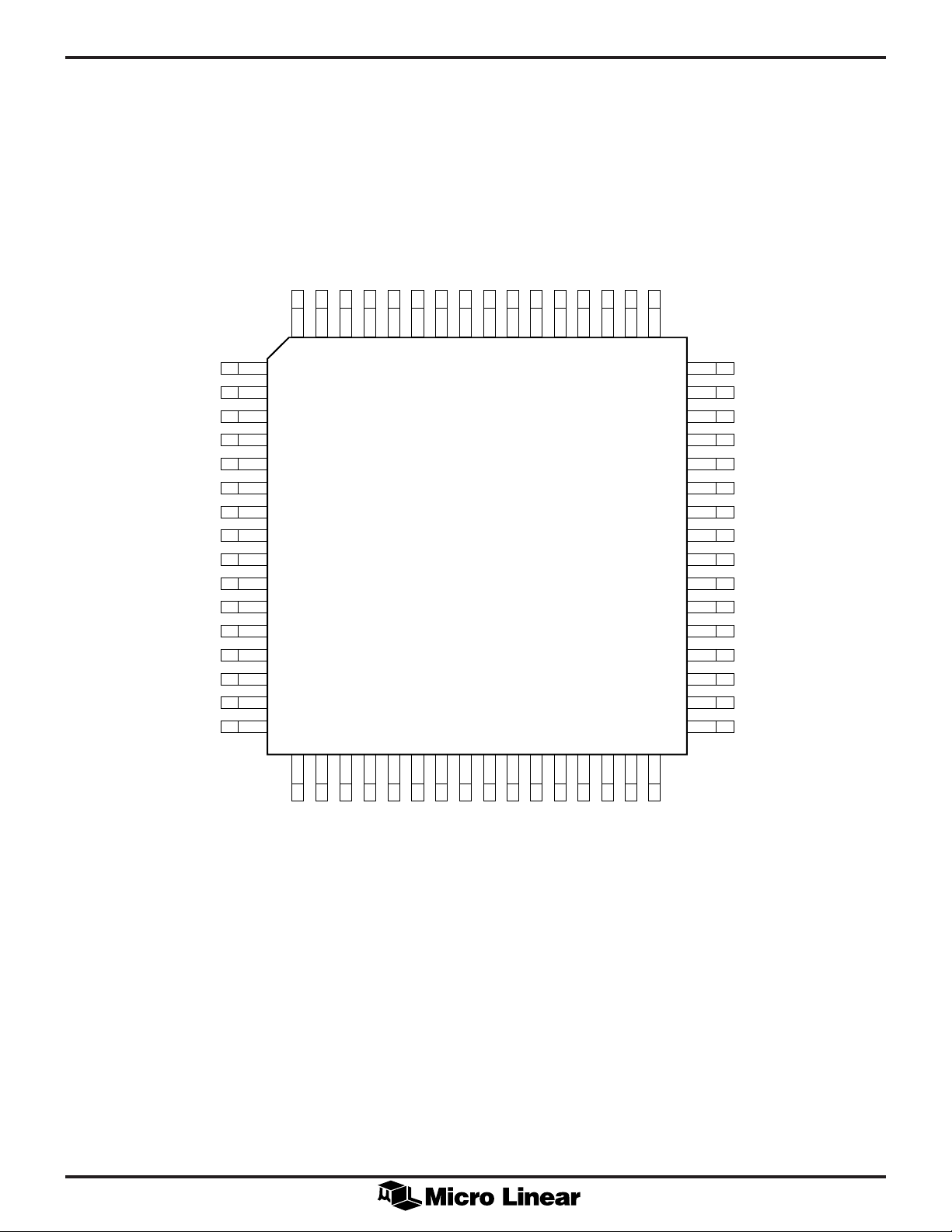
PIN CONFIGURATION (Continued)
TXER
TXEN
TXD0
64 63 62 61 60 59 58 57 56 55 54 53 52 51 50 49
TXCLK
RXD3
DGND1A
DGND1B
RXD2
DVCC1A
DVCC1B
RXD1
DGND2A
DGND2B
RXD0
RXCLK
CRS
RXEN
DGND3A
DGND3B
1
2
3
4
5
6
7
8
9
10
11
12
13
14
15
16
17 18 19 20 21 22 23 24 25 26 27 28 29 30 31 32
ML6697
64-Pin TQFP (H64-10)
TXD1
TXD2
TXD3
AGND1A
AGND1B
TXCLKIN
AVCC1NCNC
NC
NC
NC
NC
ML6697
48
47
46
45
44
43
42
41
40
39
38
37
36
35
34
33
NC
CMREF
TPINP
TPINN
LINK100
AVCC2
AGND2A
AGND2B
TPOUTP
TPOUTN
AGND3A
AGND3B
RTSET
RGMSET
AVCC3B
AVCC3A
RXDV
RXER
DVCC2
MDC
MDIO
DGND4B
DGND4A
DVCC5B
DVCC5A
DGND5B
DGND5A
PHYAD0
PHYAD1
PHYAD2
PHYAD3
PHYAD4
3

ML6697
PIN DESCRIPTION (Pin numbers for TQFP package in parentheses)
PIN NAME DESCRIPTION
1 (56) TXCLKIN Transmit clock TTL input. This 25MHz clock is the frequency reference for the
internal transmit PLL clock multiplier. This pin should be driven by an external
25MHz clock at TTL or CMOS levels.
2 (58, 57) AGND1 Analog ground.
3, 4 (59,60, TXD<3:0> Transmit data TTL inputs. TXD<3:0> inputs accept TX data from the MII. Data
5, 6 61,62) appearing at TXD<3:0> are clocked into the ML6697 on the rising edge of TXCLK.
7 (63) TXEN Transmit enable TTL input. Driving this input high indicates to the ML6697 that
transmit data are present at TXD<3:0>. TXEN edges should be synchronous with
TXCLK.
8 (64) TXER Transmit error TTL input. Driving this pin high with TXEN also high causes the part
to continuously transmit scrambled H symbols. When TXEN is low, TXER has no
effect.
9 (1) TXCLK Transmit clock TTL output. This 25MHz clock is phase-aligned with the internal
125MHz TX bit clock. Data appearing at TXD<3:0> are clocked into the ML6697 on
the rising edge of this clock.
10, 12, (2, 5, RXD<3:0> Receive data TTL outputs. RXD<3:0> outputs are valid on RXCLK’s rising edge.
14, 16 8, 11)
11 (3, 4) DGND1 Digital ground.
13 (6, 7) DVCC1 Digital +5V power supply.
15 (9, 10) DGND2 Digital ground.
17 (12) RXCLK Recovered receive clock TTL output. This 25MHz clock is phase-aligned with the
internal 125MHz bit clock recovered from the signal received at TPINP/N. Receive
data at RXD<3:0> changes on the falling edges and should be sampled on the rising
edges of this clock. RXCLK is phase aligned to TXCLKIN when the 100BASE-TX
signal is not present at TPINP/N.
18 (13) CRS Carrier Sense TTL output. CRS goes high in the presence of non-idle signals at TPINP/
N. CRS goes low when receive is idle.
19 (14) RXEN Receive enable TTL input. When this input is high, all the MII TTL outputs are
enabled. When this input is low, all the MII TTL outputs are in high impedance
mode. This input does not affect MDIO, TXCLK and CRS.
20 (15, 16) DGND3 Digital ground.
21 (17) RXDV Receive data valid TTL output. This output goes high when the ML6697 is receiving
a data packet. RXDV should be sampled synchronously with RXCLK’s rising edge.
22 (18) DVCC2 Digital +5V power supply.
23 (19) RXER Receive error TTL output. This output goes high to indicate error or invalid symbols
within a packet, or corrupted idle between packets. RXER should be sampled
synchronously with RXCLK’s rising edge.
24 (20) MDC MII Management Interface clock TTL input. A clock at this pin clocks serial data into
or out of the ML6697’s MII management registers through the MDIO pin. The
maximum clock frequency at MDC is 2.5MHz.
4

ML6697
PIN DESCRIPTION (Continued)
PIN NAME DESCRIPTION
25 (21) MDIO MII Management Interface data TTL input/output. Serial data are written to and read
from the ML6697’s management registers through this I/O pin. Input data is sampled
on the rising edge of MDC. Data output should be sampled synchronously with
MDC's rising edge.
26 (22, 23) DGND4 Digital ground.
27 (24, 25) DVCC5 Digital +5V power supply.
28 (26, 27) DGND5 Digital ground.
29 (28) PHYAD0 MII Serial Management Interface address bit 0.
30 (29) PHYAD1 MII Serial Management Interface address bit 1.
31 (30) PHYAD2 MII Serial Management Interface address bit 2.
32 (31) PHYAD3 MII Serial Management Interface address bit 3.
33 (32) PHYAD4 MII Serial Management Interface address bit 4.
34 (33) AVCC3A Analog +5V power supply.
35 (34) AVCC3B Analog +5V power supply.
36 (35) RGMSET Equalizer bias resistor input. An external 9.53kW, 1% resistor connected between
RGMSET and AGND3 sets internal time constants controlling the receive equalizer
transfer function.
37 (36) RTSET Transmit level bias resistor input. An external 2.49kW, 1% resistor connected between
RTSET and AGND3 sets a precision constant bias current for the twisted pair transmit
level.
38 (37, 38) AGND3 Analog ground.
39, 40 (39, 40) TPOUTN/P Transmit twisted pair outputs. This differential current output pair drives MLT-3
waveforms into the network coupling transformer.
41 (41, 42) AGND2 Analog ground.
42 (43) AVCC2 Analog +5V power supply.
43 (44) LINK100 100BASE-TX link activity open-drain output. LINK100 pulls low when there is
100BASE-TX activity at TPINP/N in 100BASE-TX or auto-negotiation modes. This
output is capable of driving an LED directly.
44, 45 (45, 46) TPINN/P Receive twisted pair inputs. This differential input pair receives 100BASE-TX signals
from the network.
46 (47) CMREF Receiver common-mode reference output. This pin provides a common-mode bias
point for the twisted-pair media line receiver, typically (VCC – 1.26)V.
52 (55) AVCC1 Analog +5V power supply.
5
 Loading...