

Micro Linear Corporation ML6696CH, ML6696CQ Datasheet
December 1998
ML6696*
100BASE-X Fiber Physical Layer
GENERAL DESCRIPTION
The ML6696 implements the complete physical layer of
the Fast Ethernet 100BASE-X standard for fiber media. The
device provides the MII (Media Independent Interface) for
interface to upper-layer silicon. The ML6696 integrates the
data quantizer and the LED driver, allowing the use of
low cost optical PMD components.
The ML6696 includes 4B/5B encoder/decoder, 125MHz
clock recovery/clock generation, LED driver, and a data
quantizer. The device also offers a power down mode
which results in total power consumption of less than 20mA.
The ML6696 is suitable for the current 100BASE-FX IEEE
803.2u standard defined using 1300nm optics, as well as
for the
proposed
100BASE-SX standard defined using lower
cost 820nm optics
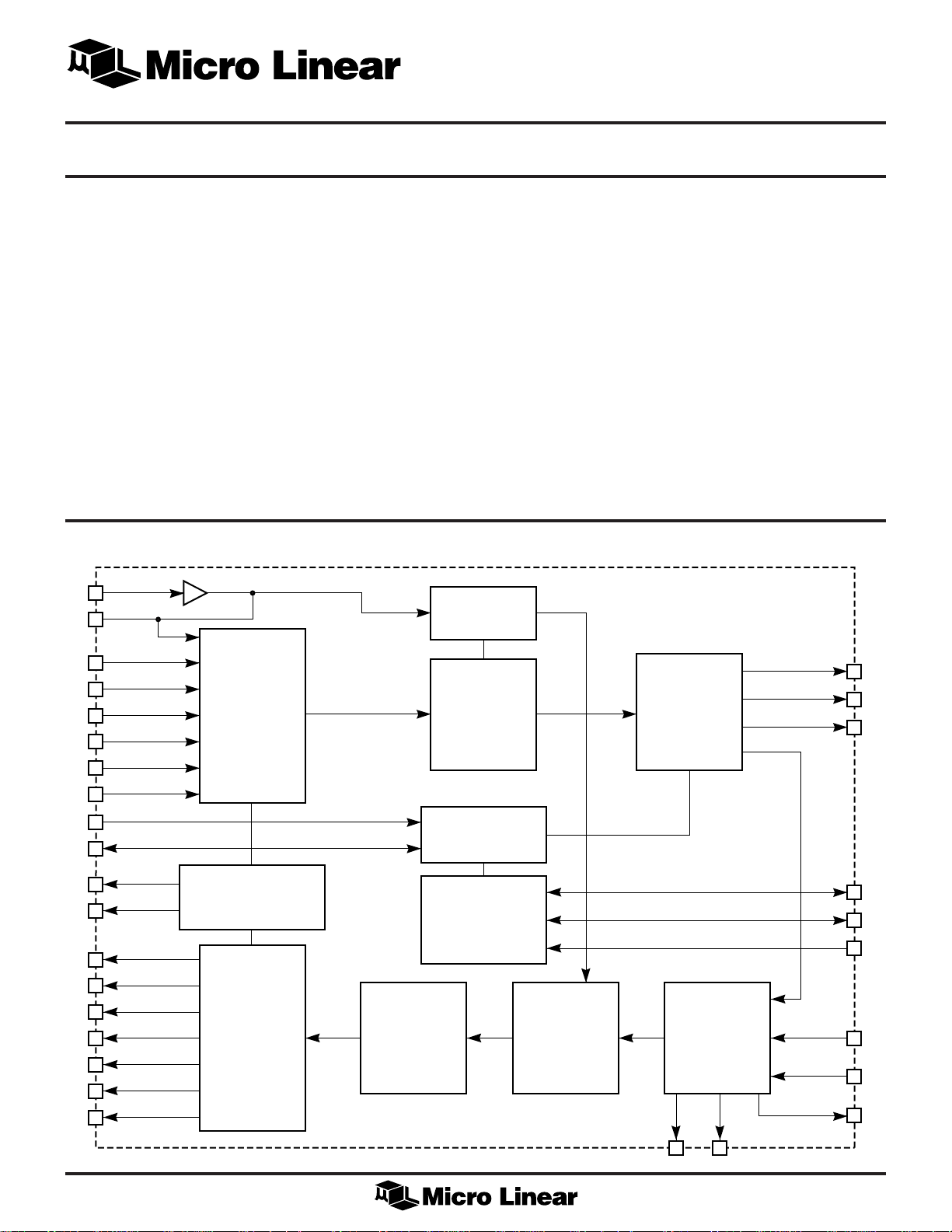
BLOCK DIAGRAM
CLKREF
TXCLK
TXER
TXEN
TXD3
TXD2
TXD1
TXD0
PCS
TRANSMIT
STATE
MACHINE
AND
4B/5B ENCODER
FEATURES
■ 100BASE-FX physical layer with MII
■ Optimal 100BASE-SX solution (draft standard)
■ Integrated data quantizer (post-amplifier)
■ Integrated LED driver
■ 125MHz clock generation and recovery
■ 4B/5B encoding/decoding
■ Power-down mode
* Some Packages Are Obsolete
CLOCK
SYNTHESIZER
SERIALIZER
NRZ TO NRZI
ENCODER
LED
DRIVER
IOUT
IOUT
RTSET
MDC
MDIO
COL
CRS
RXCLK
RXER
RXDV
RXD3
RXD2
RXD1
RXD0
CARRIER & COLLISION
LOGIC
PCS
RECEIVE
STATE
MACHINE
AND
4B/5B DECODER
DESERIALIZER
MII SERIAL
MANAGEMENT
INTERFACE
INITIALIZATION
INTERFACE
CLOCK & DATA
RECOVERY
NRZI TO NRZ
ENCODER
DATA QUANTIZER
(POST AMPLIFIER)
CAPDCCAPB
ECLK
EDIN
EDOUT
V
IN+
V
IN–
LINK100
1
ML6696
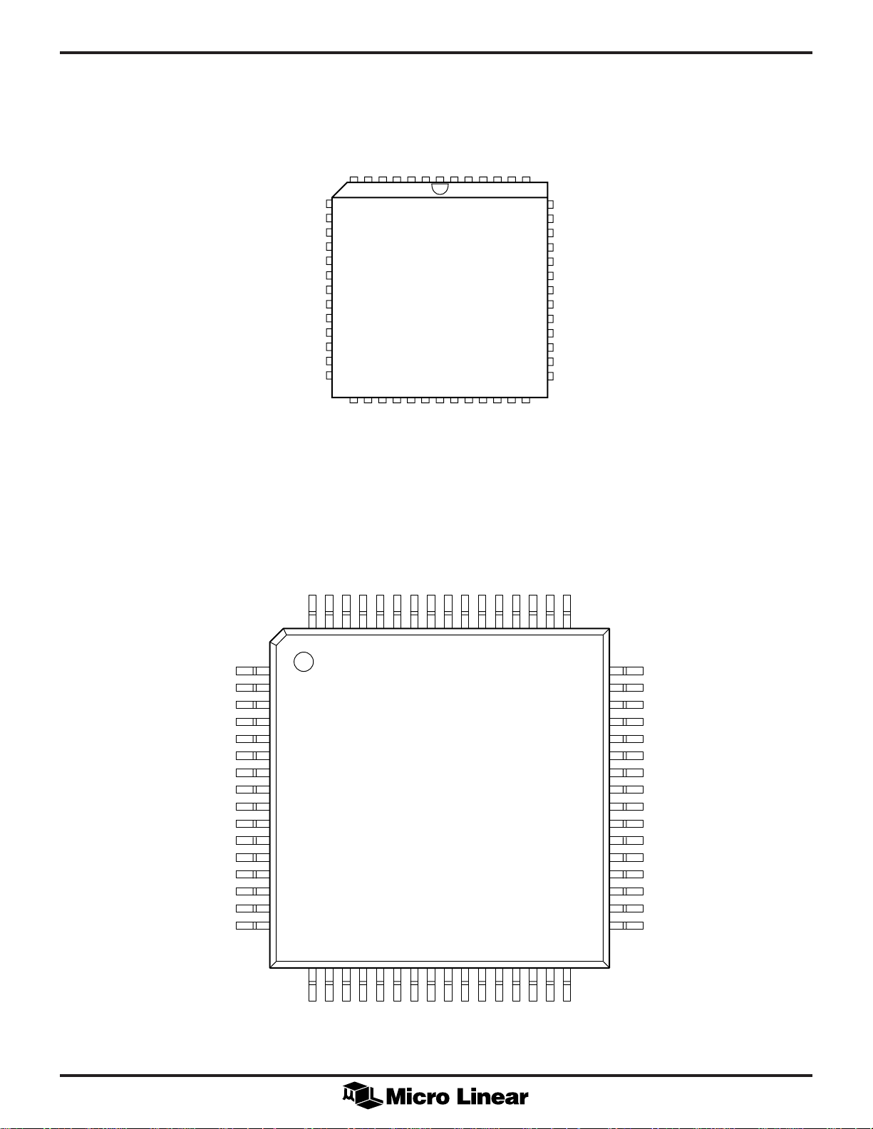
PIN CONFIGURATION
TXER
TXCLK
RXD3
DGND1
RXD2
DVCC1
RXD1
DGND2
RXD0
RXCLK
CRS
COL
DGND3
ML6696
52-Pin PLCC (Q52)
1
CC
EDIN
TXEN
TXD0
TXD1
TXD2
TXD3
AGND1
CLKREF
7654321525150494847
8
9
10
11
12
13
14
15
16
17
18
19
20
21 22 23 24 25 26 27 28 29 30 31 32 33
MDIO
DGND4
5
DV
2
RXDV
DV
CC
RXER
MDC
TOP VIEW
AV
CC
DGND5
NC
ECLK
NC
2
CC
EDOUT
AV
CAPB
CAPDC
AGND2
IOUT
46
45
IOUT
44
AGND3
43
RTSET
42
AVCC3A
41
AVCC3B
40
AVCC4A
39
AGND4A
38
LINK100
37
AVCC4B
36
AVCC4B
35
V
34
V
AGND4B
IN+
IN–
TXCLK
RXD3
DGND1
DGND1
DGND1
RXD2
DVCC1
RXD1
DGND2
DGND2
DGND2
RXD0
RXCLK
CRS
COL
DGND3
ML6696
64-Pin TQFP (H64-10)
1
TXER
TXEN
TXD0
TXD1
TXD2
TXD3
64 63 62 61 60 595857 56 55 54 535251 50 49
1
2
3
4
5
6
7
8
9
10
11
12
13
14
15
16
17 18
19 20 21 222324 25 26 27 282930 31 32
AGND1
CLKREF
AV
CC
EDIN
ECLK
EDOUT
AVCC2
AGND2
AGND2
AGND2
48
47
46
45
44
43
42
41
40
39
38
37
36
35
34
33
IOUT
IOUT
IOUT
IOUT
AGND3
AGND3
RTSET
AVCC3A
AVCC3B
AVCC4A
AGND4A
LINK100
AVCC4B
AVCC4B
V
IN+
V
IN–
RXDV
DGND3
2
CC
DV
RXER
MDC
MDIO
DGND4
5
CC
DV
DGND5
DGND5
NC
NC
CAPB
CAPDC
AGND4B
AGND4B
TOP VIEW
2

PIN DESCRIPTION (Pin Number in Parentheses is for PLCC Version)
ML6696
PIN NAME FUNCTION
1 (9) TXCLK Transmit clock TTL output. This
25MHz clock is phase-aligned
with the internal 125MHz TX bit
clock. Data appearing at
TXD<3:0> are clocked into the
ML6696 on the rising edge of this
clock.
2 (10) RXD3 Receive data TTL output. Output
is valid on RXCLK’s rising edge.
3, 4,
5, (11) DGND1 Digital ground
6 (12) RXD2 Receive data TTL output. Output
is valid on RXCLK’s rising edge.
7 (13) DVCC1 Digital positive power supply
8 (14) RXD1 Receive data TTL output. Output
is valid on RXCLK’s rising edge.
9, 10,
11 (15) DGND2 Digital ground
12 (16) RXD0 Receive data TTL output. Output
is valid on RXCLK’s rising edge.
13 (17) RXCLK Recovered receive clock TTL
output. This 25MHz clock is
phase-aligned with the internal
125MHz bit clock recovered from
the signal received at VIN+/-.
Receive data are clocked out at
RXD<3:0> on the falling edges of
this clock, and should be sampled
on rising edges. RXCLK is phasealigned to CLKREF in the absence
of a 100BASE-FX signal at V
14 (18) CRS Carrier Sense TTL output. CRS
goes high in the presence of nonidle signals at VIN+/-, or when the
ML6696 is transmitting. CRS goes
low when there is no transmit
activity and receive is idle. In
repeater or full-duplex mode, CRS
goes high in the presence of nonidle signals at V
15 (19) COL Collision Detected TTL output.
COL goes high upon detection of
a collision on the network, and
remains high as long as the
collision condition persists. COL is
low when the ML6696 operates in
full-duplex, repeater, or loopback
modes.
IN+/–
only.
IN+/–
PIN NAME FUNCTION
16, 17
(20) DGND3 Digital ground
18 (21) RXDV Receive data valid TTL output.
This output is high when the
ML6696 is receiving a data
packet. RXDV is valid on RXCLK’s
rising edge.
19 (22) DVCC2 Digital positive power supply
20 (23) RXER Receive error TTL output. This
output goes high to indicate error
or invalid symbols within a
packet, or corrupted idle between
packets. RXER is valid on RXCLK’s
rising edge.
21 (24) MDC MII Serial Management Interface
clock TTL input. A clock at this
pin clocks serial data into or out
of the ML6696’s MII management
registers through the MDIO pin.
The maximum clock frequency at
MDC is 2.5MHz.
22 (25) MDIO MII Serial Management Interface
data TTL input/output. Serial data
are written to and read from the
management registers through this
I/O pin. Input data is sampled on
the rising edge of MDC. Output
data is valid on MDC's rising edge
23 (26) DGND4 Digital ground
24 (27) DVCC5 Digital positive power supply
.
25, 26
(28) DGND5 Digital ground
27, 28
(29, 30) NC No connect
29 (31) CAPDC Data quantizer offset-correction
loop, offset-storage capacitor input
pin. The capacitor tied between
this pin and AVCC stores the
amplified data quantizer offset
voltage and also sets the dominant
pole in the offset-correction loop.
A 0.1µF surface mount is
recommended.
3

ML6696
PIN DESCRIPTION (Pin Number in Parentheses is for PLCC Version) (Continued)
PIN NAME FUNCTION
30 (32) CAPB Data quantizer input bias bypass
capacitor input. The capacitor tied
between this pin and AVCC filters
the quantizer’s internal input bias
reference. A 0.1µF surface-mount
capacitor is recommended.
31, 32
(33) AGND4B Analog ground
33 (34) V
34 (35) V
35, 36
(36, 37) AVCC4B Analog positive power supply
37 (38) LINK100 100BASE-FX link activity open-
38 (39) AGND4A Analog ground
39 (40) AVCC4A Analog positive power supply
40 (41) AVCC3B Analog positive power supply
41 (42) AVCC3A Analog positive power supply
42 (43) RTSET Transmit level bias resistor. For
43, 44
(44) AGND3 Analog ground
IN–
IN+
Receive quantizer negative input.
This input should be tied to
AVCCQ through an AC coupling
capacitor. (0.01µF recommended)
Receive quantizer positive input.
This input receives 100BASE-FX
signals from the network optical
receiver through an AC coupling
capacitor. (0.01µF recommended).
drain output. LINK100 pulls low
when there is 100BASE-FX activity
at VIN+/–. This output is capable
of sinking sufficient current to
directly drive a status LED in
series with a current limiting
resistor.
100BASE-FX, an external 2.32kW,
1% resistor connected between
RTSET and AGND3 sets a
precision constant bias current
that gives a nominal output "on"
current of 75mA at I
OUT
.
PIN NAME FUNCTION
47, 48
(46) IOUT Transmit LED output. This open-
collector current output drives
NRZI waveforms into a network
LED.
49, 50,
51 (47) AGND2 Analog ground
52 (48) AVCC2 Analog positive power supply
53 (49) EDOUT Initialization Interface data out
CMOS input. With EDIN low at
power up, EDOUT has no
function. With EDIN floating at
power up, EDOUT is the serial
data input for configuration data
from an EEPROM. With EDIN high
at power up, EDOUT is the input
for configuration data from an
external microcontroller. (Table 1)
54 (50) ECLK Initialization Interface clock
CMOS input/output. With EDIN
low at power up, ECLK is inactive.
With EDIN floating at power up,
ECLK is the ML6696’s clock
output for timing the configuration
data from an external EEPROM.
With EDIN high at power up,
ECLK is the clock input for timing
configuration data from an
external microcontroller. (Table 1)
55 (51) EDIN Initialization Interface mode
select and EEPROM interface data
in CMOS input/output. EDIN
selects one of three possible
interface modes at power up. See
the Initialization Interface section
for more information. (Table 1)
56 (52) AVCC1 Analog positive power supply
57 (1) CLKREF Transmit clock TTL input. This
25MHz clock is the frequency
reference for the internal TX PLL
clock synthesizer and logic. This
pin should be driven by an
external 25MHz clock at TTL
levels.
45, 46
(45) IOUT Transmit LED output. This pin
connects through an external 15W
resistor to AVCC when the part is
used to drive a network LED.
4
58 (2) AGND1 Analog ground
59 (3) TXD3 Transmit data TTL input. TXD<3:0>
inputs accept TX data symbols from
the MII. Data appearing at TXD<3:0>
are clocked into the ML6696 on the
rising edge of TXCLK.

PIN DESCRIPTION (Pin Number in Parentheses is for PLCC Version) (Continued)
ML6696
PIN NAME FUNCTION
60 (4) TXD2 Transmit data TTL input. TXD<3:0>
inputs accept TX data symbols
from the MII. Data appearing at
TXD<3:0> are clocked into the
ML6696 on the rising edge of
TXCLK.
61 (5) TXD1 Transmit data TTL input. TXD<3:0>
inputs accept TX data symbols
from the MII. Data appearing at
TXD<3:0> are clocked into the
ML6696 on the rising edge of
TXCLK.
62 (6) TXD0 Transmit data TTL input. TXD<3:0>
inputs accept TX data symbols
from the MII. Data appearing at
TXD<3:0> are clocked into the
ML6696 on the rising edge of
TXCLK.
PIN NAME FUNCTION
63 (7) TXEN Transmit enable TTL input. Driving
this input high indicates to the
ML6696 that transmit data are
present at TXD<3:0>. TXEN edges
should be synchronous with
TXCLK.
64 (8) TXER Transmit error TTL input. Driving
this pin high with TXEN also high
causes the part to continuously
transmit an H symbol (00100).
When TXEN is low, TXER has no
effect.
5
 Loading...