

Micro Linear Corporation ML6692CH, ML6692CQ Datasheet
April 1999
ML6692
100BASE-TX Physical Layer with MII
GENERAL DESCRIPTION
The ML6692 implements the complete physical layer of
the Fast Ethernet 100BASE-TX standard. The ML6692
interfaces to the controller through the standard-compliant
Media Independent Interface (MII). The ML6692
functionality includes auto-negotiation, 4B/5B encoding/
decoding, Stream Cipher scrambling/descrambling,
125MHz clock recovery/generation, receive adaptive
equalization, baseline wander correction, and MLT-3/
10BASE-T transmitter.
For applications requiring 100Mbps only, such as
repeaters, the ML6692 offers a single-chip per-port
solution. For 10/100 dual speed adapters or switchers,
10BASE-T functionality may be attained using Micro
Linear’s ML2653, or by using an Ethernet controller that
contains an integrated 10BASE-T PHY.
FEATURES
■ Single-chip 100BASE-TX physical layer
■ Compliant to IEEE 802.3u 100BASE-TX standard
■ Supports adapter, repeater and switch applications
■ Single-jack 10BASE-T/100BASE-TX solution when used
with external 10Mbps PHY
■ Compliant MII (Media Independant Interface)
■ Auto-negotiation capability
■ 4B/5B encoder/decoder
■ Stream Cipher scrambler/descrambler
■ 125MHz clock recovery/generation
■ Baseline wander correction
■ Adaptive equalization and MLT-3 encoding/decoding
■ Supports full-duplex operation
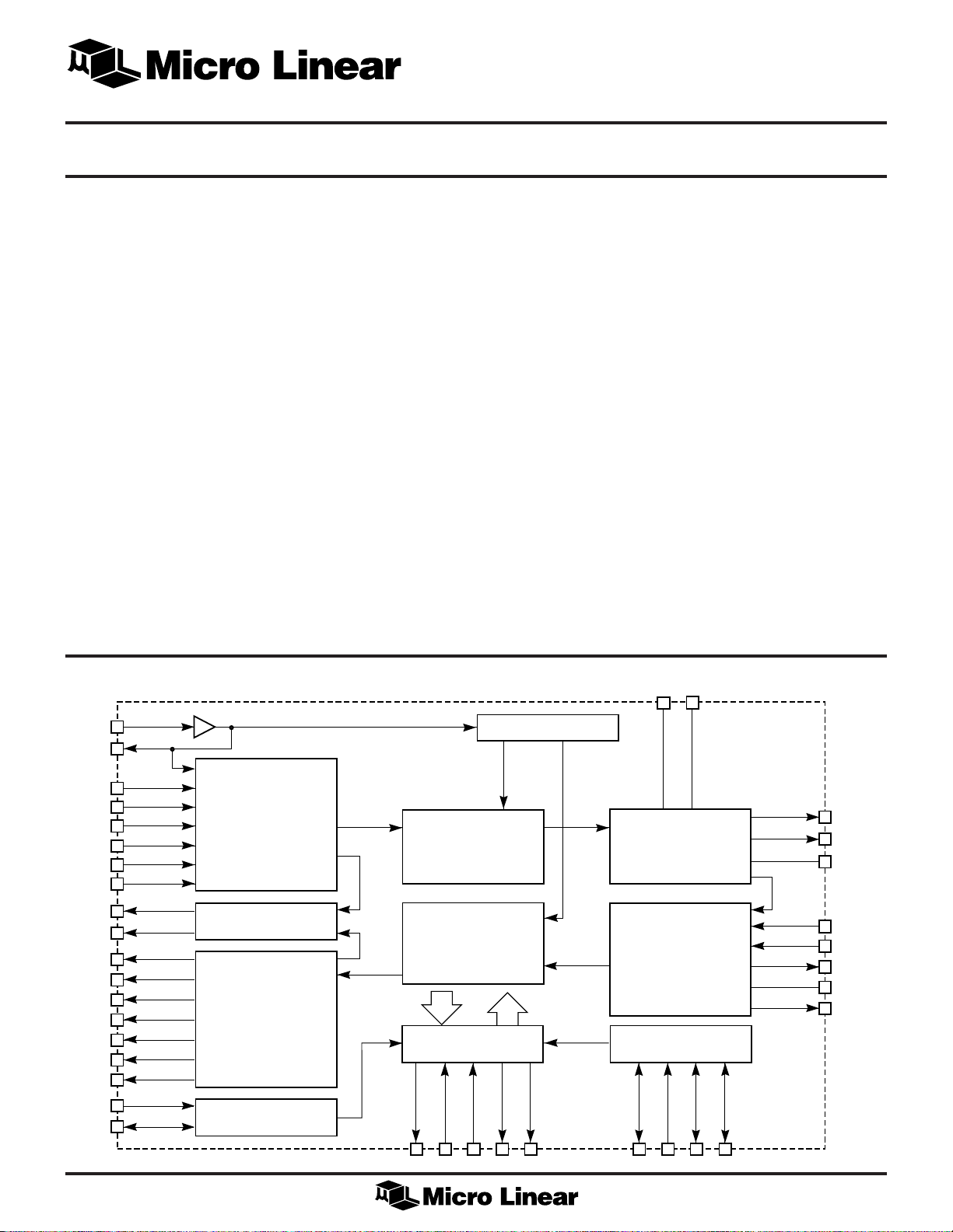
BLOCK DIAGRAM (PLCC Package)
TXCLKIN
1
TXCLK
9
TXD3
3
TXD2
4
TXD1
5
TXD0
6
TXEN
7
TXER
8
CRS
18
COL
19
RXCLK
17
RXD3
10
RXD2
12
RXD1
14
RXD0
16
RXDV
21
RXER
23
MDC
24
MDIO
25
PCS TRANSMIT
STATE MACHINE
4B/5B ENCODER
SCRAMBLER
CARRIER AND
COLLISION LOGIC
PCS RECEIVE
STATE MACHINE
5B/4B DECODER
DESCRAMBLER
MII MANAGEMENT
REGISTERS
CLOCK SYNTHESIZER
NRZ TO NRZI ENCODER
SERIALIZER
MLT-3 ENCODER
CLOCK AND DATA
RECOVERY
NRZI TO NRZ DECODER
DESERIALIZER
AUTO-NEGOTIATION
AND CONTROL LOGIC
T4EN
T4FAIL
29 30
10BTLNKEN
10BTRCV
50 51
DUPLEX
47
48
49
10BTTXINP
10BTTXINN
FLP/100BASE-TX/10BASE-T
TWISTED PAIR DRIVER
EQUALIZER
BLW CORRECTION
MLT-3 DECODER
LOOPBACK MUX
INITIALIZATION
REGISTER
EDIN
31
SEL10HD
32
33
SEL10FD
/ECLK
35
TPOUTN
LINK100
SEL100T4
/EDOUT
TPOUTP
RTSET
TPINP
TPINN
CMREF
RGMSET
40
39
37
45
44
46
36
43
1

ML6692
PIN CONFIGURATION
TXER
TXCLK
RXD3
DGND1
RXD2
DVCC1
RXD1
DGND2
RXD0
RXCLK
CRS
COL
DGND3
ML6692
52-Pin PLCC (Q52)
TXEN
TXD0
TXD1
TXD2
TXD3
AGND1
TXCLKIN
AVCC1
10BTLNKEN
10BTRCV
7654321525150494847
8
9
10
11
12
13
14
15
16
17
18
19
20
21 22 23 24 25 26 27 28 29 30 31 32 33
RXER
RXDV
DVCC2
MDC
MDIO
DGND4
TOP VIEW
DVCC5
T4EN
DGND5
T4FAIL
10BTTXINP
10BTTXINN
DUPLEX
46
45
44
43
42
41
40
39
38
37
36
35
34
EDIN
SEL10HD
SEL 10FD/ECLK
CMREF
TPINP
TPINN
LINK100
AVCC2
AGND2
TPOUTP
TPOUTN
AGND3
RTSET
RGMSET
SEL100T4/EDOUT
AVCC3
2
PIN CONFIGURATION
ML6692
64-Pin TQFP (H64-10)
TXER
TXEN
TXD0
TXD1
TXD2
TXD3
AGND1A
AGND1B
TXCLKIN
AVCC1
10BTLNKEN
10TRCVNC10BTTXINP
64 63 62 61 60 595857 56 55 54 535251 50 49
10TTXINN
ML6692
NC
TXCLK
RXD3
DGND1A
DGND1B
RXD2
DVCC1A
DVCC1B
RXD1
DGND2A
DGND2B
RXD0
RXCLK
CRS
COL
DGND3A
DGND3B
1
2
3
4
5
6
7
8
9
10
11
12
13
14
15
16
17 18
19 20 21 222324 25 26 27 282930 31 32
RXER
RXDV
DVCC2
MDC
MDIO
DGND4B
DGND4A
DVCC5B
DVCC5A
DGND5B
DGND5A
T4EN
EDIN
T4FAIL
TOP VIEW
48
47
46
45
44
43
42
41
40
39
38
37
36
35
34
33
SEL10HD
SEL10FD/ECLK
DUPLEX
CMREF
TPINP
TPINN
LINK100
AVCC2
AGND2A
AGND2B
TPOUTP
TPOUTN
AGND3A
AGND3B
RTSET
RGMSET
SEL100T4/EDOUT
AVCC3
3

ML6692
PIN DESCRIPTION (Pin Numbers for TQFP package in parentheses)
PIN NAME FUNCTION
1 (56) TXCLKIN Transmit clock TTL input. This 25MHz clock is the frequency reference for the internal
transmit PLL clock multiplier. This pin should be driven by an external 25MHz clock at
TTL or CMOS levels.
2 (57, 58) AGND1 Analog ground.
3, 4, 5, 6, TXD<3:0> Transmit data TTL inputs. TXD<3:0> inputs accept TX data from the MII. Data
(59, 60, 61, 62) appearing at TXD<3:0> are clocked into the ML6692 on the rising edge of TXCLK.
7 (63) TXEN Transmit enable TTL input. Driving this input high indicates to the ML6692 that transmit
data are present at TXD<3:0>. TXEN edges should be synchronous with TXCLK.
8 (64) TXER Transmit error TTL input. Driving this pin high with TXEN also high causes the part to
continuously transmit scrambled H symbols. When TXEN is low, TXER has no effect.
9 (1) TXCLK Transmit clock TTL output. This 25MHz clock is phase-aligned with the internal 125MHz
TX bit clock. Data appearing at TXD<3:0> are clocked into the ML6692 on the rising
edge of this clock.
10, 12, 14, 16 RXD<3:0> Receive data TTL outputs. RXD<3:0> outputs are valid on RXCLK’s rising edge.
(2, 5, 8, 11)
11 (3, 4) DGND1 Digital ground.
13 (6, 7) DVCC1 Digital +5V power supply.
15 (9, 10) DGND2 Digital ground.
17 (12) RXCLK Recovered receive clock TTL output. This 25MHz clock is phase-aligned with the
internal 125MHz bit clock recovered from the signal received at TPINP/N. Receive data
at RXD<3:0> changes on the falling edges and should be sampled on the rising edges of
this clock. RXCLK is phase aligned to TXCLKIN when the 100BASE-TX signal is not
present at TPINP/N.
18 (13) CRS Carrier Sense TTL output. For 100Mbps operation in standard mode, CRS goes high in the
presennon-idle signals at TPINP/N, or when the ML6692 is transmitting. CRS goes low when
there is no transmit activity and receive is idle. For 100 Mbps operation in repeater mode
or half duplex mode, CRS goes high in the presence of non-idle signals at TPINP/N only.
19 (14) COL Collision Detected TTL output. For 100 Mbps operation COL goes high upon detection of
a collision on the network, and remains high as long as the collision condition persists.
COL is low when the ML6692 operates in either full duplex, or loopback modes.
20 (15, 16) DGND3 Digital ground.
21 (17) RXDV Receive data valid TTL output. This output goes high when the ML6692 is receiving a
data packet. RXDV should be sampled synchronously with RXCLK’s rising edge.
22 (18) DVCC2 Digital +5V power supply.
23 (19) RXER Receive error TTL output. This output goes high to indicate error or invalid symbols
within a packet, or corrupted idle between packets. RXER should be sampled
synchronously with RXCLK’s rising edge.
24 (20) MDC MII Management Interface clock TTL input. A clock at this pin clocks serial data into or
out of the ML6692’s MII management registers through the MDIO pin. The maximum clock
frequency at MDC is 2.5MHz.
4

ML6692
PIN DESCRIPTION (Continued)
PIN NAME FUNCTION
25 (21) MDIO MII Management Interface data TTL input/output. Serial data are written to and read
from the ML6692’s management registers through this I/O pin. Input data is sampled on the
rising edge of MDC. Data output should be sampled synchronously with MDC's rising
edge.
26 (22, 23) DGND4 Digital ground.
27 (24, 25) DVCC5 Digital +5V power supply.
28 (26, 27) DGND5 Digital ground.
29 (28) T4EN 100BASE-T4 enable TTL output. This output goes low if the auto-negotiation function
chooses 100BASE-T4 as the highest common denominator technology. This output is high
on power-up, during auto-negotiation, when the ML6692 enables any other protocol, or
when 100BASE-T4 technology is not supported. If auto-negotiation is disabled, T4EN is
always low.
30 (29) T4FAIL 100BASE-T4 link fail TTL input. When driven high, it indicates a good, 100BASE-T4 link.
When the auto-negotiation function chooses 100BASE-T4 as the highest common
denominator technology, and indicates it by driving T4EN low, T4FAIL should go high
within 750-1000ms; otherwise auto-negotiation is restarted. Driving this pin low after autonegotiation is completed, also restarts it. In the parallel detection function, driving this pin
high indicates that the 100BASE-T4 link is ready. If auto-negotiation is disabled and
management register bit 0.13 is set to 1 (100Mb/s data rate selected), driving T4FAIL
high indicates a valid 100BASE-T4 link and disables the ML6692’s 100BASE-TX analog
functions. If bit 13 of the MII Control register is set to 0, T4FAIL has no effect.
31 (30) EDIN Initialization interface mode select and EEPROM interface mode data-in CMOS
input/output. EDIN selects one of three possible interface modes at power up. See table
on page 14 for more detail
32 (31) SEL10HD Initialization Interface 10BASE-T half duplex CMOS input. When EDIN is high or
floating, this pin has no effect. When EDIN is low, this pin sets the value of bit 11 of the
MII Status register (10Mb/s half duplex), and the default value of bit 5 of the MII
Advertisment register (10BASE-T half duplex capability).
33 (32) SEL10FD/ Initialization Interface 10BASE-T full duplex CMOS input/clock CMOS input/output. ECLK
ECLK When EDIN is low, this pin sets the value of bit 12 of the MII Status register (10Mb/s full
duplex), and the default value of bit 6 of the MII Advertisement register (10BASE-T full
duplex capability). When EDIN is left floating, this pin provides the output clock to read
initialization data from an external EEPROM. When EDIN is high, this pin is the input
clock to load data from an external microcontroller.
34 (33) AVCC3 Analog +5V power supply.
35 (34) SEL100T4/ Initialization Interface 100BASE-T4 CMOS input and EEPROM or microcontroller
EDOUT data-out CMOS input. When EDIN is low, this pin sets the value of bit 15 of the MII
Status register (100BASE-T4), and the default value of bit 9 of the MII Advertisement
register (100BASE-T4 capability). When EDIN is floating, this pin is the initialization
data input from an external EEPROM. When EDIN is high, this pin is the initialization
data input from a microcontroller.
36 (35) RGMSET Equalizer bias resistor input. An external 9.53ký, 1% resistor connected between
RGMSET and AGND3 sets internal time constants controlling the receive equalizer
transfer function.
5

ML6692
PIN DESCRIPTION (Continued)
37 (36) RTSET Transmit level bias resistor input. An external 2.49kW, 1% resistor connected between
RTSET and AGND3 sets a precision constant bias current for the twisted pair transmit
level.
38 (37, 38) AGND3 Analog ground.
39, 40 (39, 40) TPOUTN/P Transmit twisted pair outputs. This differential current output pair drives FLP waveforms
and MLT-3 waveforms into the network coupling transformer in 100BASE-TX mode, or
10BASE-T waveforms in 10BASE-T mode.
41 (41, 42) AGND2 Analog ground.
42 (43) AVCC2 Analog +5V power supply.
43 (44) LINK100 100BASE-TX link activity open-drain output. LINK100 pulls low when there is 100BASE-
TX activity at TPINP/N in 100BASE-TX or auto-negotiation modes. This output is capable
of driving an LED directly.
44, 45 (45, 46) TPINN/P Receive twisted pair inputs. This differential input pair receives 100BASE-TX, FLP, or
10BASE-T signals from the network.
46 (47) CMREF Receiver common-mode reference output. This pin provides a common-mode bias point
for the twisted-pair media line receiver, typically (VCC – 1.26)V.
47 (48) DUPLEX Full duplex enabled TTL output. This output is high during the auto-negotiation process,
it’s low when auto-negotiation is reset (power-up, reset bit, restart auto-negotiation bit,
power down bit, or link loss) and follows the duplex status otherwise. It drives the
ML2653’s FD input, and prevents the ML2653 from attempting to transmit during autonegotiation. For 10BASE-T transceivers without pin-selectable MAU loopback disable,
DUPLEX can be used to disable the 10BASE-T transceiver’s receive and collision outputs
to the controller during auto-negotiation.
48, 49 (50, 51) 10BTTXINN/P 10BASE-T transmit waveform inputs. The ML6692 presents a linear copy of the input at
10BTTXINP/N to the TPOUTP/N outputs when the ML6692 functions in 10BASE-T mode.
Signals presented to these pins must be centered at VCC/2 and have a single ended
amplitude of ±0.25V.
50 (53) 10BTRCV 10BASE-T receive activity TTL input. The external 10BASE-T transceiver drives this pin
high to indicate 10BASE-T packet reception from the network.
51 (54) 10BTLNKEN 10BASE-T link control TTL output. This output is low if the ML6692 is in 10BASE-T mode,
or if the auto-negotiation function indicates to the 10BASE-T PMA to scan for carrier. This
output is high if the 10BASE-T PMA should be disabled.
52 (55) AVCC1 Analog +5V power supply.
6

ABSOLUTE MAXIMUM RATINGS
ML6692
Absolute maximum ratings are those values beyond which
the device could be permanently damaged. Absolute
maximum ratings are stress ratings only and functional
device operation is not implied.
Lead Temperature (Soldering, 10 sec) .....................260°C
Thermal Resistance (qJA)
PLCC ............................................................... 40°C/W
TQFP ............................................................... 52°C/W
VCC Supply Voltage Range .................. GND –0.3V to 6V
Input Voltage Range
OPERATING CONDITIONS
Digital Inputs ...................... GND – 0.3V to VCC +0.3V
TPINP, TPINN, 10BTTXNP, 10BTTXINN, .......................
........................................... GND –0.3V to VCC +0.3V
Output Current
TPOUTP, TPOUTN .............................................. 60mA
All other outputs ................................................. 10mA
Junction Temperature .............................................. 150°C
Storage Temperature .............................–65°C to +150°C
VCC Supply Voltage............................................ 5V ±5%
All VCC supply pins must be within 0.1V of each other.
All GND pins must be within 0.1V of each other.
TA , Ambient temperature.............................. 0ºC to 70°C
RGMSET .................................................... 9.53kW ± 1%
RTSET ........................................................ 2.49kW ± 1%
Receive transformer insertion loss ...................... <–0.5dB
DC ELECTRICAL CHARACTERISTICS
Over full range of operating conditions unless otherwise specified (Note 1).
SYMBOL PARAMETER CONDITIONS MIN TYP MAX UNITS
RECEIVER
V
ICM
TPINP/N Input Common-Mode VCC – 1.26 V
Voltage (CMREF)
V
R
IDR
I
ICM
I
RGM
I
LED OUTPUT (LINK100)
I
OLS
I
OHS
TRANSMITTER
I
TD100
I
TD10
I
TOFF
I
TXI
TPINP-TPINN Differential Input –3.0 3.0 V
ID
Voltage Range
TPINP-TPINN Differential 10.0k W
Input Resistance
TPINP/N Common-Mode Input Current +10 µA
RGMSET Input Current RGMSET = 9.53kW 130 µA
RTSET Input Current RTSET = 2.49kW 500 µA
RT
Output Low Current 5mA
Output Off Current 10 µA
TPOUTP/N 100BASE-TX Mode Note 2, 3 ±19 ±21 mA
Differential Output Current
TPOUTP/N 10BASE-T ±55 ±60 ±65 mA
Mode Differential Output Current
TPOUTP/N Off-State Output RL = 200, 1% 0 1.5 mA
TPOUTP/N Differential Output
Current Imbalance RL = 200, 1% 500 µA
7
 Loading...