

Micro Linear Corporation ML6691CQ Datasheet
March 1997
ML6691*
100BASE-T MII-to-PMD Transceiver
GENERAL DESCRIPTION
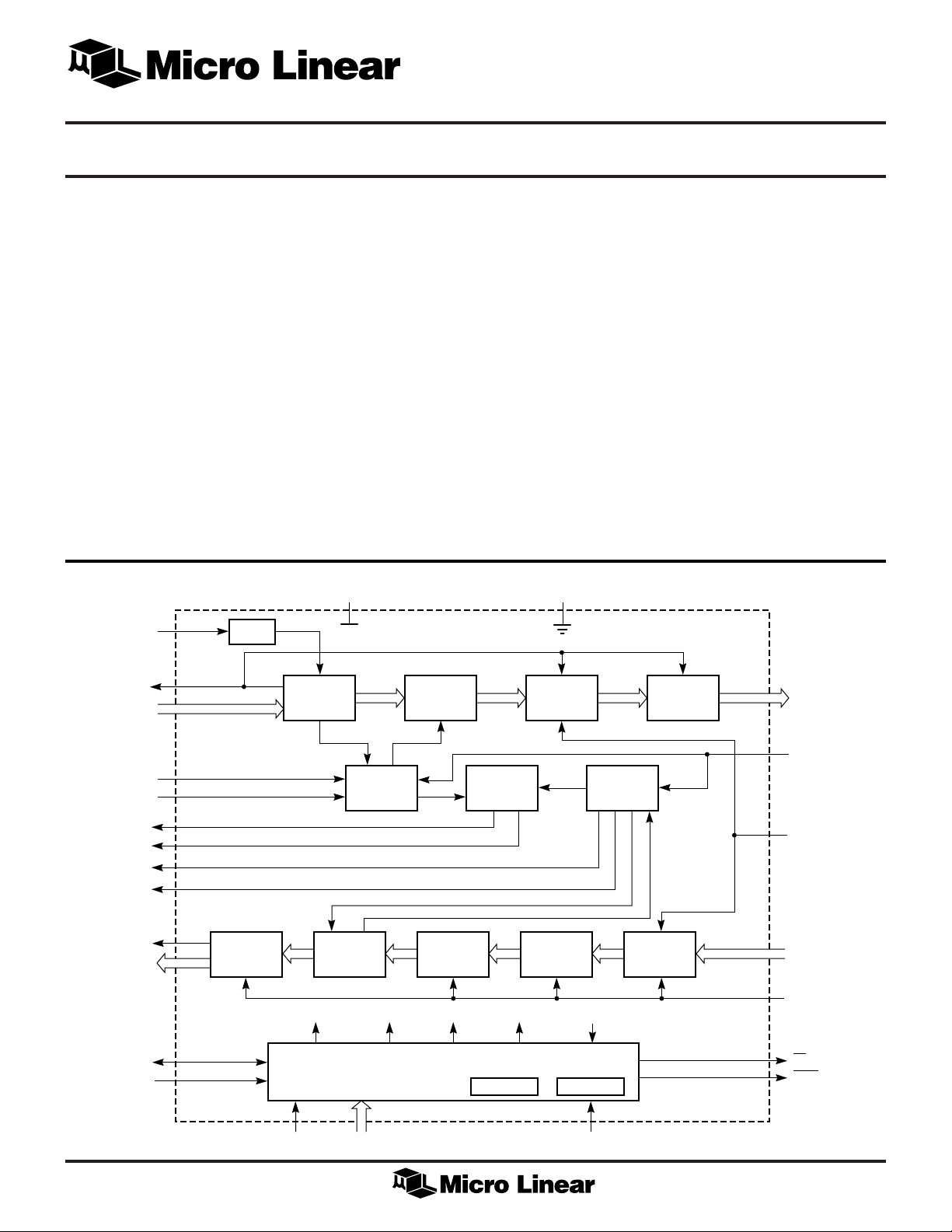
The ML6691 implements the upper portion of the physical
layer for the Fast Ethernet 100BASE-T standard. Functions
contained in the ML6691 include a 4B/5B encoder/
decoder, a Stream Cipher scrambler/descrambler, and
collision detect. Additional functions of the ML6691 —
accessible through the two-wire MII management
interface — include full duplex operation, loopback,
power down mode, and MII isolation.
The ML6691 is designed to interface to a 100BASE-T
Ethernet Media Access Controller (MAC) via the MII
(Media Independent Interface) on one side, and a
100BASE-X PMD transceiver on the other side. A
complete 100BASE-TX physical layer (PHY) solution is
realized using the ML6691, the ML6673, and one of the
available clock recovery/generation devices. A 100BASE-
FEATURES
■ Conforms to the Fast Ethernet 100BASE-T
IEEE 802.3µ standard
■ Integrated 4B/5B encoder/decoder
■ Integrated Stream Cipher scrambler/descrambler
■ Compliant MII interface
■ Two-wire serial interface management port for
configuration and control
■ On-chip 25 MHz crystal oscillator
■ Interfaces to either AMD’s PDT/PDR (AM79865/79866)
or Motorola’s FCG (MC68836)
■ Used with ML6673 for 100BASE-TX solutions
■ 44-pin PLCC package
FX physical layer solution is implemented by disabling the
scrambler function of the ML6691 and using an external * This Part Is End Of Life As Of August 1, 2000
optical PMD.
BLOCK DIAGRAM
TXC
OSC
V
CC
GND
TXCLK
TXD3
TXD0
TXEN
TXER
COL
CRS
RXDV
RXER
RXCLK
RXD3
RXD0
MDIO
MDC
NIBBLE
INPUT
...
NIBBLE
...
OUTPUT
REGISTER
REGISTER
TRANSMIT
STATE
MACHINE
5B/4B
DECODER
ISOLATE FULLDUP COLTST LPBK LINK FAILED
4B/5B
ENCODER
COLLISION
DETECTION
SYMBOL
ALIGNER
MANAGEMENT SECTION
CONTROL STATUS
STREAM
CIPHER
SCRAMBLER
STREAM
CIPHER
DESCRAMBLER
RECEIVE
STATE
MACHINE
SYMBOL
OUTPUT
REGISTER
SYMBOL
INPUT
REGISTER
TSM4
...
TSM0
SD
DCFR
RSM4
...
RSM0
RXC
CS
LPBK
LOCAL AD4...AD0 RST
1
ML6691
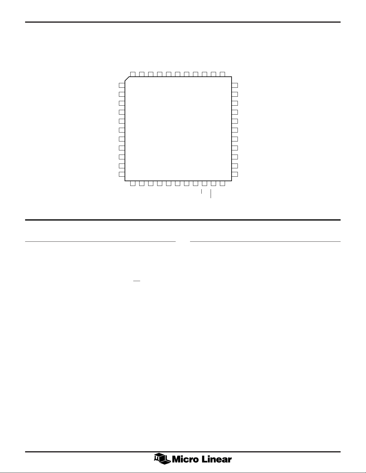
PIN CONFIGURATION
TXD3
TXD2
TXD1
TXD0
RXD3
RXD2
RXD1
RXD0
TXER
CRS
COL
TXEN
TXCLK
65432
7
8
9
10
11
12
13
14
15
16
17
18 19 20 21 22
RXER
RXDV
ML6691
44-PIN PLCC (Q44)
AD4
AD3
AD2
VCCAD1
1442543264227412840
23 24
CC
V
GND
DCFR
RXCLK
LOCAL
AD0
RST
MDC
CS
MDIO
LPBK
TXC
RXC
39
TSM4
38
TSM3
37
TSM2
36
TSM1
35
TSM0
34
SD
33
RSM4
32
RSM3
31
RSM2
30
RSM1
29
RSM0
PIN DESCRIPTION
PIN# NAME FUNCTION
1,21 V
CC
2,3,4, AD[4:0] Local PHY address. These 5 inputs set
43,44 the address to which the local physical
5 TXCLK Transmit clock output. Continuous
6 TXEN Transmit enable input. A logic high
7 TXER Transmit error input. When TXER is
8-11 TXD[3:0] Transmit nibble data inputs. Nibble-
Positive 5 volt supply.
layer responds. When an address
match is detected, the CS output is
asserted.
25MHz clock provides the timing
reference for the transfer of TXEN,
TXER, and TXD[3:0] from the MAC.
TXCLK is generated from the TXC
input.
enables the transmit section of the
ML6691. This signal indicates the
MAC is transmitting nibble-wide data.
TXEN is synchronous to TXCLK.
high , while TXEN is asserted, the
ML6691 will insert an “H” symbol in
the data stream. TXER is synchronous
to TXCLK.
wide data from the MAC. For data
transmission TXEN must be asserted.
TXD[0] is the least significant bit.
TXD[3:0] is synchronous to TXCLK.
PIN# NAME FUNCTION
12 CRS Carrier sense output. A logic high
indicates that either the transmit or
receive medium is non-idle. CRS is
deasserted when both transmit and
receive are idle.
13 COL Collision detect output. A logic high
indicates a collision (simultaneous
transmit and receive in half duplex
mode).
14-17 RXD[3:0] Receive nibble data outputs. Nibble-
wide data for transmission to the MAC.
RXD[0] is the least significant bit.
RXD[3:0] is synchronous to RXCLK.
18 RXDV Receive data valid output. A logic high
indicates the ML6691 is presenting
valid nibble-wide data. RXDV shall
remain asserted from the first
recovered nibble of the frame through
the final recovered nibble. RXDV will
be de-asserted prior to the first RXCLK
that follows the final nibble. RXDV is
synchronous to RXCLK.
19 RXER Receive error output. Active high,
indicates that a coding error was
detected. RXER is synchronous to
RXCLK.
2

ML6691
PIN DESCRIPTION
PIN# NAME FUNCTION
20 RXCLK Receive clock output. Continuous
25 MHz clock provides the timing
reference for the transfer of RXDV,
RXER, and RXD[3:0] to the MAC.
22 DCFR Scrambler/descrambler disable. A
logic high on this input disables the
Stream Cipher scrambler/descrambler.
23 GND Ground
24 LOCAL Local/remote. A logic low on this input
places the ML6691 in remote mode, in
which the MII interface is disabled at
power on or after a reset operation.
When low, the isolate bit of the
Control register will be set upon power
up or reset.
25 RST Reset. A logic high on this input resets
the Status and Control registers to their
default states.
26 CS Chip select. A logic low is generated
on this output when the ML6691
detects an address match.
27 LPBK Loopback. A logic low on this output
indicates the loopback function.
28 RXC Receive symbol clock. A 25 MHz
clock input from the PMD layer. The
rising edge of RXC is used to sample
RSM[4:0].
(Continued)
PIN# NAME FUNCTION
29-33 RSM[4:0] Receive symbol data inputs. Symbol-
wide (encoded) data from the PMD
layer.
34 SD Signal detect. A logic high on this
input indicates the presence of nonquiet data. The internal signal, linkfail,
is enabled 330µs after SD is asserted.
35-39 TSM[4:0] Transmit symbol data outputs. Symbol-
wide (encoded) data for transfer to the
PMD layer.
40 TXC Transmit symbol clock input. Input
used to generate TXCLK. Use either a
25 MHz crystal or a 25 MHz clock
between TXC input and GND.
41 MDIO Management data input/output. A
bi-directional signal used to transfer
control and status information
between the ML6691 and the MAC.
MDIO is synchronous to MDC.
42 MDC Management data clock input. A low-
frequency aperiodic clock used as the
timing reference for transfer of
information on the MDIO signal.
3
 Loading...