

Micro Linear Corporation ML6674CH, ML6674CQ Datasheet
July 1999
ML6674
ATM 155Mbps UTP Transceiver
GENERAL DESCRIPTION
The ML6674 is a complete monolithic transceiver for
155Mbps NRZ encoded data transmission over category
5 unshielded twisted pair (UTP) and shielded twisted pair
(STP) cables. The ML6674 is compliant with the ATM
155Mbps Twisted Pair Specification. The ML6674 includes
the baseline restoration function and adaptive
equalization which will accurately compensate for line
losses exceeding 100m of UTP.
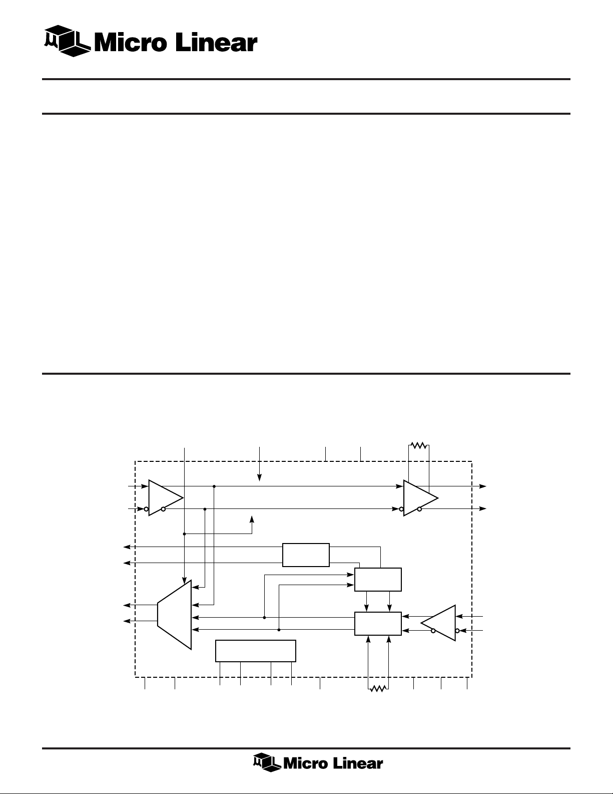
The ML6674 receive section consists of an equalizing
filter with a feedback loop for controlling effective line
compensation. The feedback loop contains a filter and
detection block for determining the proper control signal.
An ECL 100K compatible buffer at the output interfaces
directly with ATM physical interface chips.
The ML6674 transmit section accepts ECL 100K
compatible NRZ inputs.
BLOCK DIAGRAM
FEATURES
■ Complies with ATM F orum 155Mbps twisted pair
specification
■ Integrated baseline wander correction circuit
■ Integrated adaptive equalization
■ Transmitter can be externally turned off
(high impedence) for true quiet line
■ Operates over 100 meters of STP or category 5 UTP
Twisted Pair Cable
■ 32-pin PLCC and TQFP
TXIN+
TXIN–
SD+
SD–
RXOUT+
RXOUT–
LPBK TXOFF TVCCA TVCCD
LINK
STATUS
MUX
ADAPTIVE
CONTROL REFERENCE
RGNDTGNDDTGNDA
RTSET1 RTSET2
ADAPTIVE
CONTROL
ADAPTIVE
EQUALIZER
RRSET2RRSET1
RTSET
TPOUT+
TPOUT–
TPIN+
TPIN–
CMREFRVCCDRVCCARRSET
1
ML6674
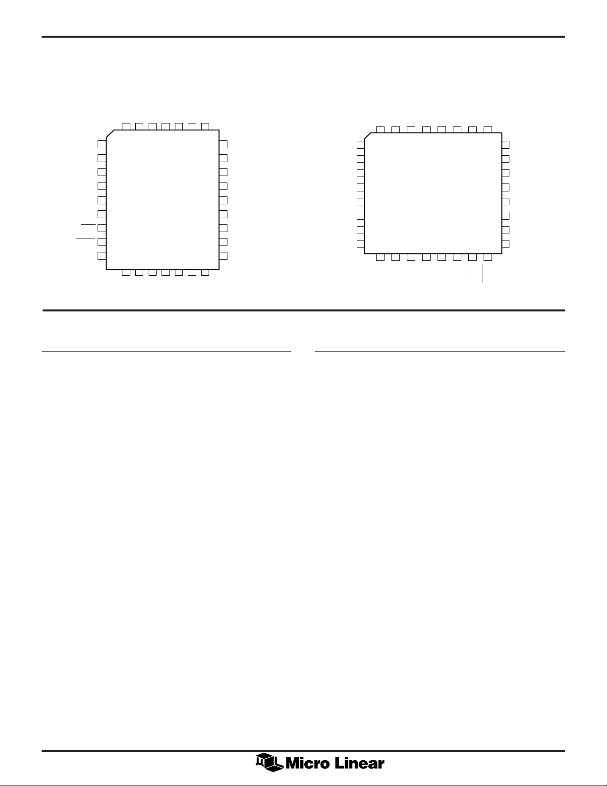
PIN CONFIGURATION
ML6674
32-Pin PCC (Q32)
RXOUT–
RVCCA
N/C
4 3 2 1 32 31 30
RXOUT+
RVCCD
TGNDD
TXOFF
SD–
SD+
N/C
LPBK
N/C
5
6
7
8
9
10
11
12
13
14 15 16 17 18 19 20
TXIN–
TXIN+
TVCCD
PIN DESCRIPTION
NAME FUNCTION
N/C
RTSET1
RTSET2
CMREF
TPOUT+
TPIN+
TPIN–
29
28
27
26
25
24
23
22
21
TPOUT–
RRSET1
RRSET2
N/C
N/C
RGND
N/C
N/C
TVCCA
TGNDA
ML6674
32-Pin TQFP (H32-7)
RRSET2
N/C
N/C
RGND
N/C
RRSET1
TPIN–
TPIN+
CMREF
N/C
N/C
RVCCA
RXOUT–
NAME FUNCTION
32 31 30 29 28 27 26 25
1
2
3
4
5
6
7
8
9 10111213141516
RVCCD
RXOUT+
SD–
SD+
N/C
N/C
TVCCA
LPBK
TGNDD
TGNDA
24
23
22
21
20
19
18
17
TXOFF
TPOUT–
TPOUT+
RTSET2
RTSET1
TVCCD
TXIN–
TXIN+
N/C
TXIN+, TXIN– These differential ECL100K compatible
inputs receive NRZ data from the PHY
for transmission.
TPOUT+, Outputs from the NRZ buffer drive
TPOUT– these differential current outputs. The
transmitter filter/transformer module
connects the media to these pins.
LPBK This TTL input enables transmitter-
Receiver loopback internally when
asserted low.
TXOFF This TTL input forces the NRZ driv er to
a high impedence state when asserted
low and shuts off transmit bias currrent.
RTSET1, An external 1% resistor connected
RTSET2 between these pins controls the
transmitter output current amplitude.
I
= 32 x 1.25V/RTSET
OUT
TVCCA, Separate analog and digital
TVCCD transmitter power supply pins help to
isolate sensitive circuitry from noise
generating digital functions. Both
supplies are nominally +5 volts.
TGNDA, Analog and digital transmitter grounds
TGNDD provide separate return paths for clean
and noisy signals.
SD+, SD– These differential ECL100K
compatible outputs indicate the
presence of a data signal with an
amplitude exceeding a preset
threshold.
TPIN+, TPIN– NRZ encoded data from the
receiver filter/transformer module
enters the Receiver through these
pins.
RXOUT+, Differential ECL100K compatible
RXOUT– outputs provide NRZ encoded data
to the PHY.
RRSET1, Internal time constants controlling
RRSET2 the equalizer’s transfer function
are set by an external resistor
connected across these pins.
CMREF This pin provides a DC common
mode reference point for the
receiver inputs.
RVCCA, Analog and digital supply pins are
RVCCD separated to isolate clean and
noisy circuit functions. Both
supplies are nominally +5 volts.
RGND Receiver ground.
2

ML6674
ABSOLUTE MAXIMUM RATINGS
Storage T emperature................................ –65°C to 150°C
Lead Temperature (Soldering, 10 sec) .....................260°C
Absolute maximum ratings are limits beyond which the
life of the integrated circuit may be impaired. All
voltages unless otherwise specified are measured with
respect to ground.
VCC Supply Voltage Range .................. GND –0.3V to 6V
Input V oltage Range
Digital Inputs..................... GND –0.3V to VCC + 0.3V
Output Current
TPOUT+/TPOUT–, SD±, RXOUT± ......................50mA
All other outputs .................................................10mA
Junction T emperature..............................................150°C
Thermal Resistance (qJA)
PLCC ............................................................... 60°C/W
TQFP ............................................................... 80°C/W
OPERATING CONDITIONS
VCC Supply Voltage.......................................... 5V ± 5%
TA, Ambient Temperature............................... 0°C to 70°C
RTSET ............................................................. 2kW ± 1%
RRSET ........................................................ 9.53kW ± 1%
Receive transformer insertion loss ..................... < –0.5dB
ELECTRICAL CHARACTERISTICS
Unless otherwise specified, TA = T
PARAMETER CONDITIONS MIN TYP MAX UNITS
DC Characteristics
Supply Current
RVCCD 74 mA
RVCCA 65 mA
TVCCD 14 mA
TVCCA 6mA
RVCCD + RVCCA + TVCCD + TVCCA 185 mA
TTL Inputs (TXOFF, LPBK)
VIL Input Low Voltage 0.8 V
VIH Input High Voltage 2.0 V
Differential Inputs (TPIN±, TXIN±)
TPIN+, TPIN–
Common Mode Input Voltage 2.2 V
TPIN+, TPIN–
Differential Input Voltage 1.5 V
TPIN+, TPIN–
Differential Input Resistance 10 kW
TPIN+, TPIN–
Common Mode Input Current +10 µA
TXIN+, TXIN–
Input Voltage HIGH (VIH)V
TXIN+, TXIN–
Input Voltage LOW (VIL)V
TXIN+, TXIN–
Input Current LOW (IIL) 0.5 µA
TXIN+, TXIN–
Input Current HIGH (IIH) 50 µA
Differential Outputs (SD±, RXOUT±, TPOUT±)
SD+, SD–, RXOUT+, RXOUT–
Output Voltage HIGH (VOH) Note 3 VCC–1.025 VCC–0.88 V
SD+, SD–, RXOUT+, RXOUT–
Output Voltage LOW (VOL) Note 3 VCC–1.81 VCC–1.62 V
TPOUT+, TPOUT–
Differential Output Current HIGH V
MIN
to T
, VCC = 5V ±5%, RTSET = 2.0ký. (Note 1)
MAX
–1.165 VCC–0.88 V
CC
–1.810 VCC–1.475 V
CC
= VCC ± 0.5, Note 2 19.0 21.0 mA
OUT
CC
V
3
 Loading...