

Micro Linear Corporation ML6622IS, ML6622CS Datasheet

Micro Linear
March 1997
ML6622*
High-Speed Data Quantizer
GENERAL DESCRIPTION
The ML6622 high-speed data quantizer (post-amplifier) is
a low noise, wide-band, BiCMOS monolithic IC designed
for high-speed signal recovery applications, such as FDDI,
Fast Ethernet, and ATM. An internal DC restoration
feedback loop nulls any offset voltage produced in the
input stage. The limiting amplifier contributes to a high
level of sensitivity and a minimum of duty cycle
distortion.
FEATURES
■ 200 MHz bandwidth
■ Low noise design
■ Adjustable Link Detect function
■ Low power design: 35mA typical
■ Used with the ML6633 LED driver
APPLICATIONS
The output of the data path is a high-speed comparator
with ECL outputs. An enable pin gates the comparator on
or off in response to the input signal level or a system
control signal.
The Link Detect circuit provides an Assert-Deassert
function with a user-selectable threshold voltage. This
circuit monitors the input signal and provides an ECL High
■ FDDI
■ Fast Ethernet, 100BASE-FX
■ ATM (SONET), 155Mbps
■ Fibre Channel, 133 or 266Mbps
■ Proprietary high-speed fiber optic data links
output within 100ms of signal acquisition and an ECL Low
output within 350ms of signal loss. The ECL discriminator
output can be used to disable the comparator when the
signal is below the user-selected threshold. LINKLED
drives an LED for a visible indication of the link status. *Some Packages Are Obsolete
BLOCK DIAGRAM
V
IN+
13
V
12
IN–
V
9
REF
GNDAVCCA
14 11 3 6
AMP
FILTER
LINK DETECT
REF
CAP THIN C
THRESH
TIMER
TIME LINKLED
CC
ECL
CMP
2161015
GNDV
LINK
OUT
4
ECL OUT+
5
ECL OUT–
1
ENABLE
7
LINK+
8
LINK–
Micro Linear
1
ML6622
PIN DESCRIPTION
PIN# NAME FUNCTION
1 ENABLE ECL input active low. When this input
is tied to LINKLED the ECL comparator
output is automatically enabled and
disabled by the Link Detect circuit.
This input can be tied to GND for
continuous enable. When the ECL
Comparator is disabled, ECL OUT–
goes low and ECL OUT+ goes high.
2 LINKLED Link Detect Status output. LINKLED is
an open collector active low signal. It
will be active low when the input
signal applied to V
IN+,VIN–
exceeds
the programmed threshold level at the
THIN pin. Capable of driving a 20mA
LED indicator.
3VCCPositive Power Supply. +5 volts
4 ECL OUT+ Positive and Negative ECL Comparator
5 ECL OUT– outputs. 1mA internal pull downs are
incorporated.
6 GND Ground connection. Used for less
noise sensitive nodes.
7 LINK+ Positive ECL Link Detect output. Active
high when the input signal exceeds the
programmed Link Detect threshold.
1mA internal pull down current
sources.
8 LINK – Negative ECL Link Detect output.
Active low when the input signal
exceeds the programmed Link Detect
threshold. 1mA internal pull down
current sources.
9V
REF
A 2.5V reference with respect to GND.
NAME PIN # FUNCTION
10 THIN Threshold Input. A voltage applied to
this input pin sets the minimum
amplitude of the input signal required
to cause the link detect to activate. In
most cases this can be tied to V
REF
11 GNDA Ground connection for noise sensitive
circuits in the chip; the input amplifier,
DC restoration loop, part of the
Comparator and part of the link detect
circuit. In some system designs, it may
be advantageous to separate GND and
GNDA.
12 V
IN–
This input pin should be capacitively
coupled to the input source or to VCCA.
13 V
IN+
This input pin should be capacitively
coupled to the input source or to VCCA.
14 VCCA Positive power supply VCC for noise
sensitive circuits as mentioned in
GNDA. +5 volts.
15 CAP A capacitor is tied from this pin to
V
. This capacitor sets the lower
REF
frequency rejection and helps remove
internal DC offset. This capacitor
should be 10 times larger than the
input capacitors.
16 C
TIMER
A capacitor from this pin to ground
determines the Link Detect response
time. To Meet FDDI specifications this
capacitor should be 2,000pF. This
capacitor can be removed for faster
response time.
.
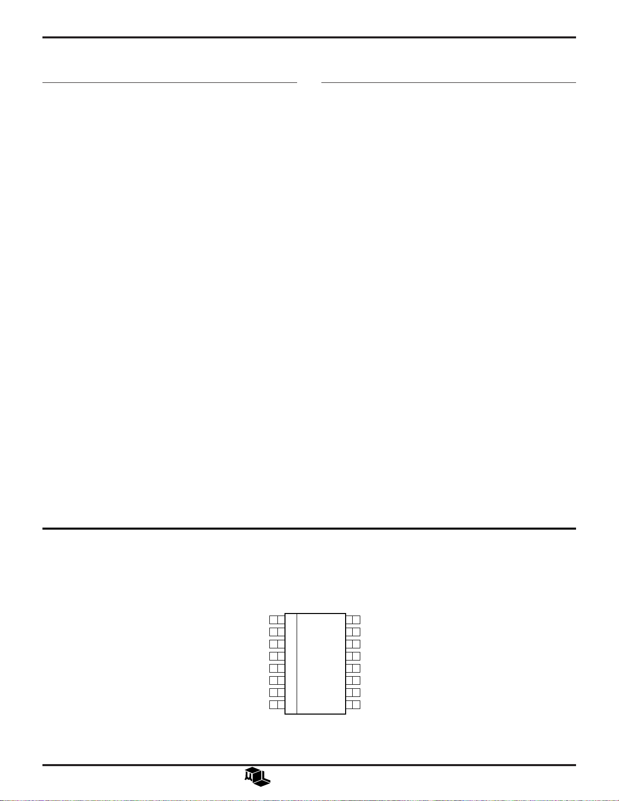
PIN CONNECTION
2
ML6622
16-Pin Narrow SOIC (S16N)
ENABLE
LINKLED
V
ECL OUT+
ECL OUT–
GND
LINK+
LINK–
CC
1
2
3
4
5
6
7
8
TOP VIEW
Micro Linear
CTIMER
16
CAP
15
V
14
13
12
11
10
9
CC
V
+
IN
V
–
IN
GNDA
THIN
V
REF
A
 Loading...