

Micro Linear Corporation ML65F16245CR, ML65F16245CT Datasheet
June 1998
PRELIMINARY
ML65F16245*
16-Bit Bidirectional Transceiver with 3-State Outputs
GENERAL DESCRIPTION
The ML65F16245 is a BiCMOS, non-inverting 16-bit
transceiver with 3-state outputs. This device was
specifically designed for high speed bus applications. Its
16 channels support propagation delay of 2ns maximum,
and fast output enable and disable times of 5ns or less to
minimize datapath delay.
This device is designed to minimize undershoot,
overshoot, and ground bounce to decrease noise delays.
These transceivers implement a unique digital and analog
implementation to eliminate the delays and noise
inherent in traditional digital designs. The device offers a
new method for quickly charging up a bus load capacitor
to minimize bus settling times, or FastBus™ Charge.
FastBus Charge is a transition current, (specified as
I
DYNAMIC
on output load) of current during the rise time and fall
time. This current is used to reduce the amount of time it
takes to charge up a heavily-capacitive loaded bus,
effectively reducing the bus settling times, and
improving data/clock margins in tight timing budgets.
Micro Linear’s solution is intended for applications for
critical bus timing designs that include minimizing
device propagation delay, bus settling time, and time
delays due to noise. Applications include; high speed
memory arrays, bus or backplane isolation, bus to bus
bridging, and sub-2ns propagation delay schemes.
) that injects between 60 to 200mA (depending
FEATURES
■ Low propagation delays — 2ns maximum for 3.3V,
2.5ns maximum for 2.7V
■ Fast output enable/disable times of 5ns maximum
■ FastBus Charge current to minimize the bus settling
time during active capacitive loading
■ 2.7V to 3.6V a V
compatible input and output levels with 3-state
capability
■ Industry standard pinout compatible to FCT, ALV, LCX,
LVT, and other low voltage logic families
■ ESD protection exceeds 2000V
■ Full output swing for increased noise margin
■ Undershoot and overshoot protection to 400mV
typically
■ Low ground bounce design
supply operation; LV-TTL
CC
The ML65F16245 follows the pinout and functionality of
the industry standard 2.7V to 3.6V-logic families.
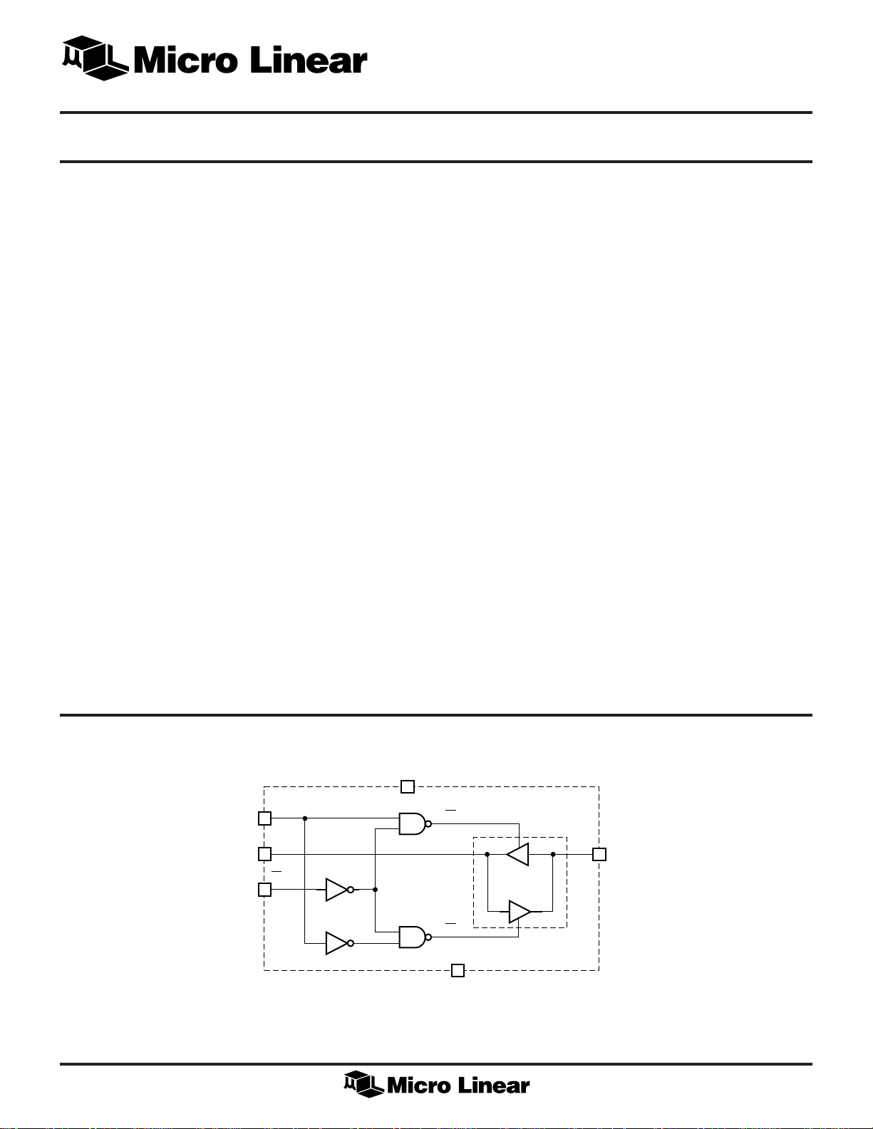
BLOCK DIAGRAM
DIR
Bi
OE
*This Part Is End Of Life As Of August 1, 2000
V
CC
OE
AB
Ai
OE
GND
Bi
BA
i=0 to 15
1
ML65F16245
PIN CONFIGURATION
1DIR
1B0
1B1
GND
1B2
1B3
V
CC
1B4
1B5
GND
1B6
1B7
2B0
2B1
GND
2B2
2B3
V
CC
2B4
2B5
GND
2B6
2B7
2DIR
ML65F16245
48-Pin SSOP (R48)
48-Pin TSSOP (T48)
1
2
3
4
5
6
7
8
9
10
11
12
13
14
15
16
17
18
19
20
21
22
23
24
48
47
46
45
44
43
42
41
40
39
38
37
36
35
34
33
32
31
30
29
28
27
26
25
1OE
1A0
1A1
GND
1A2
1A3
V
CC
1A4
1A5
GND
1A6
1A7
2A0
2A1
GND
2A2
2A3
V
CC
2A4
2A5
GND
2A6
2A7
2OE
FUNCTION TABLE
(Each 8-bit section)
OE DIR Ai Bi FUNCTION
H X Z Z Disable
L L Output Input Bus B to Bus A
L H Input Output Bus A to Bus B
L = Logic Low, H = Logic High, X = Don’t Care, Z = High Impedance
i = 0 to 7
TOP VIEW
2

PIN DESCRIPTION
ML65F16245
PIN NAME FUNCTION
1 1DIR Direction Select
2 1B0 Data Bus 1B
3 1B1 Data Bus 1B
4 GND Signal Ground
5 1B2 Data Bus 1B
6 1B3 Data Bus 1B
7V
8 1B4 Data Bus 1B
9 1B5 Data Bus 1B
10 GND Signal Ground
11 1B6 Data Bus 1B
12 1B7 Data Bus 1B
13 2B0 Data Bus 2B
14 2B1 Data Bus 2B
15 GND Signal Ground
16 2B2 Data Bus 2B
17 2B3 Data Bus 2B
18 V
19 2B4 Data Bus 2B
20 2B5 Data Bus 2B
21 GND Signal Ground
22 2B6 Data Bus 2B
23 2B7 Data Bus 2B
24 2DIR Direction Select
CC
CC
2.7V to 3.6V Supply
2.7V to 3.6V Supply
PIN NAME FUNCTION
25 2OE Output Enable
26 2A7 Data Bus 2A
27 2A6 Data Bus 2A
28 GND Signal Ground
29 2A5 Data Bus 2A
30 2A4 Data Bus 2A
31 V
32 2A3 Data Bus 2A
33 2A2 Data Bus 2A
34 GND Signal Ground
35 2A1 Data Bus 2A
36 2A0 Data Bus 2A
37 1A7 Data Bus 1A
38 1A6 Data Bus 1A
39 GND Signal Ground
40 1A5 Data Bus 1A
41 1A4 Data Bus 1A
42 V
43 1A3 Data Bus 1A
44 1A2 Data Bus 1A
45 GND Signal Ground
46 1A1 Data Bus 1A
47 1A0 Data Bus 1A
48 1OE Output Enable
CC
CC
2.7V to 3.6V Supply
2.7V to 3.6V Supply
3
 Loading...