

Micro Linear Corporation ML6599CT, ML6599CS Datasheet
February 1997
ML6599*
Hot-Insertable Active SCSI Terminator
GENERAL DESCRIPTION
The ML6599 BiCMOS 9 line SCSI terminator provides
active termination in SCSI systems using single ended
drivers and receivers. Active SCSI termination helps to
effectively control analog transmission line effects such as
ringing, noise, crosstalk, and ground bounce. In addition,
the ML6599 provides support for hot-insertability on the
SCSI bus.
The ML6599 provides a V-I characteristic optimized to
minimize transmission line effects during both signal
negation and assertion using a MOSFET-based
architecture. The desired V-I characteristic is achieved by
trimming one resistor in the control block. Internal
clamping controls signal assertion transients and provides
current sink capability to handle active negation driver
overshoots above 2.85V. It provides a 2.85V reference
through an internal low dropout (1V) linear regulator.
The ML6599 also provides a disconnect function which
effectively removes the terminator from the SCSI bus. The
disconnect mode capacitance is typically less than 5pF
FEATURES
■ Fully monolithic IC solution providing active
termination for 9 lines of the SCSI bus
■ Provides on board support for hot-insertability on the
SCSI bus
■ Low dropout voltage (1V) linear regulator, trimmed for
accurate termination current
■ Output capacitance typically < 5pF
■ Disconnect mode — logic pin to disconnect terminator
from the SCSI bus, <100µA
■ Current sinking — can sink current in excess of 10mA
per line to handle active negation driver overshoots
above 2.85V
■ Negative clamping on all lines to handle signal
assertion transients
■ Regulator can source 200mA and sink 100mA while
maintaining regulation
■ Current limit & thermal shutdown protection
per line. Current limiting and thermal shutdown
protection are also included. *Some Packages Are Obsolete
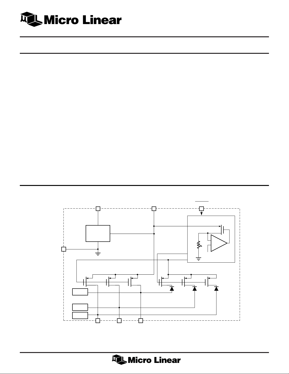
BLOCK DIAGRAM
GND
NCLAMP = Negative Clamp
NCLAMP
. . .
NCLAMP
NCLAMP
TERMPWR
LINEAR
REGULATOR
1V DROPOUT
MOSFETs WITH I
9 TERMINATION LINES
. . .
L2 L9L1
2.85V
MAX
. . .
= 24mA
R
TRIM
DISCNKT
2.85V
V
REF
CONTROL
BLOCK
V
REF
. . .
. . .
1
ML6599
PIN CONFIGURATION
20-Pin TSSOP16-Pin SOIC
TERMPWR
NC
NC
GND
DISCNKT
NC
1
2
3
4
5
6
L1
L2
7
8
16
15
14
13
12
11
10
9
L9
L8
L7
V
REF
L6
L5
L4
L3
PIN DESCRIPTION
NAME DESCRIPTION
TERMPWR Termination Power. Should be connected
to the SCSI TERMPWR line. A 10µF
tantalum local bypass capacitor is
recommended per system, as shown in
the application diagram
L1 Signal Termination 1. SCSI Bus line 1
L2 Signal Termination 2. SCSI Bus line 2
L3 Signal Termination 3. SCSI Bus line 3
L4 Signal Termination 4. SCSI Bus line 4
L5 Signal Termination 5. SCSI Bus line 5
L6 Signal Termination 6. SCSI Bus line 6
L7 Signal Termination 7. SCSI Bus line 7
L8 Signal Termination 8. SCSI Bus line 8
L9 Signal Termination 9. SCSI Bus line 9
TERMPWR
NC
GND
NC
DISCNKT
NC
HS
HS
1
2
3
4
5
6
7
8
L1
L2
9
10
20
19
18
17
16
15
14
13
12
11
L9
L8
HS
L7
V
L6
L5
L4
HS
L3
REF
NAME DESCRIPTION
V
REF
2.85V
Output. External decoupling
REF
with a 10µF tantalum in parallel with a
0.1µF ceramic capacitor is
recommended, as shown in the
application diagram.
DISCNKT Disconnect Terminator. Logic input to
disconnect the terminator from the bus
when the SCSI device no longer needs
termination due to not being the last
device on the bus or otherwise. Active
low input.
GND Ground. Signal ground (0V)
HS Heat Sink Ground. Should be
connected to GND.
NOTE : The DISCNKT line has a 200kΩ internal pullup resistor connected to the
supply. This pin should be left floating for normal operation and should
be connected to ground to enable the function.
2

ML6599
ABSOLUTE MAXIMUM RATINGS
Signal Line Voltage .................. –0.3 to TERMPWR + 0.3V
Regulator Output Current ......................... –100 to 300mA
OPERATING CONDITIONS
TERMPWR Voltage ........................................ 4V to 5.25V
Operating Temperature ................................. 0°C to 70°C
TERMPWR Voltage ........................................... –0.3 to 7V
Storage Temperature................................. –65°C to 150°C
Soldering Temperature ................................ 260°C for 10s
Thermal Impedance (θ
)
JA
SOIC ................................................................ 95°C/W
TSSOP ............................................................ 110°C/W
ELECTRICAL CHARACTERISTICS
Unless otherwise stated, these specifications apply for 4V ≤ TERMPWR ≤ 5.25V, and TA = 0°C to 70°C (Note 1)
PARAMETER CONDITIONS MIN TYP MAX UNITS
Supply
TERMPWR Supply Current L1–L9 = open, DISCNKT = open 4.5 5.5 mA
L1–L9 = 0.2 V, DISCNKT = open 225 250 mA
Disconnect Mode Current DISCNKT = 0 (active) 75 100 µA
DISCNKT
Input Low Voltage 1.0 V
Input High Voltage TERMPWR – 1.0 V
Output
Output High Voltage Measuring each signal line 2.8 2.85 2.9 V
while other eight are high
Output Current V
(Normal Mode) line while the other eight are high
Hot Insertion Peak Current TERMPWR = 0V, V
Output Clamp Level I
Sinking Current (per line) V
Output Capacitance L1 thru L9, DISCNKT = 0 4 5 pF
(Micro Linear Method) 2V
Output Capacitance L1 thru L9, DISCNKT = 0 6 7 pF
(X3T9.2/855D method) 0.4V
Regulator
Output Voltage Sourcing 0-200mA 2.8 2.85 2.9 V
Sinking Current V = 3.5V 125 150 mA
Short Circuit Current V
Dropout Voltage L1–L9 = 0.2V 1.0 1.2 V
Thermal Shutdown 170 °C
= 0.2V, Measuring each signal 20 24 mA
OUT
= 0V 1 2 µA
Any signal line (L1–L9) at 2.85V
= –30mA (Note 2) –0.15 0 0.15 V
OUT
= 3.3V (per line) 10 12 mA
OUT
100kHz square wave
P-P
applied biased at 1V D.C.
, 1MHz square wave
P-P
applied biased at 0.5V D.C.
Sinking 0-100mA 2.8 2.85 2.9 V
= 0V 150 mA
REF
V
= 5V 300 mA
REF
REF
Note 1: Limits are guaranteed by 100% testing, sampling, or correlation with worst case test conditions.
3
 Loading...