

Micro Linear Corporation ML65L245CK, ML65245CS, ML65L245CS, ML65245CK Datasheet

August 1996
ML65245**/ML65L245*
High Speed Octal Buffer Transceivers
GENERAL DESCRIPTION
The ML65245 and ML65L245 are non-inverting octal
transceivers. The high operating frequency (50MHz
driving a 50pF load) and low propagation delay
(ML65245 – 1.7ns, ML65L245 – 2ns) make them ideal for
very high speed applications such as processor bus
buffering and cache and main memory control.
These transceivers use a unique analog implementation to
eliminate the delays inherent in traditional digital designs.
Schottky clamps reduce under and overshoot, and special
output driver circuits limit ground bounce. The ML65245
and ML65L245 conform to the pinout and functionality of
the industry standard FCT245 and are intended for
applications where propagation delay is critical to the
system design.
Note: This part was previously numbered ML6580.
BLOCK DIAGRAM
FEATURES
■ Low propagation delay — 1.7ns ML65245
2.0ns ML65L245
■ Fast 8-bit TTL level transceiver with three-state
capability on the output
■ TTL compatible input and output levels
■ Schottky diode clamps on all inputs to handle
undershoot and overshoot
■ Onboard schottky diodes minimize noise
■ Reduced output swing of 0 – 4.1 volts
■ Ground bounce controlled outputs, typically less
than 400mV
■ Industry standard FCT245 type pinout
■ Applications include high speed cache memory, main
memory, processor bus buffering, and graphics cards
** This Product Is End Of Life As Of August 1, 2000
* This Product Is Obsolete
T/R
OE
V
CC
A0
20
2
V
CC
1
19
18
10
GND
B0
A1
3
17
B1
A2
16
B2
A3
4
5
15
B3
A4
6
14
B4
A5
13
B5
A6
7
8
12
B6
A7
9
11
B7
1
ML65245**/ML65L245*
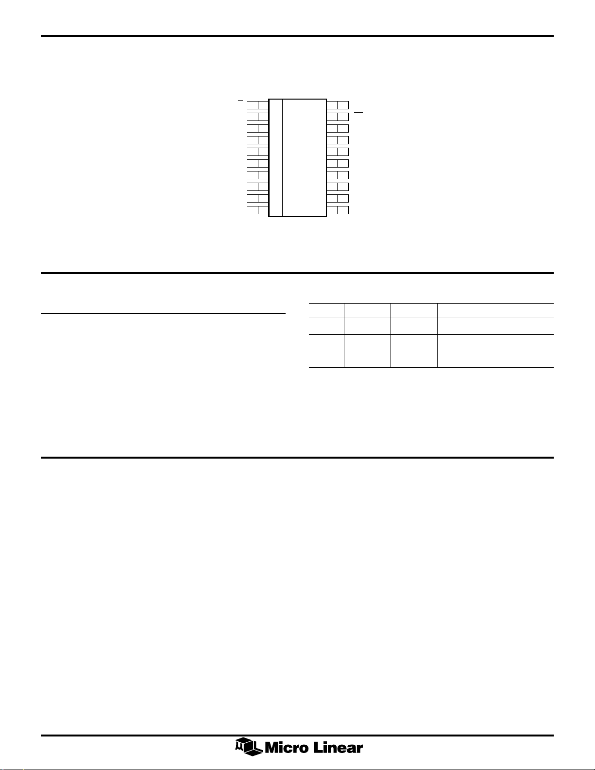
PIN CONFIGURATION
20-Pin SOIC, QSOP
PIN DESCRIPTION
NAME I/O DESCRIPTION
Ai I/O Data Bus A
Bi I/O Data Bus B
T/R I Direction select
OE I Output Enable
GND I Signal Ground
V
CC
I + 5V supply
T/R
GND
A0
A1
A2
A3
A4
A5
A6
A7
1
2
3
4
5
6
7
8
9
10
TOP VIEW
20
19
18
17
16
15
14
13
12
11
V
OE
B0
B1
B2
B3
B4
B5
B6
B7
CC
FUNCTION TABLE
OE T/R A B Function
H X Z Z Disable
L L Output Input Bus B to Bus A
L H Input Output Bus A to Bus B
L = Logic Low
H = Logic High
X = Don’t Care
Z = High Impedance
ABSOLUTE MAXIMUM RATINGS
V
................................................................................ –0.3V to 7V
CC
DC Input voltage ............................. –0.3V to VCC + 0.3V
AC Input voltage (< 20ns) ....................................... –3.0V
DC Output voltage .......................... –0.3V to VCC + 0.3V
Output sink current (per pin) ................................ 120mA
Storage temperature ................................ –65°C to 150°C
Junction temperature ............................................. 150°C
Thermal Impedance (qJA)
SOIC ...............................................................96°C/W
QSOP ............................................................ 100°C/W
2
ML65245**/ML65L245*
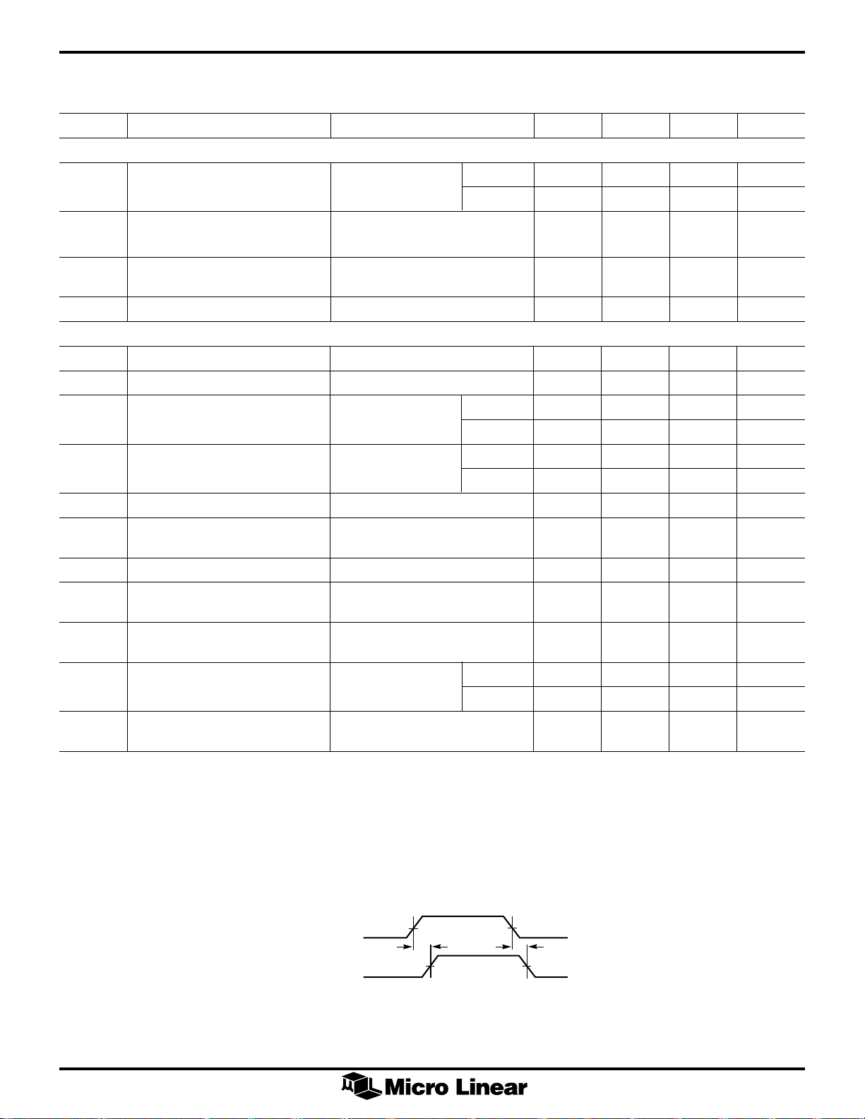
ELECTRICAL CHARACTERISTICS
Unless otherwise stated, these specifications apply for: VCC = 5.0 ± 5%V, TA = 0°C to 70°C (Note 1)
SYMBOL PARAMETER CONDITIONS MIN TYP MAX UNITS
AC ELECTRICAL CHARACTERISTICS (C
t
PLH
, t
Propagation delay Ai to/from Bi (Note 2) ML65245 1.4 1.7 ns
PHL
LOAD
= 50pF, R
LOAD
= 500ý)
ML65L245 1.6 2.0 ns
t
t
OE
OD
Output enable time 10 15 ns
OE, T/R to Ai/Bi
Output disable time 10 ns
OE, T/R to Ai/Bi
C
IN
DC ELECTRICAL CHARACTERISTICS (unless otherwise stated C
V
IH
V
I
IH
Input Capacitance 8 pF
LOAD
= 50pF, R
LOAD
= )
Input high voltage Logic HIGH 2.0 V
Input low voltage Logic LOW 0.8 V
IL
Input high current Per pin, VIN = 3V ML65245 0.5 1.5 mA
ML65L245 0.3 0.5 mA
I
IL
Input low current Per pin, VIN = 0V ML65245 2.4 3.5 mA
ML65L245 0.8 1.0 mA
I
HI-Z
Three-state output current VCC = 5.25V, 0 < V
IN
< V
CC
5µA
IOSShort circuit current VCC = 5.25V, VO = GND –60 –225 mA
(Note 3)
V
IC
V
OH
Input clamp voltage VCC = 4.75V, IIN = 18mA –0.7 –1.2 V
Output high voltage VCC = 4.75V, IOH = 100µA 2.4 V
(Notes 4 & 5)
V
OL
Output low voltage V
= 4.75V, IOL = 25mA 0.6 V
CC
(Notes 4 & 5)
V
OFF
VIN – V
per buffer VCC = 4.75V (Note 4) ML65245 0 100 200 mV
OUT
ML65L245 0 200 300 mV
I
CC
Quiescent Power VCC = 5.25V, f = 0Hz, 55 80 mA
Supply Current Inputs/outputs open
Note 1: Limits are guaranteed by 100% testing, sampling or correlation with worst case test conditions.
Note 2: One line switching, see Figure 3, t
Note 3: Not more than one output should be shorted for more than a second.
Note 4: This is a true analog buffer. In the linear region, the output tracks the input with an offset (V
Note 5: See Figure 2 for IOH versus VOH and IOL versus VOL data.
= 2.6V for the ML65245 and 2.7 for the ML65L425. V
V
IN
PLH
, t
PHL
versus CL.
INPUT
OUTPUT
OH MIN
3V
0V
3V
0V
includes V
1.5V
1.5V
. For VOL, VIN = 0V, V
OFF
OFF
1.5V
t
PLH
). For VOH, VIN = 2.7V.
tR, tF ≤ 4ns
1.5V
OL MAX
t
PHL
includes V
OFF
3
 Loading...