

Micro Linear Corporation ML6516244CR, ML6516244CT Datasheet
August 2000
PRELIMINARY
ML6516244*
16-Bit Buffer/Line Driver with 3-State Outputs
GENERAL DESCRIPTION
The ML6516244 is a BiCMOS, 16-bit buffer/line driver
with 3-state outputs. This device was specifically designed
for high speed bus applications. Its 16 channels support
propagation delay of 2.5ns maximum, and fast output
enable and disable times of 7.0ns or less to minimize
datapath delay.
This device is designed to minimize undershoot,
overshoot, and ground bounce to decrease noise delays.
These transceivers implement a unique digital and analog
implementation to eliminate the delays and noise inherent
in traditional digital designs. The device offers a new
method for quickly charging up a bus load capacitor to
minimize bus settling times, or FastBus™ Charge. FastBus
Charge is a transition current, (specified as I
DYNAMIC
injects between 60 to 200mA (depending on output load)
of current during the rise time and fall time. This current is
used to reduce the amount of time it takes to charge up a
heavily-capacitive loaded bus, effectively reducing the
bus settling times, and improving data/clock margins in
tight timing budgets.
Micro Linear’s solution is intended for applications for
critical bus timing designs that include minimizing device
propagation delay, bus settling time, and time delays due
to noise. Applications include; high speed memory arrays,
bus or backplane isolation, bus to bus bridging, and sub-
2.5ns propagation delay schemes.
The ML6516244 follows the pinout and functionality of
the industry standard 3.3V-logic families.
) that
FEATURES
■ Low propagation delays — 2.5ns maximum for 3.3V
2.25ns maximum for 5.0V
■ Fast output enable/disable times of 5.0ns maximum
■ FastBus Charge current to minimize the bus settling
time during active capacitive loading
■ 3.0 to 3.6V and 4.5 to 5.5V V
LV-TTL compatible input and output levels with 3-state
capability
■ Industry standard pinout compatible to FCT, ALV, LCX,
LVT, and other low voltage logic families
■ ESD protection exceeds 2000V
■ Full output swing for increased noise margin
■ Undershoot and overshoot protection to 400mV
typically
■ Low ground bounce design
* This part is End of Life as of August 1, 2000.
supply operation;
CC
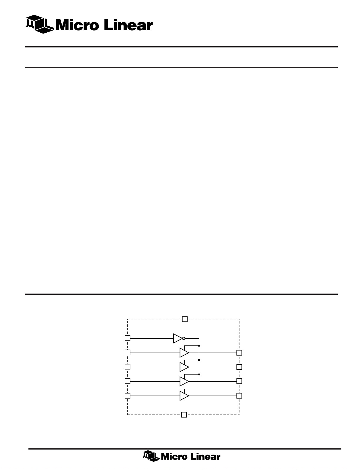
BLOCK DIAGRAM
OE
A0
A1
A2
A3
V
CC
B0
B1
B2
B3
GND
1 of 4
1
ML6516244
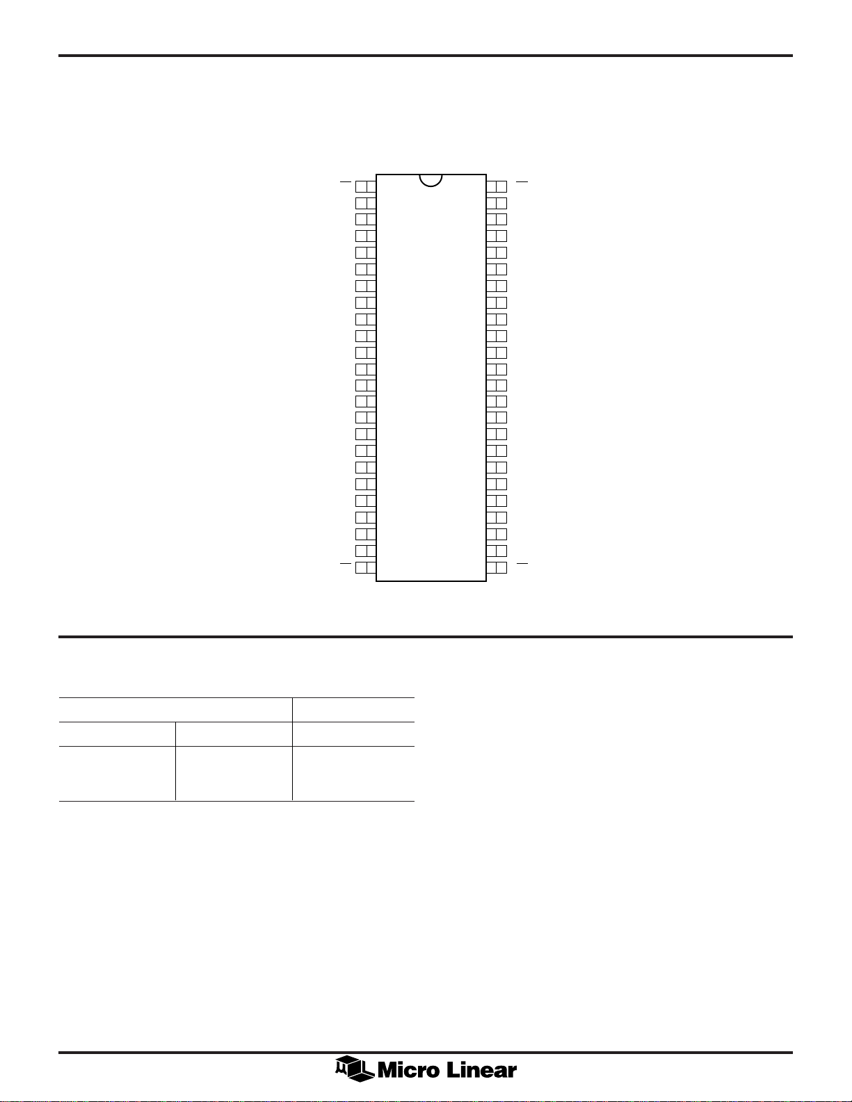
PIN CONFIGURATION
ML6516244
48-Pin SSOP (R48)
48-Pin TSSOP (T48)
1OE
1B0
1B1
GND
1B2
1B3
V
2B0
2B1
GND
2B2
2B3
3B0
3B1
GND
3B2
3B3
V
4B0
4B1
GND
4B2
4B3
4OE
CC
CC
2OE
1
2
3
4
5
6
7
8
9
10
11
12
13
14
1
15
2
16
3
17
4
18
5
19
6
20
7
21
8
22
9
23
10
24
48
1A0
47
1A1
46
GND
45
1A2
44
1A3
43
V
42
41
40
39
38
37
36
35
20
34
19
33
18
32
17
31
16
30
15
29
14
28
13
27
12
26
11
25
CC
2A0
2A1
GND
2A2
2A3
3A0
3A1
GND
3A2
3A3
V
CC
4A0
4A1
GND
4A2
4A3
3OE
FUNCTION TABLE
(Each 4-bit section)
INPUTS OUTPUTS
OE 1Ai, 2Ai, 3Ai, 4Ai 1Bi, 2Bi, 3Bi, 4Bi
LHH
LLL
HXZ
L = Logic Low, H = Logic High, X = Don’t Care, Z = High Impedance
TOP VIEW
2

PIN DESCRIPTION
ML6516244
PIN NAME FUNCTION
11OE Output Enable
2 1B0 Data Output
3 1B1 Data Output
4 GND Signal Ground
5 1B2 Data Output
6 1B3 Data Output
7V
8 2B0 Data Output
9 2B1 Data Output
10 GND Signal Ground
11 2B2 Data Output
12 2B3 Data Output
13 3B0 Data Output
CC
3.3V or 5.0V Supply
PIN NAME FUNCTION
25 3OE Output Enable
26 4A3 Data Input
27 4A2 Data Input
28 GND Signal Ground
29 4A1 Data Input
30 4A0 Data Input
31 V
32 3A3 Data Input
33 3A2 Data Input
34 GND Signal Ground
35 3A1 Data Input
36 3A0 Data Input
37 2A3 Data Input
CC
3.3V or 5.0V Supply
14 3B1 Data Output
15 GND Signal Ground
16 3B2 Data Output
17 3B3 Data Output
18 V
19 4B0 Data Output
20 4B1 Data Output
21 GND Signal Ground
22 4B2 Data Output
23 4B3 Data Output
24 4OE Output Enable
CC
3.3V or 5.0V Supply
38 2A2 Data Input
39 GND Signal Ground
40 2A1 Data Input
41 2A0 Data Input
42 V
43 1A3 Data Input
44 1A2 Data Input
45 GND Signal Ground
46 1A1 Data Input
47 1A0 Data Input
48 2OE Output Enable
CC
3.3V or 5.0V Supply
3

ML6516244
ABSOLUTE MAXIMUM RATINGS
Absolute maximum ratings are those values beyond which
the device could be permanently damaged. Absolute
maximum ratings are stress ratings only and functional
device operation is not implied.
Storage Temperature Range...................... –65°C to 150°C
Junction Temperature ............................................. 150°C
Lead Temperature (Soldering, 10sec) ...................... 150°C
Thermal Impedance (qJA) ..................................... 76°C/W
VCC............................................................................. 7V
DC Input Voltage .............................. –0.3V to VCC + 0.3V
OPERATING CONDITIONS
AC Input Voltage (PW < 20ns)................................. –3.0V
DC Output Voltage ...................................–0.3V to 7VDC
Output Current, Source or Sink ............................. 180mA
Temperature Range ........................................0°C to 70°C
VIN Operating Range ................................... 3.0V to 5.5V
ELECTRICAL CHARACTERISTICS – 3.3V OPERATION
Unless otherwise specified, VIN = 3.3V, TA = Operating Temperature Range (Note 1).
SYMBOL PARAMETER CONDITIONS MIN TYP MAX UNITS
AC ELECTRICAL CHARACTERISTICS (C
t
, t
PHL
t
OE
t
OD
T
OS
C
IN
DC ELECTRICAL CHARACTERISTICS (C
V
IH
V
IL
I
IH
I
IL
I
HI-Z
V
IC
I
DYNAMIC
Propagation Delay Ai to Bi 1.8 2.1 2.5 ns
PLH
Output Enable Time OE to Ai 7.0 ns
Output Disable Time OE to Ai 7.0 ns
Output-to-Output Skew 500 ps
Input Capacitance 5pF
Input High Voltage Logic high 2.0 V
Input Low Voltage Logic low 0.8 V
Input High Current Per pin, VIN = 3V 300 mA
Input Low Current Per pin, VIN = 0V 300 mA
Three-State Output Current VCC = 3.6V, 0 < VIN < V
Input Clamp Voltage VCC = 3.6V, IIN = 18mA –0.7 –0.2 V
Dynamic Transition Current Low to high transitions 80 mA
(FastBus Charge)
LOAD
LOAD
= 50pF)
= 50pF, R
= Open)
LOAD
CC
High to low transitions 80 mA
5 mA
V
OH
V
OL
I
CC
Note 1: Limits are guaranteed by 100% testing, sampling, or correlation with worst-case test conditions.
Output High Voltage VCC = 3.6V, IOH = –2mA 2.4 V
Output LowVoltage V
Quiescent Power Supply Current V
= 3.6V, IOL = 2mA 0.6 V
CC
= 3.6V, f = 0Hz, 3 mA
CC
inputs = VCC or 0V
4
 Loading...