

Micro Linear Corporation ML6510CQ-130, ML6510CQ-80 Datasheet
March 1997
ML6510*
Series Programmable Adaptive
Clock Manager (PACMan™)
GENERAL DESCRIPTION
The ML6510 (Super PACMan™) is a Programmable
Adaptive Clock Manager which offers an ideal solution for
managing high speed synchronous clock distribution in
next generation, high speed personal computer and
workstation system designs. It provides eight channels of
deskew buffers that adaptively compensate for clock skew
using only a single trace. The input clock can be either
TTL or PECL, selected by a bit in the control register.
Frequency multiplication or division is possible using the
M&N divider ratio, within the maximum frequency limit.
0.5X, 1X, 2X and 4X clocks can be easily realized.
The ML6510 is implemented using a low jitter PLL with
on-chip loop filter. The ML6510 deskew buffers adaptively
compensate for clock skew on PC boards. An internal
skew sense circuit is used to sense the skew caused by the
PCB trace and load delays. The sensing is done by
detecting a reflection from the load and the skew is
corrected adaptively via a unique phase control delay
circuit to provide low load-to-load skew, at the end of the
PCB traces. Additionally, the ML6510 supports PECL
reference clock outputs for use in the generation of clock
trees with minimal part-to-part skew. The chip configuration
can be programmed to generate the desired output
FEATURES
■ Input clocks can be either TTL or PECL with low
input to output clock phase error
■ 8 independent, automatically deskewed clock
outputs with up to 5ns of on-board deskew range
(10ns round trip)
■ Controlled edge rate TTL-compatible CMOS clock
outputs capable of driving 40Ω PCB traces
■ 10 to 80MHz (6510-80) or 10 to 130MHz (6510-130)
input and output clock frequency range
■ Less than 500ps skew between inputs at the
device loads
■ Small-swing reference clock outputs for minimizing
part-to-part skew
■ Frequency multiplication or division is possible using
the M&N divider ratio
■ Lock output indicates PLL and deskew buffer lock
■ Test mode operation allows PLL and deskew buffer
bypass for board debug
■ Supports industry standard processors like Pentium,™
Mips, SPARC,™ PowerPC,™ Alpha,™ etc.
frequency using the internal ROM or an external serial
EEPROM or a standard two-wire serial microprocessor
interface. *Some Packages Are Obsolete
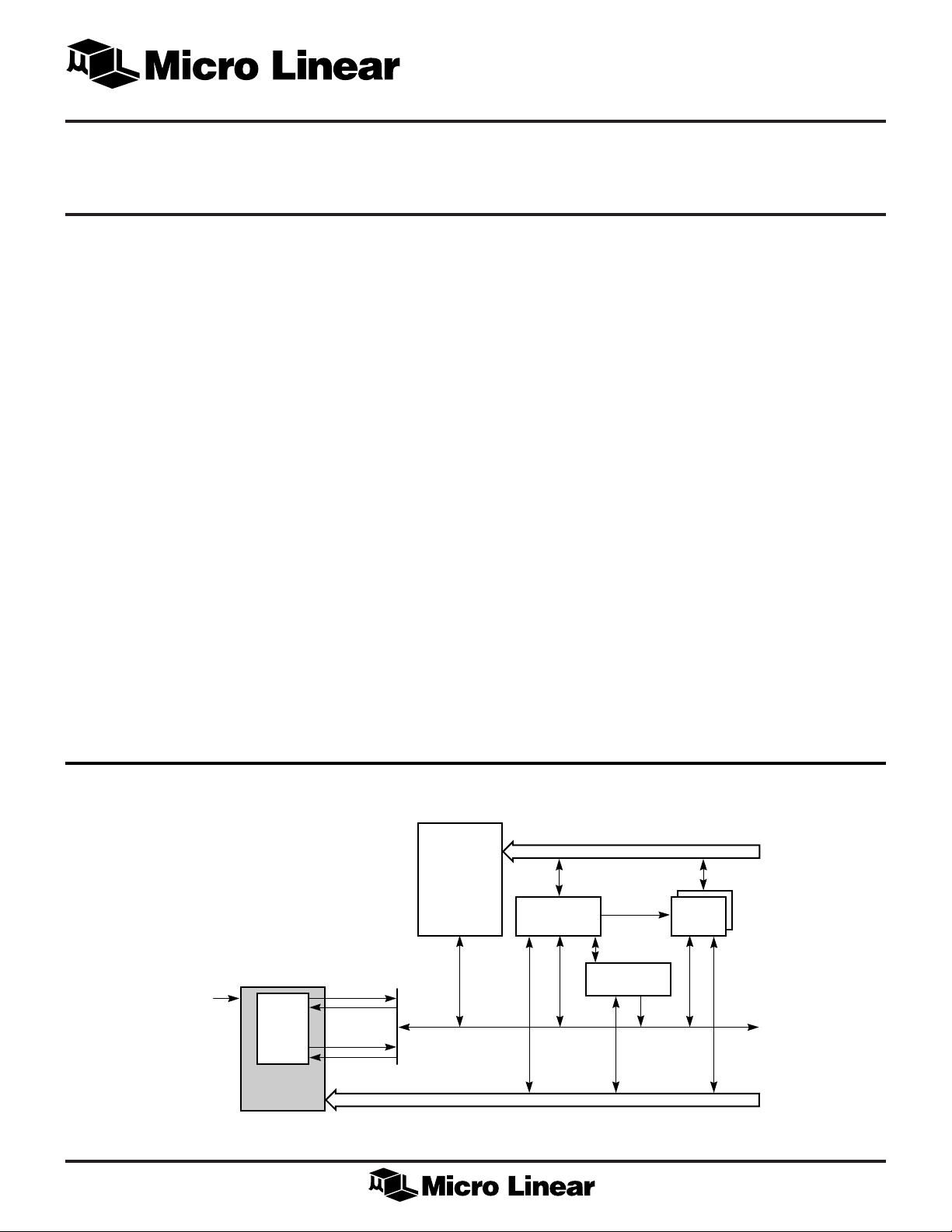
SYSTEM BLOCK DIAGRAM
CLOCK SUBSYSTEM
CLOCK IN
ML6510
LOCAL BUS
CPU
CACHE
CLK
•
8
•
•
CLOCK OUT TO
COMPONENTS
CONTROLLER
MEMORY BUS
CONTROLLER
MEMORY BUS
CACHE
RAM
1
ML6510
BLOCK DIAGRAM
CLK
INL
CLK
INH
DESKEW BUFFER 0
RESET
LOCK
MD
R0MMSB
MCLK
MD
OUT
PHASE
DETECTOR
VOLTAGE
CONTROLLED
M
PLL
N
R
MAXIMUM
DELAY
IN
MAX DELAY
CONTROL LOGIC
PROGRAMMING AND
REF
CLOCK
RCLKH RCLKL
MAX DELAY
ZERO DELAY
ZERO DELAY
DELAY
DESKEW BUFFER 1
DESKEW BUFFER 7
SENSE
CIRCUIT
DRIVE
CIRCUIT
FB0
(from remote chip)
CLK0
(to remote chip)
FB1
CLK1
FB7
CLK7
PIN CONNECTION
CLK3
DVCC23
CLK2
DGND2
FB2
FB1
DGND1
CLK1
DVCC01
CLK0
DGND0
DGND3
FB3
AGND1
AVCC1
65432
7
8
9
10
11
12
13
14
15
16
17
18 19 20 21 22
44-LEAD PLCC (Q44)
IN
FB0
MD
OUT
MD
MCLK
FB4
DGND4
CLK4
DVCC45
CLK5
DGND5
FB5
140
43
44
ML6510
TOP VIEW
23 28
25
24
LOCK
RESET
AGND3
42
26
AVCC3
41
27
RCLKL
RCLKH
39
38
37
36
35
34
33
32
31
30
29
INH
CLK
FB6
DGND6
CLK6
DVCC67
CLK7
DGND7
FB7
ROMMSB
AVCC2
AGND2
CLK
INL
2

PIN DESCRIPTION
PIN NUMBER NAME DESCRIPTION
32 ROMMSB MSB of the internal ROM address. Tie to GND if not used. See section on
ML6510
Programming the ML6510.
20 MD
19 MD
21 MCLK Programming pin. See section on Programming the ML6510.
22 RESET Reset all internal circuits. Asserted polarity is low.
23 LOCK Indicates when the PLL and deskew buffers have locked. Asserted polarity is
28 CLK
29 CLK
16,14,9,7, CLK[0–7] Clock outputs
44, 42, 37, 35
18,12,11,5, FB[0–7] Clock feedback inputs for the deskew buffers
2, 40, 39, 33
3,31 AVCC[1–3] Analog circuitry supply pins, separated from noisy digital supply pins to
25 provide isolation. All supplies are nominally +5V.
4, 30, 24 AGND[1–3] Analog circuitry ground pins
15 DVCC01 Digital supply pin for CLK0 and CLK1 output buffers. Nominally +5V.
8 DVCC23 Digital supply pin for CLK2 and CLK3 output buffers. Nominally +5V.
43 DVCC45 Digital supply pin for CLK4 and CLK5 output buffers. Nominally +5V.
OUT
IN
INH
INL
Programming pin. See section on Programming the ML6510.
Programming pin. See section on Programming the ML6510.
high.
Input clock pins. For TTL clock reference use CLK
shorted to the CLK
Input clock type is selected by the CS bit in the shift register.
pin. For PECL clock reference drive pins differentially.
INL
INH
pin
36 DVCC67 Digital supply pin for CLK6 and CLK7 output buffers. Nominally +5V.
17, 13, 10, 6, DGND[0–7] Digital ground pins for CLK [0–7] output buffers. Each clock output buffer has
1, 41, 38, 34 its own ground pin to avoid crosstalk and ground bounce problems.
26 RCLKL Differential reference clock output used to minimize
27 RCLKH part-to-part skew when building clock trees with other PACMan
integrated circuits.
3
ML6510
ABSOLUTE MAXIMUM RATINGS
VCC Supply Voltage Range ............................ –0.3V to 6V
Input Voltage Range .................................... –0.3V to VCC
Output Current
Junction Temperature .............................................. 150°C
Storage Temperature................................ –65°C to 150°C
Thermal Resistance (θJA)....................................... 54°C/W
CLK[0–7] ........................................................ 70mA
All other outputs ............................................. 10mA
ELECTRICAL CHARACTERISTICS
The following specifications apply over the recommended operating conditions of DVCC = AVCC = 5V ± 5% and ambient
temperature between 0°C and 70°C. Loading conditions are specified individually (Note 1)
SYMBOL PARAMETER CONDITIONS MIN TYP MAX UNIT
SUPPLY
DVCCXX Supply Current for each pair f
of clock outputs
IAVCC1 Static supply current, AVCC1 pin 100 120 mA
IAVCC2 Static supply current, AVCC2 pin 35 40 mA
IAVCC3 Static supply current, AVCC3 pin 1 2 mA
LOW FREQUENCY INPUTS AND OUTPUTS (ROMMSB, MD
V
IH
V
IL
V
OH
High level input voltage DVCC – 0.5 V
Low level input voltage DGND + 0.5 V
High level output voltage, IOH = –100 µA DVCC – 0.5 V
MCLK and MDIN
= 0 50 µA
CLKX
CL= 20pF, ZO = 50Ω 40 60 mA
f
= 80MHz
OUT
, MDIN, MCLK, RESET, LOCK)
OUT
V
OL
Low level output voltage, IOL = +200 µA DGND + 0.5 V
MCLK and MDIN
V
OH
High level output voltage, IOH = –100 µA 2.4 V
LOCK output IOH = –10 µA DVCC – 0.5 V
V
OL
Low level output voltage, IOL = +1 mA 0.4 V
LOCK output
I
IN
C
IN
Static input current 10 µA
Input capacitance 5 pF
HIGH FREQUENCY INPUTS AND OUTPUTS (CLK
V
IH
V
IL
V
ICM
High level input voltage CS = 0 (TTL Input Clock) 2.0 V
Low level input voltage CS = 0 (TTL Input Clock) 0.8 V
Common mode input voltage CS = 1 (PECL Input Clock) 2.0 AVCC – 0.4 V
range for PECL reference clocks
I
IH
I
IL
V
OH
V
OL
High level input current VIH = 2.4V 100 µA
Low level input current VIL = 0.4V –400 µA
High level output voltage IOH = –60mA 2.4 V
Low level output voltage IOL = +60mA 0.4 V
INH
, CLK
, FB[0-7], CLK[0-7])
INL
CS = 1 (PECL Input Clock) AVCC – 1.165 AVCC – 0.88 V
CS = 1 (PECL Input Clock) AVCC – 1.810 AVCC – 1.475 V
4
ML6510
ELECTRICAL CHARACTERISTICS (Continued)
SYMBOL PARAMETER CONDITIONS MIN TYP MAX UNIT
AC CHARACTERISTICS rise time, fall time and duty cycle are measured for a generic load; (see Load Conditions section).
t
R
t
F
f
IN
f
OUT
f
VCO
Rise time, LOAD [0-7] output 0.8 → 2.0V, 80MHz 150 1500 ps
Fall time, LOAD [0-7] output 2.0 → 0.8V, 80MHz 150 1500 ps
Input frequency, CLKIN pin 10 80 MHz
Output frequency , CLK [0-7] ML6510-80 10 80 MHz
output
ML6510-130 (Note 2) 10 130 MHz
PLL VCO operating frequency 80 160 MHz
DC Output duty cycle Measured at device load, at 1.5V 40 60 %
t
JITTER
Output jitter Cycle-to-cycle 75 ps
Peak-to-peak 150 ps
t
LOCK
PLL and deskew lock time After programming is complete 11 ms
SKEW CHARACTERISTICS All skew measurements are made at the load, at 1.5V threshold each output load can vary independently
within the specified range for a generic load (see Load Conditions section).
t
SKEWR
Output to output rising 500 ps
edge skew, all clocks
t
SKEWF
Output to output Output clock frequency ≥ 50MHz 1.5 ns
falling edge skew
t
SKEWIO
CLKIN input to any N = M = 0 600 ps
LOAD [0-7] output
rising edge skew N ≥ 2, M ≥ 2 1.25 ns
t
RANGE
t
SKEWB
Round trip delay CLKX to FBX Output frequency < 50MHz 0 10 ns
pin; output CLK period = t
CLK
Output frequency ≥ 50MHz 0 t
CLK
/2
Output-to-output rising Providing first (see LOAD 250 ps
edge skew, between matched conditions) order matching
loads order matching between outputs
PART-TO-PART SKEW CHARACTERISTICS Skew measured at the loads, at 1.5V threshold. Reference clock output pins drive clock
input pins of another ML6510.
t
PP1
Total load-to-load skew between Slave chip CS = 1, CM = 1 and 1 ns
multiple chips interfaced with N = 0, M = 0; RCLK outputs to
reference clock pins. CLKIN inputs distance less than 2"
t
PP2
Total load-to-load skew between Slave chip CS = 1, CM = 1 and 1 ns
multiple chips interfaced with N ≥ 2, M ≥ 2; RCLK outputs to
reference clock pins. CLKIN inputs distance less than 2"
PROGRAMMING TIMING CHARACTERISTICS
tRESET RESET assertion pulse 50 ns
width
t
A1
t
A2
t
A3
AUX mode MCLK high time 2000 ns
AUX mode MCLK low time 2000 ns
AUX mode MD
data 10 ns
OUT
hold time
t
A4
AUX mode MD
data 10 ns
OUT
setup time
t
A5
AUX mode MCLK period 5000 ns
5
ML6510
ELECTRICAL CHARACTERISTICS (Continued)
SYMBOL PARAMETER CONDITIONS MIN TYP MAX UNIT
PROGRAMMING TIMING CHARACTERISTICS (continued)
t
M1
t
M2
t
M3
t
M4
MAIN mode MCLK high time 900 ns
MAIN mode MCLK low time 900 ns
MAIN mode MCLK period 1800 ns
MAIN mode 900 ns
MCLK to MD
OUT
valid
(EEPROM read time)
Note 1: Limits are guaranteed by 100% testing, sampling or correlation with worst case test conditions.
Note 2: If ML6510-130 is used in a master-slave mode, the maximum operating frequency is 120MHz.
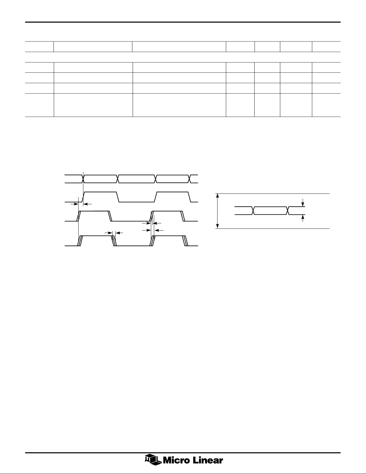
ML6510 configured with bit CM = 0:
PECL INPUT CLOCKS
OR
TTL INPUT CLOCK
LOAD [0-7]
1st Order Match
OR
t
SKEWIO
t
SKEWF
t
SKEWB
t
SKEWR
CLK
CLK
V
ICM
AVCC – 0.4V
INH
INL
2.0 V
LOAD [0-7] with
no 1st order match
Note: All skew is measured at the device load input pin, NOT at the ML6510 clock output pin. Skew is always a positive number, regardless of which edge is leading and
which is trailing.
6
 Loading...