

Micro Linear Corporation ML6509CT, ML6509CS Datasheet
February 1997
ML6509*
Active SCSI Terminator
GENERAL DESCRIPTION
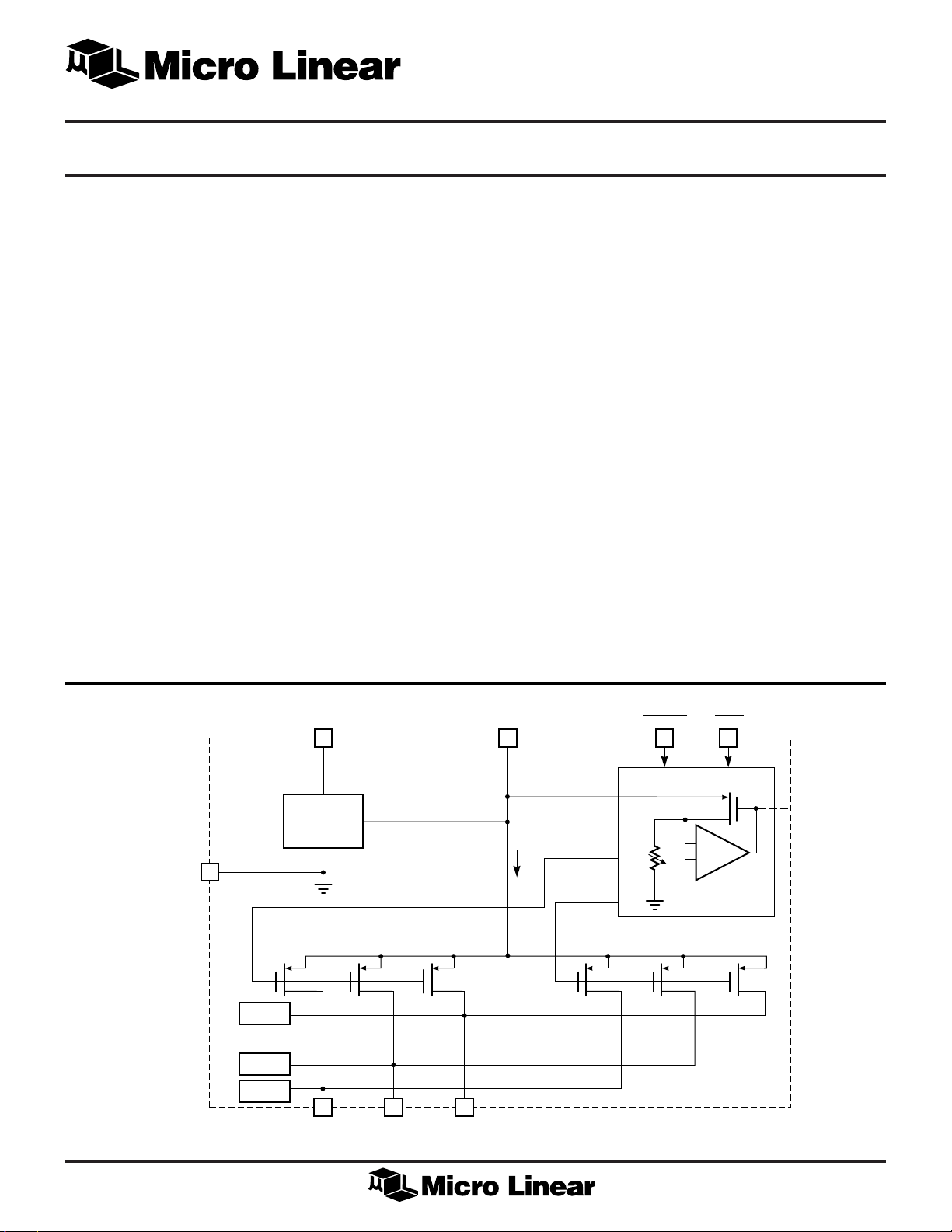
The ML6509 BiCMOS SCSI terminator provides active
termination in a SCSI system with single ended drivers and
receivers, in full compliance with the SCSI-1, SCSI-2 and
SCSI-3 recommendations. It provides a 2.85V reference
through an internal 1V dropout linear regulator. Active
SCSI termination helps the system designer to effectively
control analog transmission line effects like ringing, noise,
crosstalk, ground bounce, etc. In addition it provides
greater immunity to voltage drops on the TERMPWR line
of the SCSI bus. The desired V-I characteristics for signal
negation requires that the terminator source 0–24mA
while maintaining 2.85V and for signal assertion
preferably follow a linear slope of 110W. The ML6509
attempts to provide a V-I characteristic optimized to
minimize the transmission line effects during both signal
assertion and negation, using a MOSFET based
architecture. The desired V-I characteristic is achieved by
trimming one resistor in the control block. It provides
negative clamping for signal assertion transients and
current sink capability, to handle active negation driver
overshoots above 2.85V, which is currently accomplished
with external components in SCSI subsystems today. It
provides a disconnect mode, where the terminator is
completely disconnected from the SCSI
bus and the output capacitance is < 5pF, typically.
FEATURES
■ Fully monolithic IC solution providing active
termination for 9 lines of the SCSI bus
■ Low dropout voltage (1V) linear regulator, trimmed for
accurate termination current, with 300mA current
source capability
■ Output capacitance typically <5pF
■ Disconnect mode — logic pin to disconnect terminator
from the SCSI bus, <100µA
■ Lowpower mode — for power conscious, portable
system & peripheral applications, using less than 6"
cables. (Equivalent to a 1mA current drive with a
2.5kW termination)
■ Current sinking — can sink current >10mA per line to
handle active negation driver overshoots above 2.85V
■ Negative clamping on all lines to handle signal
assertion transients
■ Regulator can source 200mA and sink 50mA while
maintaining regulation
■ Current limit & thermal shutdown protection
■ Small and low profile package options; 16-pin SOIC
(300 mil), 20-pin TSSOP (1 mil height)
BLOCK DIAGRAM
GND
NCLAMP = Negative Clamp
NCLAMP
. . .
NCLAMP
NCLAMP
TERMPWR
LINEAR
REGULATOR
1V DROPOUT
MOSFETs WITH I
9 TERMINATION LINES
2.85V
NORMAL MODE
MAX
. . .
. . .
216mA
= 24mA
* Some Packages Are End Of Life As Of August 1, 2000
(MAX)
V
REF
MOSFETs WITH I
DISCNKT
2.85V
R
TRIM
LOW POWER MODE
V
MAX
REF
LPWR
CONTROL
BLOCK
= 1mA
. . .
1
ML6509
GENERAL DESCRIPTION (Continued)
One unique feature of the ML6509 is its support for a Low
Power mode, for use in Notebook and portable computer
applications, where it provides a 1mA (approximately
2.5KW termination) for less than 6" cable lengths. This
minimizes the battery drain significantly in such systems.
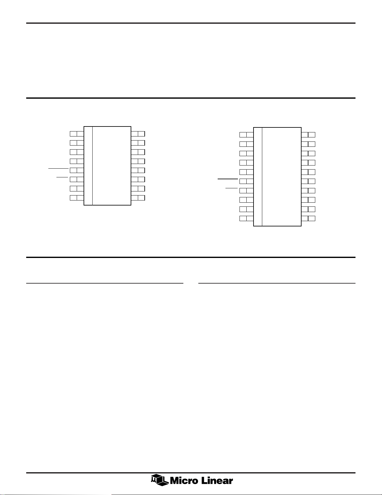
PIN CONFIGURATION
TERMPWR
GND
DISCNKT
LPWR
NC
NC
1
2
3
4
5
6
L1
L2
7
8
16
15
14
13
12
11
10
9
L9
L8
L7
V
REF
L6
L5
L4
L3
Current limiting and thermal shutdown protection are also
provided. The nine line configuration is optimal for wide
SCSI’s 18, 27, or 45 line termination needs.
20-Pin TSSOP16-Pin SOIC
TERMPWR
NC
GND
NC
DISCNKT
LPWR
HS
HS
1
2
3
4
5
6
7
8
L1
L2
9
10
20
19
18
17
16
15
14
13
12
11
L9
L8
HS
L7
V
L6
L5
L4
HS
L3
REF
PIN DESCRIPTION
NAME DESCRIPTION
TERMPWR Termination Power. Should be connected
to the SCSI TERMPWR line. A 10µF
tantalum local bypass capacitor is
recommended per system, as shown in
the application diagram
L1 Signal Termination 1. SCSI bus line 1
L2 Signal Termination 2. SCSI bus line 2
L3 Signal Termination 3. SCSI bus line 3
L4 Signal Termination 4. SCSI bus line 4
L5 Signal Termination 5. SCSI bus line 5
L6 Signal Termination 6. SCSI bus line 6
L7 Signal Termination 7. SCSI bus line 7
L8 Signal Termination 8. SCSI bus line 8
L9 Signal Termination 9. SCSI bus line 9
NOTE : The DISCNKT and LPWR lines have 200ký internal pullup resistors
connected to the supply. These pins should be left floating for normal
operation and should be connected to ground to enable the function.
NAME DESCRIPTION
V
REF
2.85V
Output. External decoupling
REF
with a 10µF tantalum in parallel with a
0.1µF ceramic capacitor is
recommended, as shown in the
application diagram.
DISCNKT Disconnect Terminator. Logic input to
disconnect the terminator from the bus
when the SCSI device no longer needs
termination due to not being the last
device on the bus or otherwise. Active
low input.
LPWR Low Power Mode. Logic input to switch
the terminator mode to a ~2.5kW
termination, with a 1mA drive capability,
meant for power conscious battery
applications which use SCSI devices
supporting cable lengths less than six
inches. Active low input.
GND Ground. Signal Ground (0V)
HS Heat Sink Ground. Should be connected
to GND.
2

ML6509
ABSOLUTE MAXIMUM RATINGS
Signal Line Voltage............................. –0.3 to TERMPWR +0.3V
Regulator Output Current ................................... –100 to 300mA
TERMPWR Voltage..................................................... –0.3 to 7V
Storage Temperature .......................................... –65°C to 150°C
Soldering Temperature ..................................... 260°C for 10 sec
Thermal Impedance (q
SOIC .......................................................................... 95°C/W
TSSOP ...................................................................... 110°C/W
)
JA
OPERATING CONDITIONS
TERMPWR Voltage.................................................. 4V to 5.25V
Operating Temperature ........................................... 0°C to 70°C
ELECTRICAL CHARACTERISTICS
Unless otherwise stated, these specifications apply for 4V - TERMPWR - 5.25V, and TA = 0°C to 70°C (Note 1)
PARAMETER CONDITIONS MIN TYP MAX UNITS
SUPPLY
TERMPWR Supply Current L1–L9 = open, DISCNKT = open 3.5 5 mA
L1–L9 = 0.2 V, DISCNKT = open 225 250 mA
DISCNKT = 0 (active) 70 100 µA
DISCNKT
Input Low Voltage LPWR, DISCNKT 1.0 V
Input High Voltage LPWR, DISCNKT TERMPWR V
–1.0
OUTPUT
Output High Voltage Measuring each signal line while 2.8 2.85 2.9 V
other eight are high
Maximum Output Current V
(Normal Mode) line while the other eight are high
Maximum Output Current V
(Lowpower Mode) measuring each signal line while the
Output Clamp Level I
Current Sink Capability V
Output Capacitance L1 thru L9, DISCNKT = 0 4 5 pF
(ML Method) 2V
Output Capacitance L1 thru L9, DISCNKT = 0 6 7 pF
(X3T9.2/855D method) 0.4V
REGULATOR
Output Voltage Sourcing 0–200mA 2.8 2.85 2.9 V
Dropout Voltage L1–L9 = 0.2V, V
Short Circuit Current Regulator output = 0V 100 mA
Thermal Shutdown 170 °C
Note 1: Limits are guaranteed by 100% testing, sampling, or correlation with worst case test conditions.
= 0.2V, Measuring each signal 20 24 mA
OUT
= 0.2V, LPWR = 0, and 0.8 1 1.2 mA
OUT
other eight are high
= –30mA –0.15 0 0.15 V
OUT
= 3.2V (per line) 7 12 mA
OUT
100kHz square wave applied
P-P
biased at 1V D.C.
, 1MHz square wave applied
P-P
biased at 0.5V D.C.
Sinking 0–50mA 2.8 2.85 2.95 V
= 2.85V 1.0 1.2 V
OUT
Regulator output = 5V 300 mA
3
 Loading...