

Micro Linear Corporation ML6440CH Datasheet
July 1999
PRELIMINARY
ML6440*
Multi-Standard 8-bit Adaptive Digital Input Comb Filter
GENERAL DESCRIPTION
The ML6440 SmartComb™ is a single-chip, 8-bit digital
comb filter that incorporates line delays and adaption
algorithms for NTSC and PAL at both CCIR601 and square
pixel rates. The ML6440 implements bandsplit filters and
a proprietary adaption and decision logic block that
allows for optimum combing over a wide range of video
sources.
The ML6440 contains all the necessary circuitry to provide
high quality combed output of luminance and
chrominance in the Y/C format. Internal filters with
integrated adaption and compensation circuits provide
filtered outputs with optimal video bandwidth and
resolution while suppressing cross-color (rainbow), crossluminance (dot crawl) and other corrupting artifacts that
can reduce video compression efficiency.
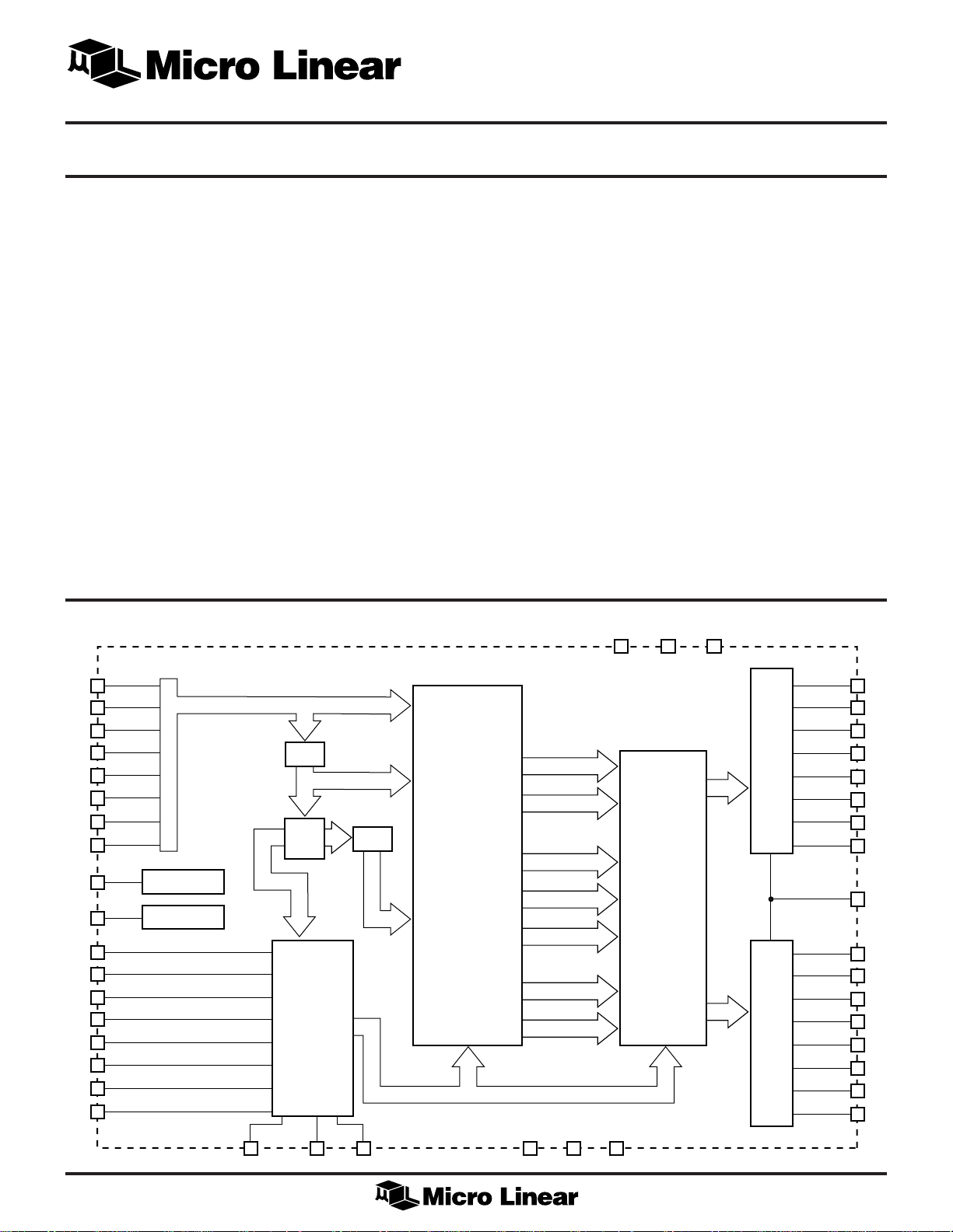
BLOCK DIAGRAM
YI0/CV0
18
19
20
21
22
23
24
25
7
6
8
9
10
11
12
13
14
15
YI1/CV1
YI2/CV2
YI3/CV3
YI4/CV4
YI5/CV5
YI6/CV6
YI7/CV7
CLK
RST
CI0/DI0
CI1/DI1
CI2/DI2
CI3/DI3
CI4/DI4
CI5/DI5
CI6/DI6
CI7/DI7
CLOCK BUFFER
DIGITAL
RESET LOGIC
PAL/NTSC MODE
CCIR601/SQ. PIXEL MODE
COMB MODE 0
COMB MODE 1
THRESHOLD CONTROL 0
THRESHOLD CONTROL 1
THRESHOLD CONTROL 2
Y+C/CV INPUT MODE
S/P
1HDL
D0
D1
D2
D3
D4
D5
D6
D7
S DATA
MUX
FILTER
AND
COMB
CONTROL
S CLK
LUMA BYPASS
1HDL
CONTROL
292826
BANDSPLIT
(NOTCH/DELAY)
FILTERS
FEATURES
■ SmartComb algorithm for automatic or manual
selection adaption thresholds
■ 3-line comb with 60+ line frame adjust
■ Comb/notch thresholds set dynamically over 60+ lines
automatically
■ 12-bit processing minimizes truncation errors and
maintains signal-to-noise performance
■ Optional 8-bit composite or separated Y/C digital inputs
■ Applications: digital TV, line doubler, imaging
■ Separate comb/notch filter thresholds for Luma and
Chroma channels
■ Optional pin controls or two-wire serial control
interface
■ Operating power dissipation less than 700mW
■ No external components, except diode and caps
* This Part Is End Of Life As Of August 1, 2000
39 16
V
CC
CC
CHROMA
BYPASS
DIGITAL
Y7
Y6
Y5
Y4
Y3
LUMINANCE
OUTPUT BUFFER
CHROMINANCE
OUTPUT BUFFER
Y2
Y1
Y0
OE
DIGITAL
C7
C6
C5
C4
C3
C2
C1
C0
30
31
32
33
34
35
36
37
27
40
41
42
43
44
1
2
3
V
HIGH BAND
LOW BAND
HIGH BAND
LOW BAND
TOTAL BAND
HIGH BAND
LOW BAND
GND GND GND
38174
5
AV
CC
SmartComb™
COMB
ADAPTION
AND
DECISION
LOGIC
1
ML6440
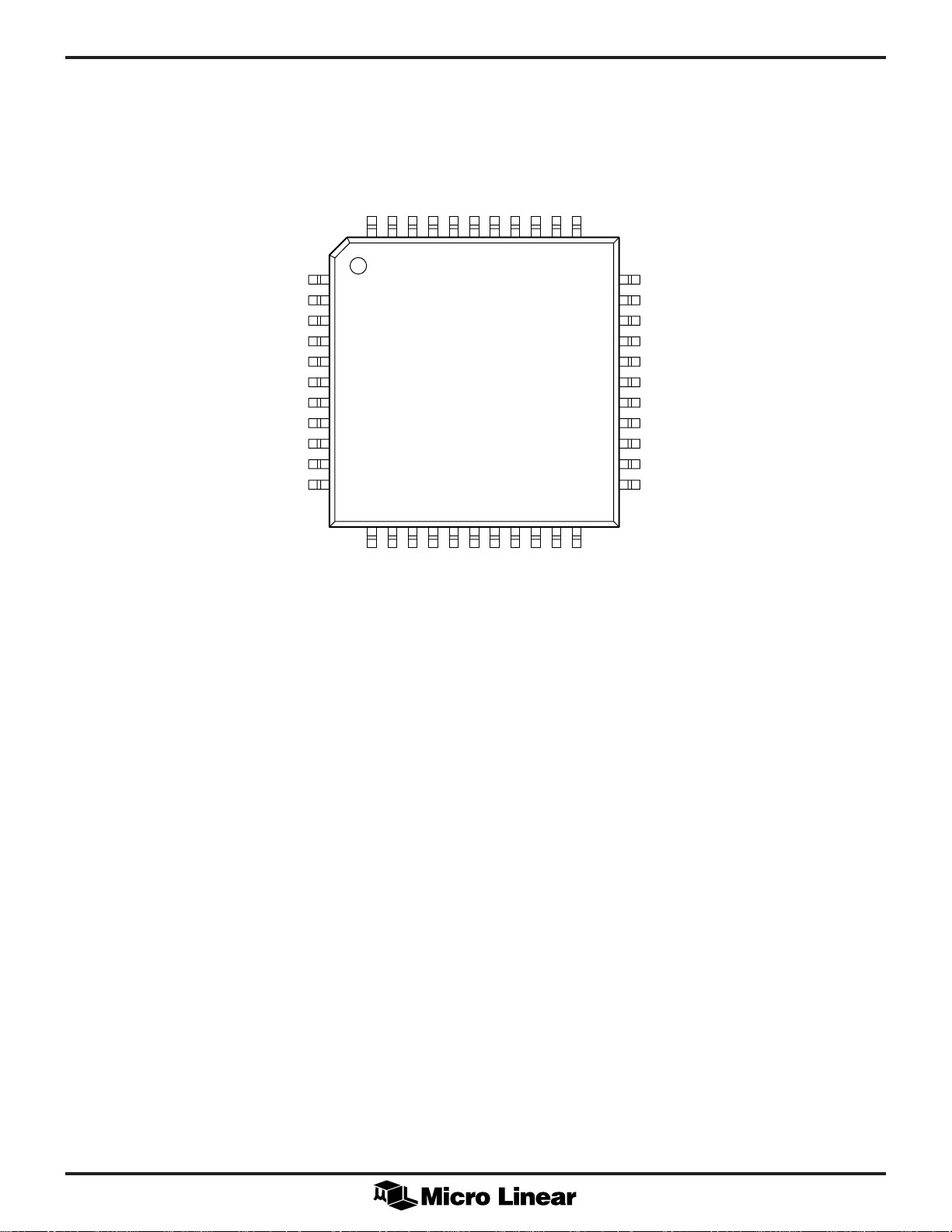
PIN CONFIGURATION
ML6440
44-Pin TQFP (H44-14)
C2
C1
C0
GND
V
CC
RST
CLK
CI0/DI0
CI1/DI1
CI2/DI2
CI3/DI3
C3C4C5C6C7
44 43 42 41 40
44 43 42 41 40
1
1
2
2
3
3
4
4
5
5
6
6
7
7
8
8
9
9
10
10
11
11
12 13 14 15 16
12 13 14 15 16 17 18 19 20 21 22
CI4/DI4
CI5/DI5
CI6/DI6
VCCGNDY0Y1Y2Y3
39 38 37 36 35 34
39 381937203621352234
17 18
CC
GND
AV
CI7/DI7
YI0/CV0
YI1/CV1
TOP VIEW
YI2/CV2
YI3/CV3
33
33
32
32
31
31
30
30
29
29
28
28
27
27
26
26
25
25
24
24
23
23
YI4/CV4
Y4
Y5
Y6
Y7
S CLK
S DATA
OE
S/P
YI7/CV7
YI6/CV6
YI5/CV5
2

PIN DESCRIPTION
ML6440
PIN NAME FUNCTION
1 C2 Chrominance output
2 C1 Chrominance output
3 C0 Chrominance output
4 GND Digital ground pin
5V
6 RST Reset input active low. Resets comb
7 CLK TTL compatible clock reference
8 CI0/DI0 (LSB) Input Chrominance signal (PAL/
9 CI1/DI1 Input Chrominance signal (Square
10 CI2/DI2 Input Chrominance signal. (Comb
11 CI3/DI3 Input Chrominance signal (Comb
CC
Digital supply pin
logic including the internal data
register. Required at power up.
NTSC control pin in control pin mode:
register bit D0)
Pixel/CCIR control pin in control pin
mode: register bit D1)
mode 0 control pin in control pin
mode: register bit D2)
mode 1 control pin in control pin
mode: register bit D3)
PIN NAME FUNCTION
20 YI2/CV2 Luma or composite video input signal
21 YI3/CV3 Luma or composite video input signal
22 YI4/CV4 Luma or composite video input signal
23 YI5/CV5 Luma or composite video input signal
24 YI6/CV6 Luma or composite video input signal
25 YI7/CV7 Luma or composite video (MSB) input
signal
26 S/P Serial/Parallel program mode. If high,
allows 8-bit parallel control using the
eight digital chrominance input pins.
Data clocks in on the positive edge
transition. If low, serial port active.
27 OE Output enable. (Y[7:0] and C[7:0]) If
low, outputs high impedance.
28 S DATA Serial data input
29 S CLK Serial clock input. Positive-edge
clocks.
30 Y7 TTL compatible luminance output
(MSB)
31 Y6 Luminance output
12 CI4/DI4 Input Chrominance signal (Adaption
Threshold 0 control pin in control pin
mode: register bit D4)
13 CI5/DI5 Input Chrominance signal (Adaption
Threshold 1 control pin mode: register
bit D5)
14 CI6/DI6 Input Chrominance signal (Adaption
Threshold 2 control pin mode: register
bit D6)
15 CI7/DI7 (MSB) Input Chrominance
(Y+C/YI control pin in control pin
mode: register bit D7)
16 AV
17 GND Ground pin for analog delay line
18 YI0/CV0 TTL compatible (LSB) Input composite
19 YI1/CV1 Luma or composite video input signal
CC
Analog supply pin. Bypass to ground
with 1µF ceramic capacitor
video signal or Y in the Y+C bypass
mode
32 Y5 Luminance output
33 Y4 Luminance output
34 Y3 Luminance output
35 Y2 Luminance output
36 Y1 Luminance output
37 Y0 Luminance output (LSB)
38 GND Digital ground pin
39 V
40 C7 TTL compatible chrominance output
41 C6 Chrominance output
42 C5 Chrominance output
43 C4 Chrominance output
44 C3 Chrominance output
CC
Digital supply pin
(LSB)
3
ML6440
ABSOLUTE MAXIMUM RATINGS
Absolute maximum ratings are those values beyond which
the device could be permanently damaged. Absolute
maximum ratings are stress ratings only and functional
device operation is not implied.
VCC............................................................................. 7V
Junction Temperature ............................................. 150°C
Storage Temperature Range...................... –65°C to 150°C
Lead Temperature (Soldering, 10 sec) ..................... 260°C
Thermal Resistance (
qJA) ...................................... 67°C/W
OPERATING CONDITIONS
Analog & Digital I/O ............. GND – 0.3V to VCC + 0.3V
Input Current .......................................................... 20µA
Temperature Range ........................................ 0°C to 70°C
VCC Range ...............................................4.75V to 5.25V
ELECTRICAL CHARACTERISTICS
Unless otherwise specified, VCC = 5V ±5%, CL = 50pF, TA = Operating Temperature Range (Notes 1, 2)
SYMBOL PARAMETER CONDITIONS MIN TYP MAX UNITS
SUPPLY
I
CC
AV
LOGIC
V
V
I
I
C
V
V
Supply Current VCC=5.25V, CLK=14.75 MHz, 60 90 mA
PAL Square Pixel
Analog Supply Voltage Recommend Operation VCC–0.6 VCC–0.4 V
CC
Low Level Input Voltage 0.8 V
IL
High Level Input Voltage V
IH
Low Level Input Current 10 µA
IL
High Level Input Current 10 µA
IH
Input Capacitance 5pF
IN
Low Level Output Voltage IOL = –2mA 0.4 V
OL
High Level Output Voltage IOH = 2mA VCC – 1.0 V
OH
Output Current 3-state Mode 10 µA
– 1.5 V
CC
C
OUT
SYSTEM TIMING
f
CLK
t
SU
Output Capacitance 3-state Mode 5 pF
CLK Input Frequency Square Pixel PAL 14.75 MHz
Setup Time to Rising CLK Edge f
Clock Low Duration f
Clock High Duration f
Input Rise Time f
Input Fall Time f
Data Valid after Rising CLK Edge f
3-state Delay Time, Output Enable f
3-state Delay Time, Output Disable f
Output Rise time f
Output Fall time f
4
Square Pixel NTSC 12.70 MHz
CCIR601 13.50 MHz
= 14.75MHz 10 ns
CLK
= 14.75MHz 30 ns
CLK
= 14.75MHz 45 ns
CLK
= 14.75MHz, 10% to 90% 20 ns
CLK
= 14.75MHz, 90% to 10% 20 ns
CLK
= 14.75MHz 20 ns
CLK
= 14.75MHz 20 ns
CLK
= 14.75MHz 20 ns
CLK
= 14.75MHz, 10% to 90% 20 ns
CLK
= 14.75MHz, 90% to 10% 20 ns
CLK
ML6440
ELECTRICAL CHARACTERISTICS (Continued)
SYMBOL PARAMETER CONDITIONS MIN TYP MAX UNITS
VIDEO SIGNAL PROCESSING
Effective Luminance Bandwidth NTSC/PAL, Comb On at –3dB (Note 3)
NTSC/CCIR601, Comb Off at –3dB 2.5 MHz
NTSC/Sq. Pixel , Comb Off at –3dB 2.5 MHz
PAL/CCIR601 , Comb Off at –3dB 2.5 MHz
PAL /Sq. Pixel, Comb Off at –3dB 2.5 MHz
Effective Chrominance Bandwidth NTSC/PAL, Comb On at –3dB (Note 3)
Centered at f
COMB FILTER CHARACTERISTICS
SNR
SNR
Signal to Noise Ratio, Chrominance Spurious Luma Artifact NTSC 48 dB
C
Signal to Noise Ratio, Luminance Spurious Subcarrier NTSC 48 dB
L
Comb Notch Depth at f
Comb Notch Bandwidth at –30dB 500 kHz
SC
SC
NTSC/CCIR601, Comb Off at –3dB 1.0 MHz
NTSC/Sq. Pixel, Comb Off at –3dB 1.0 MHz
PAL/CCIR601, Comb Off at –3dB 1.0 MHz
PAL /Sq. Pixel, Comb Off at –3dB 1.0 MHz
13.5MHz
PAL 45 dB
12.27MHz
Artifact 13.5MHz
PAL 45 dB
12.27MHz
NTSC/PAL –35 dB
5
ML6440
ELECTRICAL CHARACTERISTICS (Continued)
SYMBOL PARAMETER CONDITIONS MIN TYP MAX UNITS
SERIAL BUS LOGIC INPUT
Low Level Input Voltage 0 0.8 V
High Level Input Voltage VCC – 0.8 V
Low Level Input Current VIN = 0V 1.0 µA
High Level Input Current VIN = VCC D 1.0 µA
Input Impedance f
Input Capacitance (CIN)2pF
SYSTEM TIMING
S
CLK
Input Hysteresis (V
Spike Suppression (t
Power Setup Time to Valid Data Inputs VCC Settled to Within 1% 10 ms
Wait Time From STOP to START
On S
Hold Time for START On S
Setup Time for START On S
Min LOW Time On S
Min HIGH Time On S
Hold Time On S
Setup Time On (t
Frequency (f
(t
DATA
WAIT
CC
= 100kHz 1 M
CLK
) 100 kHz
CLOCK
) 0.2 V
HYS
) Max length for zero response 50 ns
SPIKE
) 1.3 µs
DATA (tHD/START
DATA (tSU/START
(t
CLK
LOW
(tHI) 0.6 µs
CLK
DATA (tHD/DATA
SU/DATA
) Fast mode (Note 4) 100 ns
) 1.3 µs
) 5.0 µs
) 0.6 µs
) 0.6 µs
Slow mode (Note 4) 250 ns
V
W
Rise Time for S
Fall Time for S
Setup Time for STOP On S
Note 1: Limits are guaranteed by 100% testing, sampling, or correlation with worst case test conditions.
Note 2: Supply voltage fed through 7.5W resistor to all VCC pins.
Note 3: No bandlimiting is performed on the signal bandwidth when the comb is in the “on” state.
Note 4: Parameter is luma dependent
CLK
CLK
& S
& S
DATA (tLH
DATA (tHL
DATA (tSU/STOP
) 30 300 ns
) 30 300 ns
) 0.6 µs
6
 Loading...