

Micro Linear Corporation ML6424-1, ML6424-2, ML6425-1, ML6425-2 Datasheet
February 1997
PRELIMINARY
ML6424*/ML6425*
CCIR601 Video Lowpass Filter
with Optional Sinx/x Correction
GENERAL DESCRIPTION
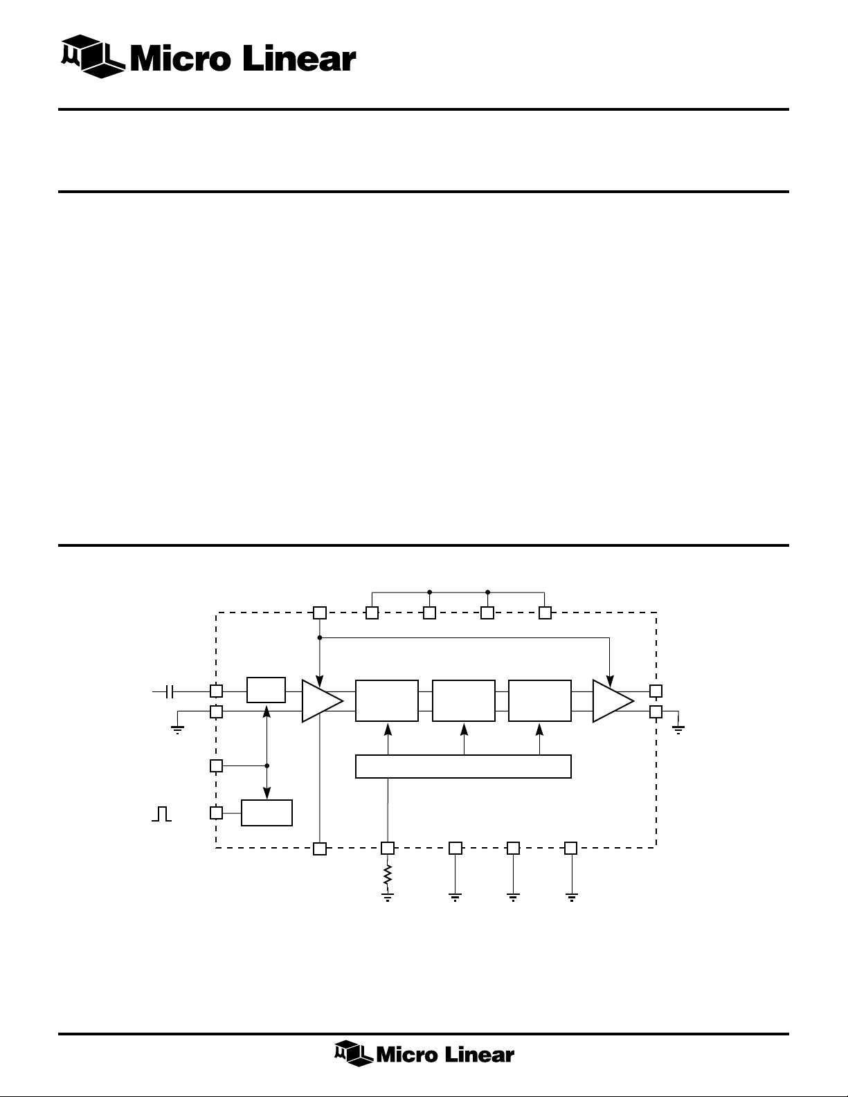
The ML6424 is a monolithic BiCMOS Video Lowpass
Filter IC, incorporating a 5th order Elliptic (Cauer) lowpass
filter, a third order allpass filter, and a 75Ω coax cable
driver. The ML6425 additionally provides sinx/x amplitude
correction. These active lowpass filters are available with
a 2.75MHz (-2) or a 5.50MHz (-1) cutoff frequency.
The input signal can be either AC or DC coupled under
the control of the MODE pin. In the DC coupled case, a
control pin (RANGE) is provided to allow the inputs to
swing down to ground. Internal self clamping is provided
for AC coupled signals.
The ML6424 and ML6425 are powered by a single 5V
supply, and can drive 1VPP into 75Ω (0.5V to 1.5V), or
2VPP into 150Ω (0.5 to 2.5V). The maximum output swing
from 0.5V to 2.5V allows easy interface to the ML6400
FEATURES
■ External or internal input clamping with pulse output
for synchronous clamping of multiple filters
■ Frequenc y tunable with R
■ ±0.25dB ripple
■ >40dB attenuation at f > 1.45 x f
■ >35dB attenuation at f > 1.45 x f
■ –12dB attenuation at f = 1.23 x f
■ Group delay distortion: ±20ns up to 0.9 x f
■ <1% peak overshoot and ringing on 2T test pulse
■ 0.5% diff. gain and 0.5⋅ diff. phase typical
■ THD <1% at 3.58 or 4.43MHz
■ Programmable input-output gain of 1x or 2x
■ 5V ±5% operation
EXT
: ±10%
(w/o sinx/x)
C
(with sinx/x)
C
C
C
family of A/D converters. *Some packages Are Obsolete
BLOCK DIAGRAM
+5V
GAIN
13
V
CC
5 11 3 1
V
CC
V
CC
V
CC
6
12
4
INPUT
CLAMP
PULSE
CONTROL
+
–
8
RANGE
5TH ORDER
LOW PASS
9 10 14 2
R
10kΩ
1%
EXT
3RD ORDER
ALL PASS
FILTER BIAS
GND GND GND
SINX/X
15
+
BUFBUF
–
V
OUT
V
OUT
167
V
IN
V
M
IN
MODE
PULSE
I/O
P
ML6424-1 ML6424-2 ML6425-1 ML6425-2
Bandwidth 5.50MHz 2.75MHz 5.50MHz 2.75MHz
Sinx/x No No Yes Yes
P
M
1
ML6424/ML6425
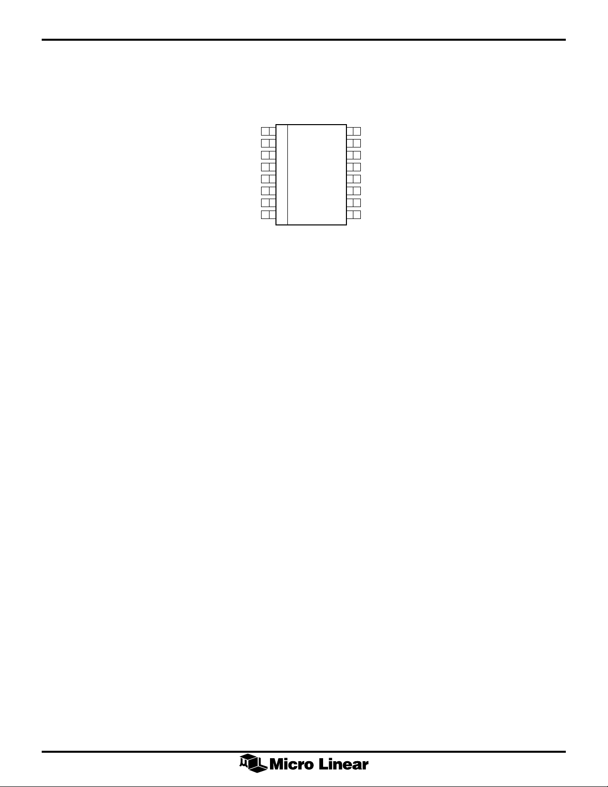
PIN CONFIGURATION
Package: S16W
16-Pin SOIC
V
GND
V
PULSE I/O
V
VIN P
V
IN
RANGE
CC
CC
CC
M
1
2
3
4
5
6
7
8
TOP VIEW
16
V
M
OUT
15
V
P
OUT
14
GND
13
GAIN
12
MODE
11
V
CC
10
GND
9
R
EXT
2
PIN DESCRIPTION
ML6424/ML6425
Pin # Name Description
1,3, V
CC
Positive supply voltages
5,11 (4.75V to 5.25V).
2,10, GND Ground voltages.
14
4 PULSE I/O U/V clamp switch control input/output
pin. When MODE is low, U/V clamp
control pulse can be applied to this
input pin. When MODE is high, the
internal circuit generates a U/V clamp
control signal to produce an output
pulse at this pin. When MODE is
floating, do not apply any voltage to
this pin since it is internally tied low in
this case. (See table below)
6,7 VIN P, Input to the filter. The input voltage for
VIN M the filter is applied to VIN P pin with
respect to VIN M pin which is
grounded. (With no connection to
MODE pin, input signal range should
be from VIN = 0.5V to 1.5V when
RANGE = Low, VIN = 0V to 1V when
RANGE = High). There is a 100µA
internal current source connected to
each of these inputs.
8 RANGE Input signal range control when
MODE is floating. When RANGE is
low, the input signal range is 0.5V to
1.5V, when RANGE is tied high the
input signal range is 0V to 1V.
9R
EXT
Precision resistor to ground that
defines the cutoff frequency of the
filter . (Typical value = 10kΩ)
10% change in R
produces a 10%
EXT
change in fC (Fig. 28).
Pin # Name Description
12 MODE Input coupling mode control pin.
When MODE is low, U/V signal can
be applied through an external ac
coupling capacitor to V
P. When
IN
MODE is high, Y signal can be applied
through an external AC coupling
capacitor to VIN P. In this case, an
internal circuitry clamps the sinc tip of
the video input signal. When MODE is
set to mid supply or left floating, input
signal can be directly applied to the
input without an A C coupling capacitor.
13 GAIN Three state gain control pin. GAIN tied
low sets the input amplifier gain to 3/4
(0.75) and the output amplifier gain to
4/3 (1.333). When GAIN is tied high,
the input amplifier gain is 3/2 (1.5) and
the output amplifier gain is 4/3. When
GAIN is set to mid supply or left to
float, the input amplifier gain is 3/4
and the output gain is 8/3 (2.666).
(See table below)
15,16 V
P, The output from the filter is derived
OUT
V
M from the V
OUT
the V
OUT
P pin with respect to
OUT
M pin which is grounded
typically. It can drive 1VPP/75Ω (0.5V
to 1.5V) or 2VPP/150Ω (0.5V to 2.5V).
If the ouput common-mode level
needs to be increased, it can be done
by raising the potential of V
OUT
M. In
this case, the output is measured from
V
P with respect to GND.
OUT
MODE INPUT COUPLING PULSE
Low AC for U/V Input
Float DC Internally biased
High AC for Y Output
Pulse Mode Table
GAIN INPUT INPUT OUTPUT OUTPUT OPTIMIZES
SELECT BUFFER BUFFER
GAIN GAIN
Low 1V
Float 1V
High 1V
0.75 1.333 1V
PP
0.75 2.666 2V
PP
1.50 1.333 2V
PP
PP
PP
PP
—
Differential
Phase
& Gain
Noise
Gain Table
3
ML6424/ML6425
ABSOLUTE MAXIMUM RATINGS
Absolute maximum ratings are those values beyond which
the device could be permanently damaged. Absolute
OPERATING CONDITIONS
Operating temperature range.........................0°C to 70⋅C
Operating supply range .......................................5V ±5%
maximum ratings are stress ratings only and functional
device operation is not implied.
DC Supply Voltage ........................................–0.3V to 7V
Analog & Digital
Inputs/Outputs................................. –0.3V to VCC + 0.3V
Input current per pin .............................. –25mA to 25mA
Storage Temperature ................................ –65°C to 150⋅C
Maximum Junction Temperature ............................ 15 0⋅C
ELECTRICAL CHARACTERISTICS
Unless otherwise specified, VCC = 4.75 to 5.25V, TA = Operating Temperature Range (Note 1).
PARAMETER CONDITIONS MIN TYP MAX UNITS
Supply Current 100 150 mA
Input Current (VIN P, VIN M) Sourcing out of the device 80 100 120 µA
Input Current Matching Between VIN P and VIN M (tied to GND) 3.0 5 %
Low Frequency Gain VIN = 100mV
Passband Ripple 100Hz < fIN < f
Differential Gain (RANGE = High) VIN: 1.0V ± 0.5V, @ 3.58 or 4.43MHz 0.5 1 %
@ 100kHz –0.2 0.0 0.2 dB
P–P
C
–0.25 0.25 dB
Differential Phase (RANGE = High) VIN: 1.0V ± 0.5V, @ 3.58 or 4.43MHz 0.5 1 Degree
Dynamic Input Signal Range (MODE = Float) RANGE = Low 0.5 1.5 V
RANGE = High 0 1 V
Output Noise (GAIN = High) Bw: 30MHz, ML6424-1 1.7 2.3 mV
Bw: 30MHz, ML6424-2 1.3 1.9 mV
Bw: 30MHz, ML6425-1 1.7 2.3 mV
Bw: 30MHz, ML6425-2 1.3 1.9 mV
Corner Frequency (fC) (±0.25dB) ML6424-1 or ML6425-1 5.23 5.50 5.78 MHz
ML6424-2 or ML6424-2 2.61 2.75 2.89 MHz
Stopband Loss (ML6424-1, -2) f
Stopband Loss (ML6425-1, -2) f
Peak Overshoot and Ringing 2T, 0.7V
Composite Chroma/Luma Delay TD(subcarrier) – TD(0); fC = 5.5MHz 20 ns
Output Short Circuit Current V
Load Capacitance V
Logic Input Low (VIL) RANGE 0.8 V
Logic Input High (VIH) RANGE VCC – 0.8 V
> 1.45 x corner frequency 35 38 dB
IN
> 1.45 x corner frequency 30 33 dB
IN
pulse 1 %
P–P
P to GND while V
OUT
P to GND 35 pF
OUT
M = GND 45 mA
OUT
RMS
RMS
RMS
RMS
Logic Input Low (IIL)V
Logic Input High (IIL)V
Note 1: Limits are guaranteed by 100% testing, sampling, or correlation with worst case conditions.
Note 2: Digital Inputs: All inputs are high impedance 1µA leakage, with MAX input voltage levels of 0.8V from each supply
= GND –1 µA
IN
= V
IN
CC
4
1µA
 Loading...