

Micro Linear Corporation ML6421CS-4, ML6421CS-5, ML6421CS-7, ML6421CS-1, ML6421CS-3 Datasheet
September 1999
ML6421*
Triple Phase and Sinx/x Equalized,
Low-Pass Video Filter
GENERAL DESCRIPTION
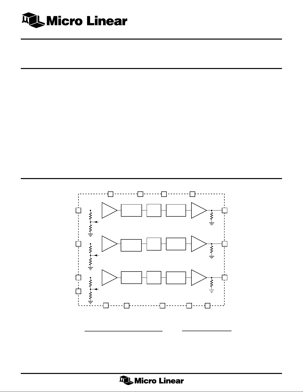
The ML6421 monolithic BiCMOS 6th-order filter provides
fixed frequency low pass filtering for video applications.
This triple phase-equalized filter with Sinx/x correction is
designed for reconstruction filtering at the output of a
Video DAC.
Cut-off frequencies are either 5.5, 8.0, or 3.0MHz. Each
FEATURES
■ 5.5, 8.0, 9.3, or 3.0MHz bandwidth
■ 1x or 2x gain
■ 6th-order filter with phase and amplitude equalizer
■ >40dB stopband rejection
■ No external components or clocks
channel incorporates a 6th-order lowpass filter, a first
order all-pass filter, a gain boost circuit, and a 75Ω coax
cable driver. A control pin (Range) is provided to allow
the inputs to swing from 0 to 1V, or 0.5 to 1.5V, by
■ ±10% frequency accuracy over maximum supply
and temperature variation
■ <2% differential gain <2° differential phase
providing a 0.5V offset to the input.
■ <25ns group delay variation
The unity gain filters are powered from a single 5V supply,
and can drive 1V
over 75Ω (0.5V to 1.5V), or 2V
P-P
P-P
over 150Ω (0.5V to 2.5V) with the internal coax drivers.
BLOCK DIAGRAM *Some Packages Are Obsolete
15
V
A
IN
3kΩ
1kΩ
I
BIAS
BUF
V
B
CC
8
LOW PASS
FILTER A
C
V
CC
6
■ Drives 1V
P-P
■ 5V ±10% operation
V
CC
5
ALL
PASS
FILTER
SINX/X
EQUALIZER
into 75Ω, or 2V
V
A
CC
11
1X/2X
BUF
3.33kΩ
into 150Ω
P-P
10
V
OUT
A
V
IN
V
IN
RANGE
B
16
3kΩ
1kΩ
2
C
3kΩ
14
1kΩ
I
I
BIAS
BIAS
BUF
BUF
12
GND
LOW PASS
FILTER B
LOW PASS
FILTER C
13
GNDA
ALL
PASS
FILTER
ALL
PASS
FILTER
4
GNDC
SINX/X
EQUALIZER
SINX/X
EQUALIZER
1
GNDB
1X/2X
BUF
1X/2X
BUF
9
3.33kΩ
7
3.33kΩ
3
GND
1x GAIN 2x GAIN
ML6221-1 ML6421-3 ML6421-4 ML6421-5 ML6421-7
FilterA 5.5MHz 8.0MHz 8.0MHz 5.5MHz 9.3MHz
Filter B 5.5MHz 8.0MHz 3.0MHz 5.5MHz 9.3MHz
Filter C 5.5MHz 8.0MHz 3.0MHz 5.5MHz 9.3MHz
Triple Input/Anti-aliasing Video Filter
V
B
OUT
C
V
OUT
1
ML6421
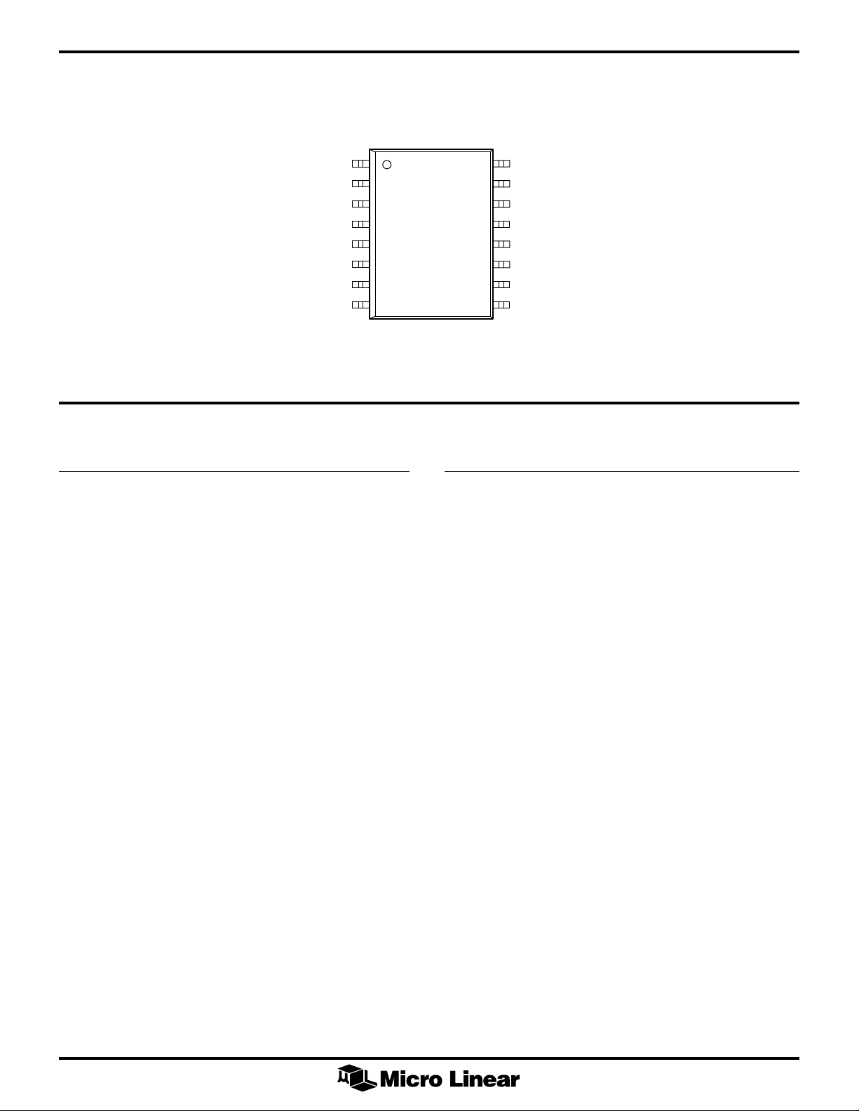
PIN CONFIGURATION
PIN DESCRIPTION
ML6421
16-Pin Wide SOIC (S16W)
CC
1
2
3
4
5
6
7
C
8
TOP VIEW
GNDB
VINC
GND
GNDC
VCCC
V
OUT
VCCB
V
16
VINB
15
VINB
14
RANGE
13
GNDA
12
GND
11
VCCA
10
V
A
OUT
9
V
A
OUT
PIN NAME FUNCTION
1 GNDB Ground pin for filter B.
2VINC Signal input to filter C. Input
impedance is 4kΩ.
3 G N D Po wer and logic ground.
4 GNDC Ground pin for filter C.
5V
CC
Positive supply.
6VCCC Power supply for filter C.
7V
C Output of filter C. Drive is 1V
OUT
75Ω (0.5V to 1.5V), or 2V
P-P
P-P
into
into
150Ω (0.5V to 2.5V).
8VCCB Power supply for filter B: 4.5V to 5.5V.
9V
B Output of filter B. Drive is 1V
OUT
75Ω (0.5V to 1.5V), or 2V
P-P
P-P
into
into
150Ω (0.5V to 2.5V).
10 V
A Output of filter A. Drive is 1V
OUT
75Ω (0.5V to 1.5V), or 2V
P-P
P-P
into
into
150Ω (0.5V to 2.5V).
PIN NAME FUNCTION
11 VCCA Power supply for filter A.
1 2 GN D Power and logic ground.
1 3 GN DA Ground pin for filter A.
14 RANGE Input signal range select.
For –1 to –4; when RANGE is low (0),
the input signal range is 0.5V to 2.5V,
with an output range of 0.5V to 2.5V.
When RANGE is high (1), the input
signal range is 0V to 2V, with an
output range of 0.5V to 2.5V.
For –5 to –7; when RANGE is low (0),
the input signal range is 0.5V to 1.5V,
with an output range of 0.5V to 2.5V.
When RANGE is high (1), the input
signal range is 0V to 1V, with an
output range of 0.5V to 2.5V.
15 VINA Signal input to filter A. Input
impedance is 4kΩ.
16 VINB Signal input to filter B. Input
impedance is 4kΩ.
2
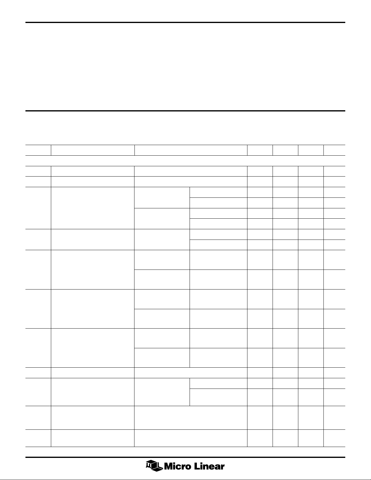
ABSOLUTE MAXIMUM RATINGS
ML6421
Absolute maximum ratings are those values beyond which
the device could be permanently damaged. Absolute
maximum ratings are stress ratings only and functional
Package Dissipation at TA = 25°C .............................. 1W
Lead Temperature (Soldering 10 sec) ......................260°C
Thermal Resistance (θJA)..................................... 65°C/W
device operation is not implied.
Supply Voltage (VCC)....................... –5.5MHz0.3 to +7V
GND .................................................. –0.3 to VCC +0.3V
OPERATING CONDITIONS
Logic Inputs ........................................–0.3 to VCC +0.3V
Input Current per Pin ............................................±25mA
Storage Temper ature.................................. –65° to 150°C
TSupply V oltage ...............................................5V ± 10%
Temperature Range ................................ 0°C < to < 70°C
ELECTRICAL CHARACTERISTICS
Unless otherwise specified VCC = 5V ± 10% and TA = T
V
= 1V
OUT
SYMBOL PARAMETER CONDITIONS MIN TYP MAX UNITS
GENERAL
R
IN
DR/R
IN
I
BIAS
for 75Ω Load (Note 1)
P-P
Input Impedance 3 4 5 kΩ
Input R Matching ±2 %
Input Current VIN = 0.5V, ML6421(–1 to –4) –80 µA
range = low ML6421(–5 to –7) 45 µA
VIN = 0.0V, ML6421(–1 to –4) –125 µA
MIN
to T
, RL =75Ω or 150Ω, V
MAX
OUT
= 2V
for 150Ω Load and
P-P
range = high ML6421(–5 to –7) –210 µA
Small Signal Gain VIN = 100mV
at 100kHz ML6421(–5 to –7) 5.5 6 6.5 dB
Differential Gain VIN = 1.1V to 2.5V ML6421(–1 to –4) 1 %
at 3.58 & 4.43 MHz
V
= 0.8V to 1.5V ML6421(–5 to –7) 1 %
IN
at 3.58 & 4.43 MHz
Differential Phase V
V
Input Range Range = 0 ML6421(–1 to –4) 0.5 2.5 V
IN
Peak Overshoot 2T, 0.7V
Crosstalk Rejection fIN = 3.58, ML6421(–1 to –4) 50 dB
= 1.1V to 2.5V ML6421(–1 to –4) 1 deg
IN
at 3.58 & 4.43 MHz
VIN = 0.8V to 1.5V ML6421(–5 to –7) 1 deg
at 3.58 & 4.43 MHz
Range = 1 ML6421(–1 to –4) 0.0 2.0 V
ML6421(-5 to -8) 0.0 1 V
fIN = 4.43MHz ML6421(–5 to –7) 45 dB
(Note 6)
P-P
pulse 2.0 %
P-P
ML6421(–1 to –4) –0.5 0 0.5 dB
ML6421(–5 to –7) 0. 5 1.5 V
Channel to Channel fIN = 100kHz ±10 ns
Group Delay Matching
(fC = 5.5MHz)
Channel to Channel fIN = 100kHz ±2 %
Group Matching
3
ML6421
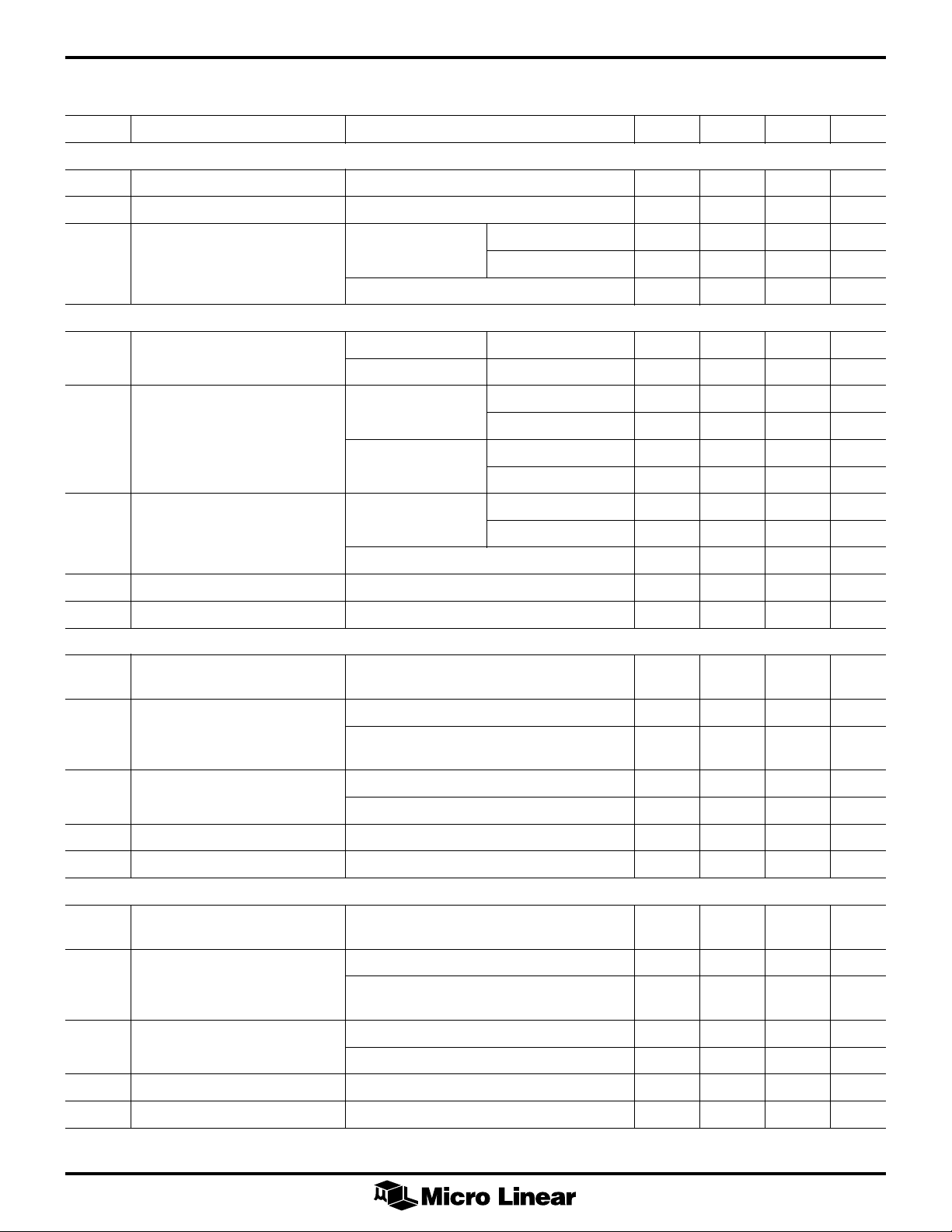
ELECTRICAL CHARACTERISTICS (Continued)
SYMBOL PARAMETER CONDITIONS MIN TYP MAX UNITS
GENERAL (Continued)
Output Current RL = 0 (short circuit) 175 mA
C
L
5.50MHZ FILTER (ML6421-1, -5)
8.0MHZ FILTER
Load Capacitance 35 pF
Composite Chroma fC = 5.5MHz ML6421(–1 to –4) ±15 ns
/Luma delay ML6421(–5 to –7) ± 15 n s
Bandwidth –0.75dB (Note 5) ML6421(–1 to –4) 4.95 5.50 6.05 MHz
(monotonic passband) –0.55dB (Note 5) ML6421(–5 to –7) 4.95 5.50 6.05 MH z
Subcarrier Frequency Gain fIN = 3.58MHz ML6421(–1 to –4) –0.3 0.2 0.7 dB
ML6421-1 ML6421(–5 to –7) –0.9 1.4 1.9 dB
Attenuation fIN = 10MHz ML6421(–1 to –4) 16 1 8 dB
Output Noise BW = 30MHz (Note 6) 1000 µV
Group Delay 145 ns
fC = 8.0MHz/9.3MHz ±8 ns
fIN = 4.43MHz ML6421(–1 to –4) –0.35 0.1 0.65 dB
ML6421(–5 to –7) 1. 1 1.6 2 .1 dB
ML6421(–5 to –7) 2 0 25 dB
fIN = 50MHz 40 45 dB
RMS
Bandwidth –3dB (Note 5) 7.2 8 8.8 MHz
(monotonic passband)
Subcarrier Frequency Gain fIN = 3.58MHz –0.25 0.25 0.75 dB
ML6421-3 or ML6421 fIN = 4.43MHz –0.11 0.39 0.89 dB
4/ML6421-7
Attenuation fIN = 17MHz 20 25 dB
Output Noise BW = 30MHz (Note 6) 1000 µV
Group Delay 120 ns
9.3MHZ FILTER
Bandwidth –2dB (Note 5) 8.4 9.3 10.2 MHz
(monotonic passband)
Subcarrier Frequency Gain fIN = 3.58MHz –0.01 0.4 0.9 dB
ML6421-3 or ML6421 fIN = 4.43MHz –0.1 0.6 1.1 dB
4/ML6421-7
Attenuation fIN = 17MHz 20 25 dB
Output Noise BW = 30MHz (Note 6) 1000 µV
Group Delay 120 ns
fIN = 85MHz 40 42 dB
RMS
fIN = 85MHz 40 42 dB
RMS
4
 Loading...