

Micro Linear Corporation ML6401CS-1, ML6401CS-3 Datasheet
March 1997
ML6401*
8-Bit 20 MSPS A/D Converter
GENERAL DESCRIPTION
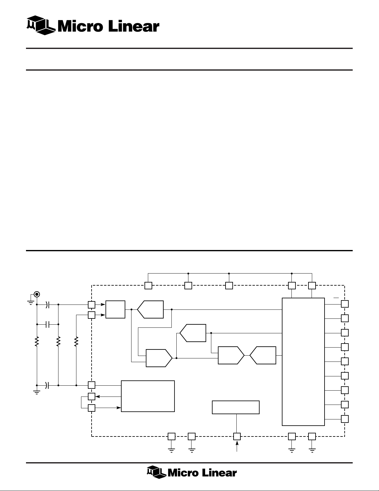
The ML6401 is a single-chip 8-bit 20 MSPS BiCMOS Video
FEATURES
■ 5.0V ±10% single supply operation
A/D Converter IC, incorporating a differential input track
and hold, clock generation circuitry, and reference voltage.
The input track and hold consists of a low (4pF)
capacitance input and a fast settling operational amplifier.
The A/D conversion is accomplished through a pipeline
approach, reducing the number of required comparators
and latches. The non-over-lapping clocks required for this
architecture are all internally generated. Clock generation
circuitry requires only one 50% duty cycle clock input.
The use of error correction throughout the A/D converter
improves DNL. All bias voltages and currents required by
the A/D converter are internally generated. The digital
outputs are three-stateable.
■ Internal reference voltage
■ Power dissipation less than 200mW typical
■ Replaces TMC1175MC20 and AD775JR,
functionally compatible to Sony CXD1175AM/AP
■ 16-pin reduced pin count packages
available: ML6401CS-3
■ Low input capacitance track and hold: 4pF
■ Onboard non-overlapping clock generation to
minimize external components
■ Three-state outputs and no missing codes
■ 150MHz input track and hold
BLOCK DIAGRAM/TYPICAL APPLICATION *Some Packages Are End Of Life
VIDEO
INPUT
75Ω
47µF
0.1µF
10µF
5V
VDD
A
+
+
VIN+
150MHz
T & H
–
V
IN
1kΩ1kΩ
VIN
-BIAS
VREF
VREF
OUT
IN
1.5V
1.0V
ADC 1
SUB
DAC
AMP
INTERNAL
REFERENCES
GND
A
VDD
ADC 2
GND
A
A
VDD
A
SUB
DAC
AMP
CLOCK GENERATOR
CLK
20MHz
ADC 3
VDD
GND
D
DIGITAL
ERROR
CORRECTION
D
VDD
GND
D
OE
D7
D6
D5
D4
D3
D2
D1
D0
O
1
ML6401
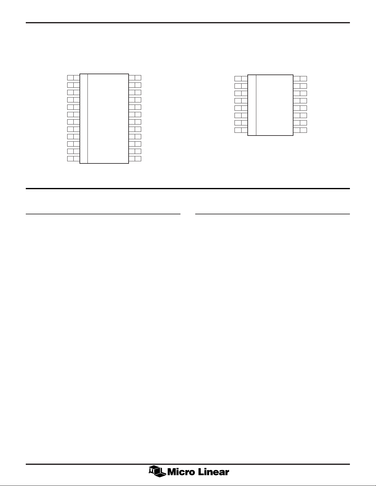
PIN CONFIGURATION
ML6401-1
24-Pin SOIC (S24W)
GND
VDD
OE
D0
D1
D2
D3
D4
D5
D6
D7
CLK
1
O
O
2
3
4
5
6
7
8
9
10
11
12
TOP VIEW
24
23
22
21
20
19
18
17
16
15
14
13
GND
VIN–
V
IN–BIAS
GNDA
GNDA
V
+
IN
VDD
VREF
VREF
VDD
VDD
VDD
D
A
IN
OUT
A
A
D
PIN DESCRIPTION (Pin numbers in parentheses are for S16N package)
PIN NAME DESCRIPTION
1 (16) OE Output Enable. A logic low signal
on this pin enables the outputs.
2 GNDOOutput ground pin.
3 (1) D0 D0 (LSB) output signal (TTL
compatible).
4 (2) D1 D1 output signal (TTL compatible).
PIN NAME DESCRIPTION
13 (9,11) VDD
14 (12) VDD
15 (12) VDD
16 VREF
D0
D1
D2
D3
D4
D5
D6
D7
ML6401-3
16-Pin SOIC (S16N)
1
2
3
4
5
6
7
8
TOP VIEW
Digital supply pin.
D
Analog supply pin.
A
Analog supply pin.
A
Full scale reference output.
OUT
16
15
14
13
12
11
10
9
Connect to pin 17 for self bias.
(VRTS on 1175) (ML401-1 only)
OE
GND
GND
VIN+
VDD
VDD
CLK
VDD
D
A
A
D
D
5 (3) D2 D2 output signal (TTL compatible).
6 (4) D3 D3 output signal (TTL compatible).
7 (5) D4 D4 output signal (TTL compatible).
8 (6) D5 D5 output signal (TTL compatible).
9 (7) D6 D6 output signal (TTL compatible).
10 (8) D7 D7 (MSB) output signal (TTL
compatible).
11 VDDOOutput supply pin.
12 (10) CLK Clock input pin.
17 VREF
Full scale reference input.
IN
Connect to pin 16 for self bias.
(VRT on 1175) (ML401-1 only)
18 (12) VDD
Analog supply pin.
A
19 (13) VIN+ Input signal.
20 (14) GND
21 (14) GND
22 V
IN–BIAS
Analog ground.
A
Analog ground.
A
Common mode bias output.
Connect to pin 23 for self bias.
(VRBS on 1175) (ML401-1 only)
23 VIN– Common mode bias input.
Connect to pin 22 for self bias.
Drive with the negative input if
differential input is being used.
(VRB on 1175)
(ML401-1 only)
24 (15) GND
Digital Ground.
D
2

ABSOLUTE MAXIMUM RATINGS
ML6401
Absolute maximum ratings are those values beyond which
the device could be permanently damaged. Absolute
maximum ratings are stress ratings only and functional
device operation is not implied.
Supply Current (ICC) ............................................... 55mA
Peak Driver Output Current ............................... ±500mA
Analog Inputs ...................................................–0.3 to 7V
Junction Temperature ............................................. 150°C
Storage Temperature Range ..................... –65°C to 150°C
Lead Temperature (soldering, 10 sec) ..................... 150°C
Thermal Resistance (θ
)
JA
Plastic DIP ....................................................... 80°C/W
Plastic SOIC ................................................... 110°C/W
OPERATING CONDITIONS
Temperature Range ....................................... 0°C to 70°C
T
PWH(min)
= T
PWL(min)
............................................... 25ns
ELECTRICAL CHARACTERISTICS
Unless otherwise specified, CL = 15pF, V
PARAMETER CONDITIONS MIN TYP MAX UNITS
Resolution 8 Bits
Power Dissipation 200 325 mW
Transfer Function
DC Integral Linearity f
DC Differential Linearity f
AC Integral Linearity V
Offset Voltage VIN– = V
Gain Error VIN– = V
Analog Signal Processing
= 5V ±10%, T
CC
= 15MSPS ±0.8 ±1.25 LSB
CLk
= 15MSPS ±0.6 ±1 LSB
CLk
= 2V, 4.4MHz ±2 LSB
IN
IN–BIAS
IN–BIAS
= Operating Temperature Range (Note 1).
A
, VREF
, VREF
OUT
OUT
= VREF
= VREF
IN
IN
±10 LSB
±2 ±5 LSB
Differential Gain V
Differential Phase V
Signal to Noise Ratio VIN = 2V, 1MHz, f
= NTSC 40 IRE modulated ramp,
IN
f
= 14.3 MSPS 1.8 %
CLK
= NTSC 40 IRE modulated ramp,
IN
f
= 14.3 MSPS 0.9 degree
CLK
= 20MHz 48 dB
CLK
Distortion 0.18 %
Spurious Free Dynamic Range 58 dB
SIN and Distortion (SINAD) 47 dB
Effective Bits 7.4 bits
Analog Inputs
Input Voltage Digital Output = 0,
VIN– = V
IN–BIAS
, VREF
OUT
= VREF
IN
0.5 V
Digital Output = 255,
Input Current f
VIN– = V
= 20MHz ±20 ±30 µA
CLK
IN–BIAS
, VREF
OUT
= VREF
IN
2.5 V
Input Capacitance VIN = 2V 4.0 pF
Analog Input Bandwidth 150 MHz
Reference Outputs
V
IN–BIAS
VREF
V
RIN
OUT
IREF
= 50µA 0.97 1.0 1.03 V
OUT
1.45 1.5 1.55 V
±5 µA
3
 Loading...