

Micro Linear Corporation ML4903CT Datasheet
July 1999
ML4903
High Current Synchronous Buck Controller
GENERAL DESCRIPTION
The ML4903 high current synchronous buc k controller
provides high efficiency DC/DC conversion to generate
V
for processors such as the Pentium® Pro and Pentium
CCP
II from Intel
®
.
The ML4903 controller, when combined with two external
MOSFETs, generates output voltages between 1.8V and
3.5V from a 12V supply. The output voltage is selected via
an internal 2 chord 4-bit DAC. In the upper range, the
output can be set between 2.1V and 3.5V in 100mV steps.
In the lower range, the output can be set between 1.8V
and 2.05V in 50mV steps. Output currents in excess of
20A can be attained at efficiencies greater than 80%.
The ML4903 can be enabled/disabled via the SHDN pin.
While disabled, the output of the regulator is completely
isolated from the circuit’s input supply. The ML4903
employs fixed-frequency PWM control combined with a
sophisticated control loop enhancement circuit to provide
excellent load transient response.
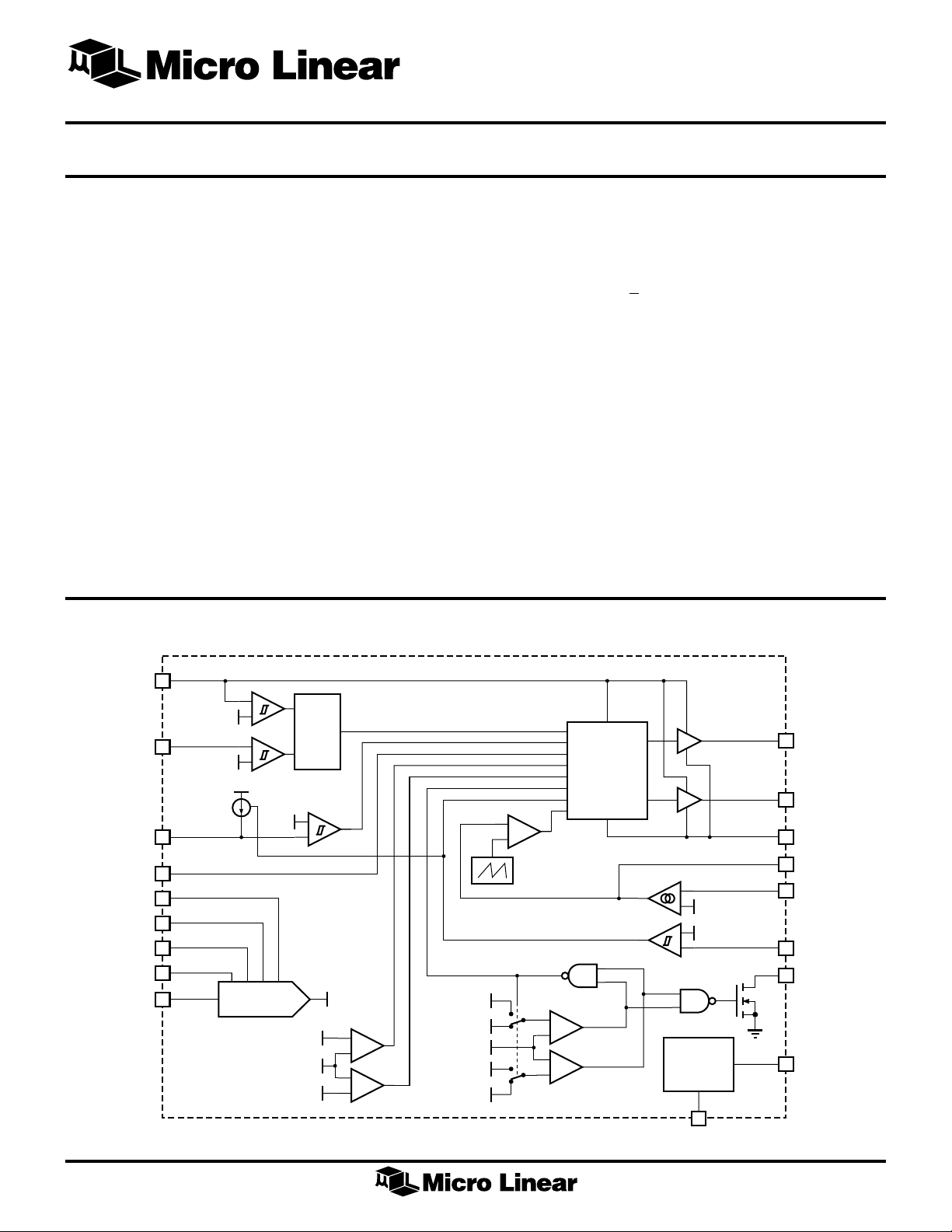
BLOCK DIAGRAM
FEATURES
■ Designed to meet Pentium Pro and Pentium II VRM
power supply requirements
■ DC regulation to +1% maximum
■ Proprietary circuitry provides transient response of ±5%
maximum over a 0A to 14A load range
■ Programmable output voltage (1.8V to 3.5V) is set by
an onboard 2 chord 4-bit D AC
■ Synchronous buck topology for maximum power
conversion efficiency
■ Fixed frequency operation for easier system integration
■ Integrated anti-shootthrough logic, short circuit
protection, shutdown, and UV lockout
V
DD
19
V
CC
18
PROTECT
20
SHDN
6
D0
1
D1
2
D2
3
D3
4
RANGE
5
10.5V
4.4V
30µA
+
–
+
–
5V
3.5V
2 CHORD
4 BIT DAC
V
DAC
V
DAC
UVLO
+ 3%
V
- 3%
P DRV
17
CONTROL
LOGIC
+
–
V
DAC
+
–
FB
+
–
V
V
DAC
V
DAC
DAC
V
DAC
+ 10%
+ 3%
- 10%
- 3%
+
–
200kHz
–
+
+
–
+
V
FB
–
+
–
3.5V
REFERENCE
10
PWR GND
V
DAC
-107mV
PWR GOOD
GND
N DRV
COMP
V
I
SENSE
V
REF
16
15
13
FB
11
12
8
9
1

ML4903
PIN CONFIGURATION
ML4903
20-Pin TSSOP (T20)
D0
D1
D2
D3
RANGE
SHDN
NC
PWR GOOD
V
REF
GND
1
2
3
4
5
6
7
8
9
10
PIN DESCRIPTION
PIN NAME FUNCTION
1 D0 LSB input to the DAC which sets the
output voltage
2 D1 Input to the DAC which sets the
output voltage
3 D2 Input to the DAC which sets the
output voltage
20
19
18
17
16
15
14
13
12
11
TOP VIEW
PIN NAME FUNCTION
9V
REF
PROTECT
V
DD
V
CC
P DRV
N DRV
PWR GND
NC
COMP
I
SENSE
V
FB
Bypass connection for the internal
3.5V reference
1 0 GND Analog signal ground
11 V
12 I
FB
SENSE
Output voltage feedback pin
Current sense input
4 D3 MSB input to the DAC which sets the
output voltage
5 RANGE Range selection bit for the 2 chord 4-
bit DAC. Logic 1 sets the range at
2.1V to 3.5V with an LSB of 100mV.
Logic 0 sets the range at 1.8V to
2.05V with an LSB of 50mV.
6 SHDN Grounding this pin shuts down the
regulator
8 PWR GOODThis open drain output goes low
whenever SHDN goes low or when
the output is not within +10% of its
nominal value
1 3 COMP Connection for the compensation and
optional soft-start delay network
15 PWR GND Power ground
1 6 N DRV Synchronous rectifier driver output
1 7 P DRV Buck switch driver output
18 V
CC
Connection point for monitoring the
5V supply to determine the proper
condition of PWR GOOD
19 V
DD
12V power supply input
20 PROTECT Connection for the integrating current
limit network
2
ABSOLUTE MAXIMUM RATINGS
ML4903
Absolute maximum ratings are those values beyond which
the device could be permanently damaged. Absolute
maximum ratings are stress ratings only and functional
device operation is not implied.
V
...........................................................................................
DD
V
..................................................................................................7V
CC
13.5V
Peak Dri ver Output Current.......................................±2A
Voltage...................................... GND - 0.3V to 5.5V
V
FB
I
Voltage.................................. GND - 0.5V to 5.5V
SENSE
All Other Inputs .................... GND - 0.3V to VDD + 0.3V
SHDN Input Current .............................................. 100mA
Junction T emperature.............................................. 150°C
Storage Temperature Range ..................... –65°C to 150°C
Lead Temperature (Soldering, 10 sec) .....................260°C
Thermal Resistance (
qJA).................................... 100°C/W
OPERATING CONDITIONS
T emper ature Range .......................................0°C to 70°C
VDD Range ..............................................11.4V to 12.6V
Range ...............................................4.75V to 5.25V
V
CC
ELECTRICAL CHARACTERISTICS
Unless otherwise specified, VDD = 12V, VCC = SHDN = 5V, TA = Operating Temperature Range (Note 1)
SYMBOL PARAMETER CONDITIONS MIN TYP MAX UNITS
REFERENCE
V
Output Voltage 3.51 3.535 3.56 V
REF
Line Regulation 11V < VDD < 13V 0.5 mV/V
UV LOCKOUT
VDD Start-up Threshold 10.0 10.5 10.8 V
VDD Hysteresis 30 0 450 6 00 mV
VCC Start-up Threshold 4.25 4.4 4.6 V
VCC Hysteresis 30 0 400 50 0 mV
SHUTDOWN
Input Low Voltage 0.8 V
Input High Voltage 2.0 V
Delay to Output 50 ns
POWER GOOD COMPARATOR
Output Voltage in Regulation 5kW pull-up to 5V 4.8 V
Output Voltage out of Regulation VFB < 90% V
Output Voltage in Shutdown SHDN = 0V, 5kW pull-up to 5V 0.4 V
BUCK REGULATOR
Oscillator Frequency 160 200 230 kHz
Duty Cycle Ratio RANGE = 1, V
or >110% V
DAC
= 0V, 80 98 %
DAC (D3-D0) Code = 0100
RANGE = 1, VFB > 3.193V, 0 %
DAC (D3-D0) Code = 0100
FB
DAC
0.4 V
DAC (RANGE, D3-D0) Input Low Voltage 0.8 V
DAC (RANGE, D3-D0) Input High Voltage 2.0 V
3
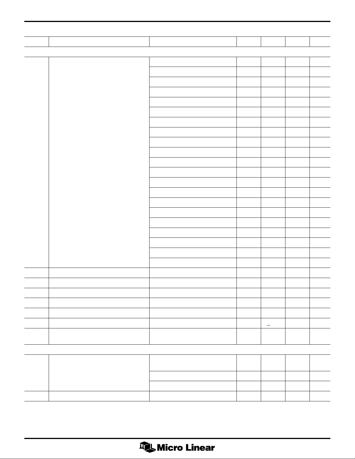
ML4903
ELECTRICAL CHARACTERISTICS (Continued)
SYMBOL PARAMETER CONDITIONS MIN TYP MAX UNITS
BUCK REGULATOR (Continued)
VFB Threshold Voltage (Note 2) RANGE = 0, (D3-D0) Code = 0000 2.050 2.071 2.092 V
RANGE = 0, (D3-D0) Code = 0001 2.000 2.020 2.04 V
RANGE = 0, (D3-D0) Code = 0010 1.950 1.970 1.989 V
RANGE = 0, (D3-D0) Code = 0011 1.900 1.919 1.938 V
RANGE = 0, (D3-D0) Code = 0100 1.850 1.869 1.887 V
RANGE = 0, (D3-D0) Code = 0101 1.800 1.818 1.836 V
RANGE = 1, (D3-D0) Code = 0000 3.500 3.535 3.570 V
RANGE = 1, (D3-D0) Code = 0001 3.400 3.434 3.468 V
RANGE = 1, (D3-D0) Code = 0010 3.300 3.333 3.366 V
RANGE = 1, (D3-D0) Code = 0011 3.200 3.232 3.264 V
RANGE = 1, (D3-D0) Code = 0100 3.100 3.131 3.162 V
RANGE = 1, (D3-D0) Code = 0101 3.000 3.030 3.060 V
RANGE = 1, (D3-D0) Code = 0110 2.900 2.929 2.958 V
SUPPLY
I
DD
RANGE = 1, (D3-D0) Code = 0111 2.800 2.828 2.856 V
RANGE = 1, (D3-D0) Code = 1000 2.700 2.727 2.754 V
RANGE = 1, (D3-D0) Code = 1001 2.600 2.626 2.652 V
RANGE = 1, (D3-D0) Code = 1010 2.500 2.525 2.550 V
RANGE = 1, (D3-D0) Code = 1011 2.400 2.424 2.448 V
RANGE = 1, (D3-D0) Code = 1100 2.300 2.323 2.346 V
RANGE = 1, (D3-D0) Code = 1101 2.200 2.222 2.244 V
RANGE = 1, (D3-D0) Code = 1110 2.100 2.121 2.142 V
I
Threshold Voltage -80 -117 mV
SENSE
I
Hysteresis 10 mV
SENSE
PROTECT Threshold Voltage 3.2 3.5 3.8 V
PROTECT Hysteresis 1.8 2 2.2 V
PROTECT Charging Current V(I
PROTECT Leakage Current +100 nA
Transition Time, C
P DRV and N DRV
VDD Current SHDN = 0V 650 900 µA
DAC (D3-D0) Code = 0000
) = -120mV 30 µA
SENSE
= 5000pF, 10-90% 40 ns
L
SHDN = 5V, VFB = 5V 1 2 mA
SHDN = 5V, VFB = 0V, CL = 5000pF 20 mA
I
Note 1: Limits are guaranteed by 100% testing, sampling, or correlation with worst case test conditions.
Note 2: Codes 00110 to 01111, and 11111 are not valid; applying these codes to the DAC will shut off P DRV and N DRV.
VCC Current 110µA
CC
4
 Loading...