

Micro Linear Corporation ML4895ES Datasheet
August 1996
FEATURING
Extended Commercial Temperature Range
-20˚C to 70˚C
for Portable Handheld Equipment
PRELIMINARY
ML4895
Synchronous Buck Controller
GENERAL DESCRIPTION
The ML4895 synchronous buck controller has been
designed to provide high efficiency DC/DC conversion for
portable products. The ML4895 can deliver a user
programmable 2.5V to 4V output from input voltages of
5.9V to 15V.
The ML4895 drives external P- and N-channel MOSFETs
in a synchronous buck topology, allowing an overall
conversion efficiency of greater than 90% over an output
current range exceeding three decades, with an output
current capability of up to 5A.
The regulator can be disabled via the SHDN pin. While
disabled, the output of the regulator is completely
isolated from the circuit’s input supply, and the supply
current is reduced to less than 5µA to help extend battery
life.
FEATURES
■ Regulation to ±3% maximum
■ Adjustable output synchronous buck (2.5V to 4V)
■ Wide input voltage range (5.9V to 15V)
■ Power conversion efficiencies of >90% over 3 decades
of output current
■ Integrated antishoot-through logic
■ Shutdown control provides load isolation and
minimum sleep mode power consumption
■ Low shutdown current
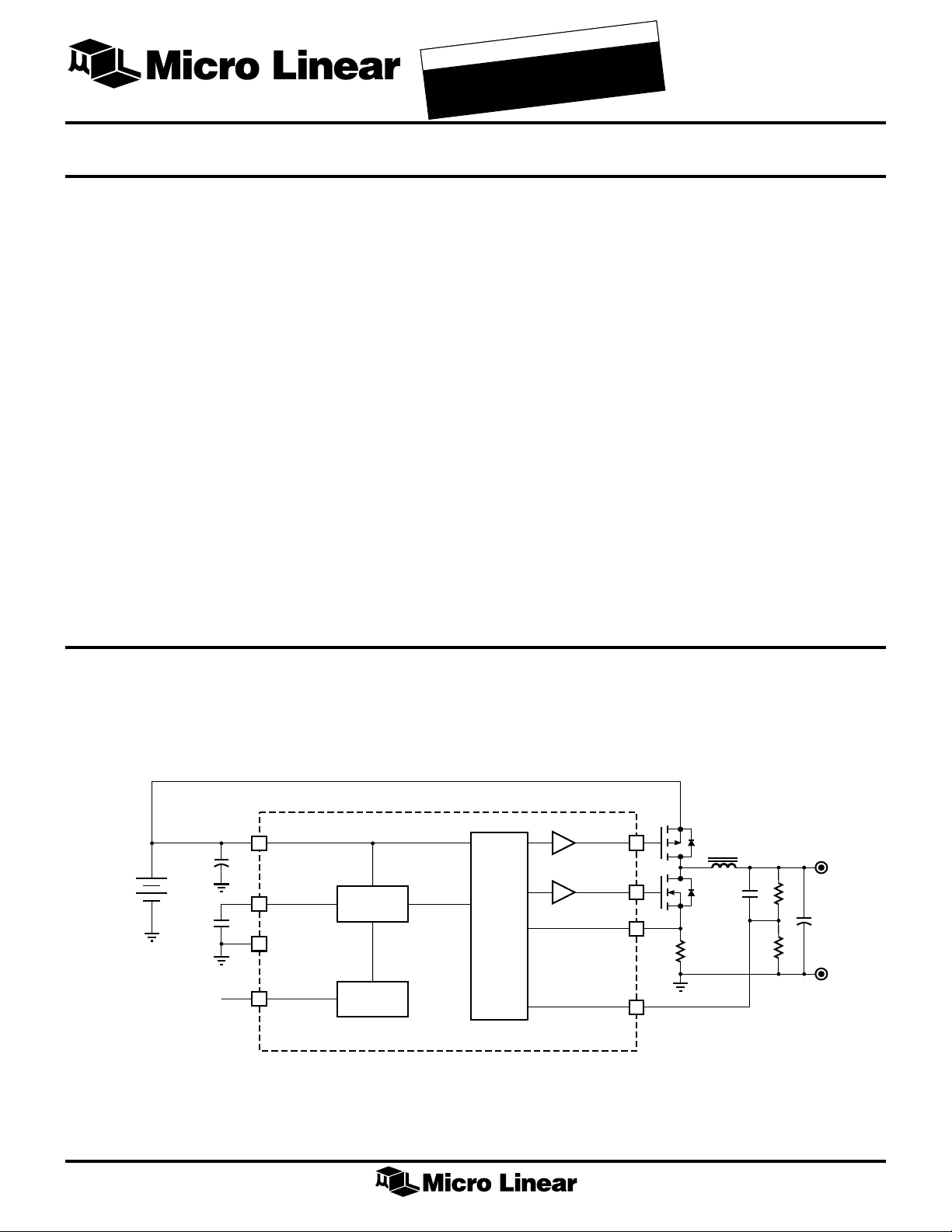
BLOCK DIAGRAM
V
IN
5.9V - 15V
FROM SYSTEM
POWER
MANAGEMENT
8
1
5
4
V
I
N
V
REG
GND
SHDN
BIAS
CIRCUITS
SLEEP
LOGIC
BUCK REGULATOR
P DRV
N DRV
I
SENSE
V
7
+
6
V
3
FB
2
OUT
2.5V - 4V
–
1
ML4895
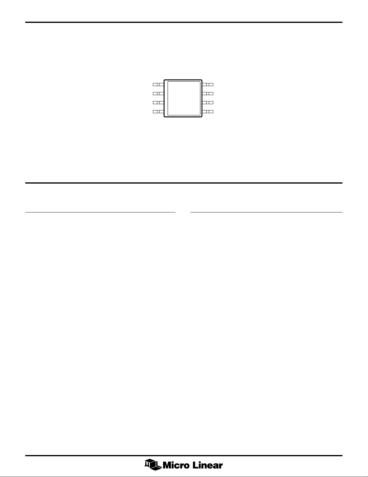
PIN CONFIGURATION
ML4895
8-Pin SOIC (S08)
PIN DESCRIPTION
PIN# NAME FUNCTION
1V
2V
3I
REG
FB
SENSE
Connection point for internal linear
regulator bypass capacitor
Programming pin for setting the
output voltage
Current sense input
V
REG
VFB
I
SENSE
SHDN
1
2
3
4
TOP VIEW
8
7
6
5
PIN# NAME FUNCTION
VIN
P DRV
N DRV
GND
5 GND Analog signal ground
6 N DRV NMOS driver output
7 P DRV PMOS driver output
8V
IN
Battery input voltage
4 SHDN a logic low on this pin shuts down the
regulator and all internal bias
circuitry for minimum power
consumption
2
ABSOLUTE MAXIMUM RATINGS
ML4895
Absolute maximum ratings are those values beyond
which the device could be permanently damaged.
Absolute maximum ratings are stress ratings only and
functional device operation is not implied.
V
............................................................................................ 16.5V
IN
Peak Driver Output Current....................................... ±2A
Junction Temperature............................................. 150°C
Storage Temperature Range .....................–65°C to 150°C
Lead Temperature (Soldering, 10 sec) .................... 150°C
Thermal Resistance (θ
) ....................................160°C/W
JA
OPERATING CONDITIONS
VFB Voltage .........................................GND - 0.3V to 6V
I
Voltage..................................................... +500mV
SENSE
All Other Inputs ..................... GND - 0.3V to VIN + 0.3V
SHDN Input Current .............................................100µA
VIN Range .................................................... 5.9V to 15V
V
Range ................................................... 2.5V to 4V
OUT
Temperature Range ................................... -20°C to 70°C
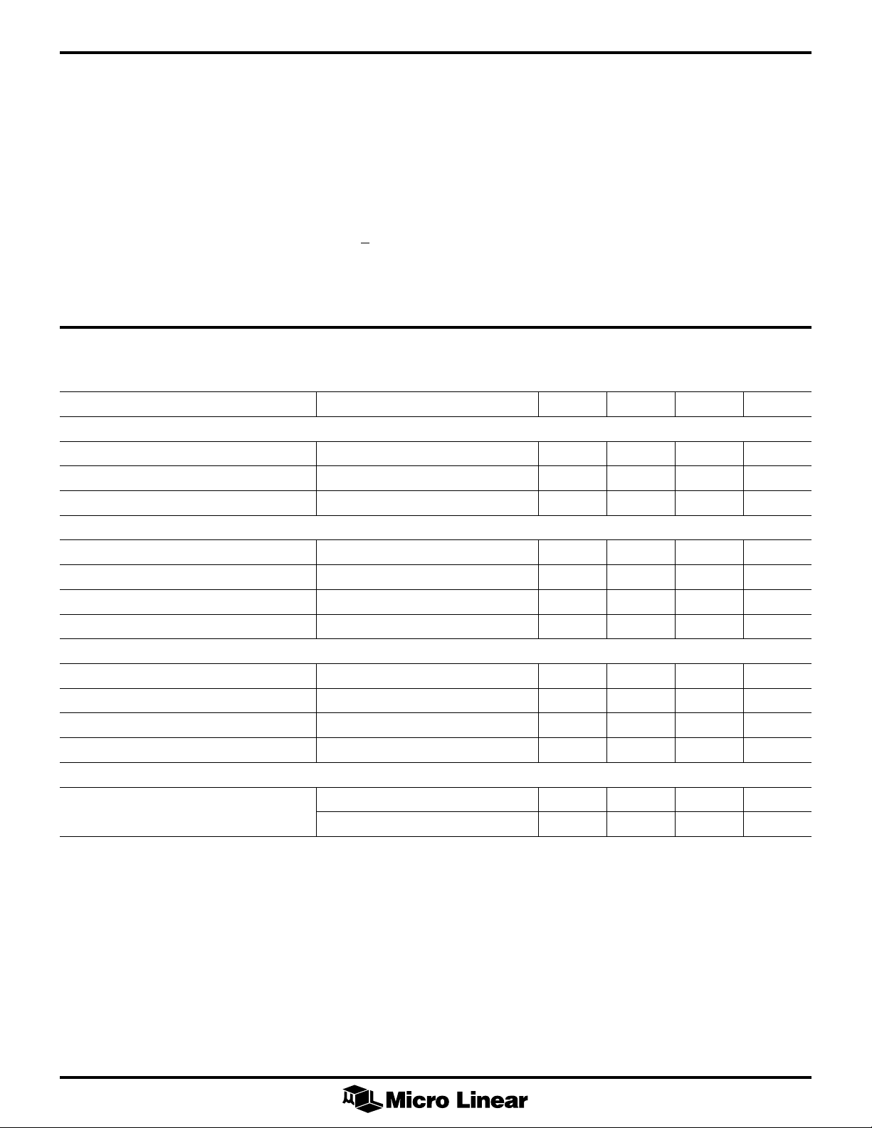
ELECTRICAL CHARACTERISTICS
Unless otherwise specified, VIN = 10V, TA = Operating Temperature Range (Note 1)
PARAMETER CONDITIONS MIN TYP MAX UNITS
LINEAR REGULATOR
Output Voltage TA = 25°C 3.29 3.33 3.37 V
Line Regulation 5.9V < VIN < 15V 1.7 4 mV/V
Total Variation Line, Temp 3.24 3.42 V
SHUTDOWN
Input Low Voltage 1.0 V
Input High Voltage 3.0 V
Input Low Current VIL = 0V 100 nA
Input High Current VIH = V
BUCK REGULATOR
Duty Cycle Ratio VIN = 5.9V, I
VFB Threshold Voltage 5.9V < VIN < 15V 2.425 2.5 2.575 V
I
Threshold Voltage -60 -80 -100 mV
SENSE
Transition Time CL = 1000 pF, GND to V
SUPPLY
VIN Current SHDN = 0V 2 5 µA
SHDN = 5V 300 750 µA
Note 1: Limits are guaranteed by 100% testing, sampling, or correlation with worst case test conditions.
IN
= VFB = 0V 75 97 %
SENSE
IN
50 100 ns
50 µA
3
 Loading...