

Datasheet ML4890ES-T, ML4890CS-5, ML4890CS-T, ML4890ES-3, ML4890ES-5 Datasheet (Micro Linear Corporation)
...
FEATURING
Extended Commercial Temperature Range
–20°C to 70°C
for Portable Handheld Equipment
April 1997
ML4890
High Efficiency, Low Ripple Boost Regulator
GENERAL DESCRIPTION
The ML4890 is a high efficiency, PFM (Pulse Frequency
Modulation), boost switching regulator connected in
series with an integrated LDO (Low Dropout Regulator)
that incorporates “Silent Switcher™” technology. This
technique incorporates a patented tracking scheme to
minimize the voltage drop across the LDO and increase
the total efficiency of the regulator beyond that which can
be obtained by using a discrete external LDO regulator.
The ML4890 is designed to convert single or multiple cell
battery inputs to regulated output voltages for integrated
circuits and is ideal for portable communications
equipment that cannot tolerate the output voltage ripple
normally associated with switching regulators.
An integrated synchronous rectifier eliminates the need for
an external Schottky diode and provides a lower forward
voltage drop, resulting in higher conversion efficiency.
FEATURES
■ Incorporates “Silent Switcher™” technology to deliver
very low output voltage ripple (typically 5mV)
■ Guaranteed full load start-up and operation at 1.0V
input and low operating quiescent current (<100µA)
for extended battery life
■ Pulse Frequency Modulation and internal synchronous
rectification for high efficiency
■ Minimum external components
■ Low ON resistance internal switching MOSFETs
■ 5V, 3.3V, and 3V output versions
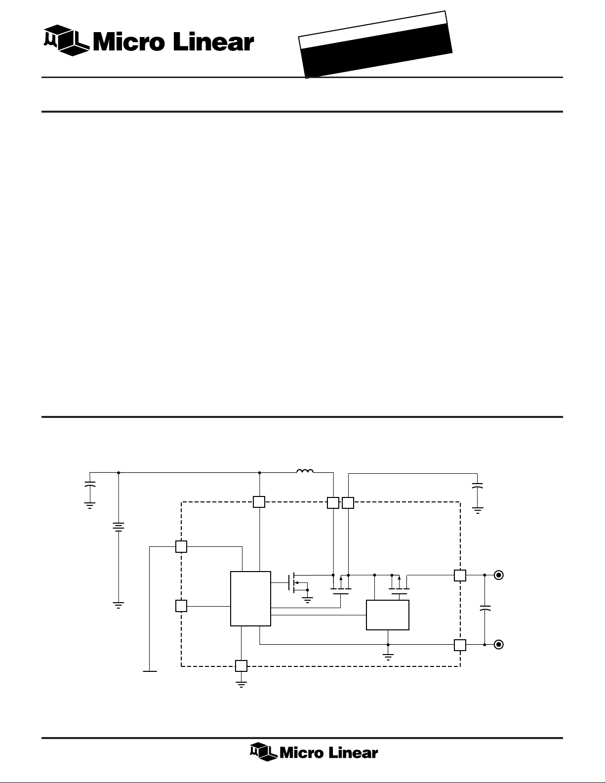
BLOCK DIAGRAM
*C
IN
V
BAT
FROM
POWER
MANAGEMENT
Patent Pending
7
2
SHDN
V
REF
V
IN
1
BOOST
CONTROL
GND
3
L1
5
6
V
L
FEEDBACK
V
BOOST
LDO
CONTROL
V
PWR
GND
OUT
C2
C1
+
V
OUT
–
4
8
*Optional
1
ML4890
PIN CONNECTION
ML4890-5/-3/-T
8-Pin SOIC (S08)
PIN DESCRIPTION
V
GND
V
OUT
V
IN
REF
1
2
3
4
TOP VIEW
8
7
6
5
PWR GND
SHDN
V
L
V
BOOST
PIN
NO. NAME FUNCTION
1V
IN
2V
REF
Battery input voltage
200mV reference output
3 GND Analog signal ground
4V
OUT
LDO linear regulator output
PIN
NO. NAME FUNCTION
5V
BOOST
Boost regulator output for connection
of an output filter capacitor
6V
L
Boost inductor connection
7 SHDN Pulling this pin high shuts down the
regulator, isolating the load from the
input
8 PWR GND Return for the NMOS boost transistor
2
ML4890
ABSOLUTE MAXIMUM RATINGS
Storage Temperature Range .................... –65°C to +150°C
Lead Temperature (Soldering 10s).......................... +260°C
Absolute maximum ratings are those values beyond which
the device could be permanently damaged. Absolute
maximum ratings are stress ratings only and functional
device operation is not implied.
V
Voltage on Any Other Pin ...GND –0.3V to V
Peak Switch Current (I
Average Switch Current (I
........................................................................ 7V
BOOST
) .......................................... 1A
PEAK
) ............................... 500mA
AVG
BOOST
+0.3V
LDO Output Current ............................................. 250mA
Junction Temperature .............................................. 150°C
Thermal Resistance (θ
Plastic SOIC .................................................... 110°C/W
OPERATING CONDITIONS
Temperature Range
ML4890CS-X ............................................ 0°C to +70°C
ML4890ES-X......................................... –20°C to +70°C
V
Operating Range
IN
ML4890CS-X ................................................ 1.0V to 6V
ML4890ES-X................................................. 1.1V to 6V
)
JA
ELECTRICAL CHARACTERISTICS
Unless otherwise specified, V
PARAMETER CONDITIONS MIN TYP. MAX UNITS
Supply
VIN Current VIN = 6V 60 75 µA
V
Quiescent Current V
OUT
VL Quiescent Current 1 µA
= Operating Voltage Range, TA = Operating Temperature Range. (Note 1)
IN
SHDN = high 15 25 µA
BOOST
= V
+ 0.5V 8 10 µA
OUT
Reference
Output Voltage (V
) 0 < I
REF
< –5µA, 195 200 205 mV
PIN2
PFM Regulator
Pulse Width (TON) 4.5 5 5.5 µs
LDO
DC Output Voltage (V
) ML4890-5 V
OUT
ML4890-3 V
ML4890-T V
BOOST
BOOST
BOOST
= V
= V
= V
OUT
OUT
OUT
+ 0.5V, I
+ 0.5V, I
+ 0.5V, I
< 200mA 4.85 5.0 5.15 V
OUT
< 100mA 3.2 3.3 3.4 V
OUT
< 80mA 2.91 3.0 3.09 V
OUT
Load Regulation ML4890-5 See Figure 1
= 1.2V, I
V
IN
VIN = 2.4V, I
ML4890-3 VIN = 1.2V, I
VIN = 2.4V, I
ML4890-T VIN = 1.2V, I
VIN = 2.4V, I
< 7mA 4.85 5.0 5.15 V
OUT
< 50mA 4.85 5.0 5.15 V
OUT
< 14mA 3.2 3.3 3.4 V
OUT
< 75mA 3.2 3.3 3.4 V
OUT
< 15mA 2.91 3.0 3.09 V
OUT
< 60mA 2.91 3.0 3.09 V
OUT
Dropout Voltage ML4890-5 See Figure 1
= 1.2V, I
V
IN
VIN = 2.4V, I
ML4890-3 VIN = 1.2V, I
VIN = 2.4V, I
ML4890-T VIN = 1.2V, I
VIN = 2.4V, I
Output Ripple 5mV
< 7mA 300 mV
OUT
< 50mA 500 mV
OUT
< 14mA 300 mV
OUT
< 75mA 500 mV
OUT
< 15mA 300 mV
OUT
< 60mA 500 mV
OUT
P-P
Shutdown
SHDN Threshold 0.5 0.8 1.0 V
SHDN Bias Current –100 100 nA
Note 1: Limits are guaranteed by 100% testing, sampling, or correlation with worst case conditions.
3
ML4890
V
IN
100µF
33µH
(Sumida CD54)
ML4890
V
PWR GND
IN
1µF
V
REF
GND
V
OUT
SHDN
V
BOOST
100µF
V
L
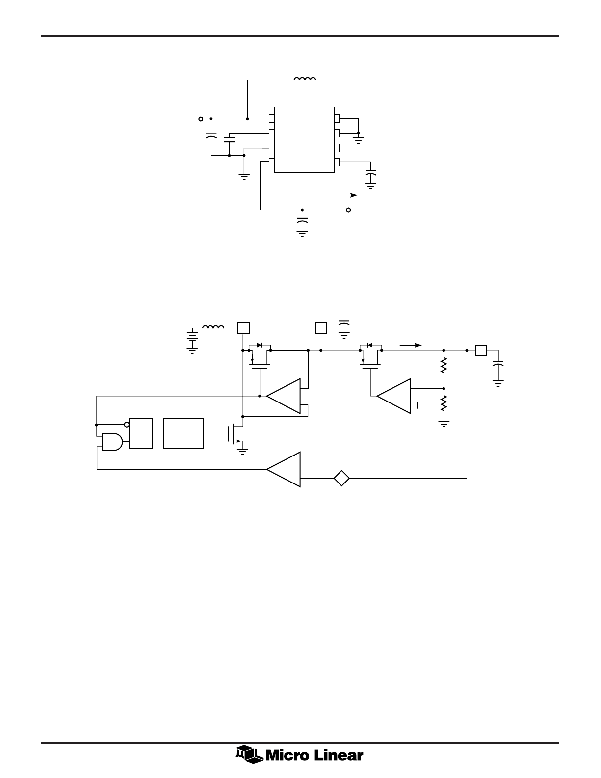
Figure 1. Application Test Circuit
33µF
I
OUT
V
OUT
OS
+
= f (I
C2
–
LOAD
I
LOAD
4
C1
REF
R1
R2
Q3
+
A3
–
V
)
L1
6
Q2
A2
R
S
5µs
ONE SHOT
Q1
A1
5
+
–
–
+
V
Figure 2. PFM Regulator and LDO Block Diagram
4

ML4890
Q(ONE SHOT)
Q1 ON Q1 ON
Q2
ON
Q2
ON
INDUCTOR
CURRENT
Q1 & Q2 OFF
FUNCTIONAL DESCRIPTION
The ML4890 combines Pulse Frequency Modulation
(PFM) and synchronous rectification to create a boost
converter that is followed by a low dropout linear
regulator (LDO). This combination creates a low output
ripple boost converter that is both highly efficient and
simple to use.
The PFM regulator charges a single inductor for a fixed
period of time and then completely discharges before
another cycle begins, simplifying the design by
eliminating the need for conventional current limiting
circuitry. Synchronous rectification is accomplished by
replacing an external Schottky diode with an on-chip
PMOS device, reducing switching losses and external
component count.
The integrated LDO reduces the output ripple voltage to
less than 5mV peak-to-peak. Integrating the LDO along
with the PFM regulator allows the circuit to be optimized
for very high efficiency using a patented feedback
technique. It also allows the LDO to provide the
maximum ripple rejection over the operating frequency
range of the regulator.
A block diagram of the ML4890 is shown in Figure 2. The
PFM stage is comprised of Q1, Q2, A1, A2, the one shot,
the flip-flop, and externals L1 and C2. The LDO stage is
comprised of Q3, A3, R1, R2, the offset voltage control,
and external C1. Since the LDO actually controls the
operation of the PFM regulator, the operation of the LDO
stage will be covered first.
Also included in the LDO stage is an offset voltage
control. This circuit monitors the output current and
adjusts the offset voltage according the general
characteristic shown in Figure 3. The offset control
ensures that the PFM stage provides just enough
“overhead” voltage for the LDO stage to operate properly.
PFM REGULATOR OPERATION
When the output of the PFM stage, V
above the dropout voltage, V
+ VOS, the output of A1
OUT
stays low and the circuit remains idle. When V
(pin 5), is at or
BOOST
BOOST
falls
below the required dropout voltage, the output of A1 goes
high, signaling the regulator to deliver charge to the
capacitor C2. Since the output of A2 is normally high, the
output of the flip-flop becomes SET. This triggers the one
shot to turn Q1 on and begins charging L1 for 5µs. When
the one shot times out, Q1 turns off, allowing L1 to
flyback and momentarily charge C2 through the body
diode of Q2. But, as the source voltage of Q2 rises above
the drain, the current sensing amplifier A2 drives the gate
of Q2 low, causing Q2 to short out the body diode. The
inductor then discharges into C2 through Q2. The output
of A2 going low also serves to RESET the flip-flop in
preparation for the next charging cycle. When the
inductor current in Q2 falls to zero, the output of A2 goes
high, releasing Q2‘s gate, allowing the flip-flop to be SET
again. If the voltage at V
is still low, A1 will initiate
BOOST
another pulse. Typical inductor current and voltage
waveforms are shown in Figure 4.
LDO OPERATION
The LDO stage operates as a linear regulator. A3 is the
error amplifier, which compares the output voltage
through the divider R1 and R2 to the reference, and Q3 is
the pass device. When the output voltage is lower than
desired, the output of A3 increases the gate drive of Q3,
which reduces the voltage drop across it and brings the
output back into regulation. Similarly, if the output voltage
is higher than desired, A3 adjusts the gate drive of Q3 for
more drop and the output is brought back into regulation.
450
400
350
(mV)
300
OS
V
250
200
150
100
0
10 20 30 40 50 60 70 80 90 100
Figure 4. PFM Inductor Current Waveforms and Timing.
SHUTDOWN
The SHDN pin should be held low for normal operation.
Raising the voltage on SHDN above the threshold level
will release the gate of Q3, which effectively becomes an
open circuit. This also prevents the one shot from
triggering, which keeps switching from occurring.
I
(mA)
OUT
Figure 3. LDO VOS versus output current.
5

ML4890
DESIGN CONSIDERATIONS
INDUCTOR
Selecting the proper inductor for a specific application
usually involves a trade-off between efficiency and
maximum output current. Choosing too high a value will
keep the regulator from delivering the required output
current under worst case conditions. Choosing too low a
value causes efficiency to suffer. It is necessary to know
the maximum required output current and the input
voltage range to select the proper inductor value. The
maximum inductor value can be estimated using the
following formula:
L
MAX
80
70
60
50
MAX (mA)
40
OUT
I
30
20
10
0
1.0
VT
=
()
2
×+×
2
××
() ()
IN MIN ON MIN
VVI
OUT OS OUT MAX
ML4890-T
L = 22µH
L = 15µH
L = 10µH
1.2 1.4 1.6 1.8 2.0 2.2 2.4 2.6 2.8
V
L = 33µH
(V)
IN
η
()
L = 47µH
L = 68µH
(1)
where η is the efficiency, typically between 0.75 and
0.85, and VOS is the dropout voltage at I
OUT(MAX)
taken
from Figure 3. Note that this is the value of inductance
that just barely delivers the required output current under
worst case conditions. A lower value may be required to
cover inductor tolerance, the effect of lower peak inductor
currents caused by resistive losses, and minimum dead
time between pulses.
Another method of determining the appropriate inductor
value is to make an estimate based on the typical
performance curves given in Figures 5 and 6. Figure 5
shows maximum output current as a function of input
voltage for several inductor values. These are typical
performance curves and leave no margin for inductance
and ON-time variations. To accommodate worst case
conditions, it is necessary to derate these curves by at
least 10% in addition to inductor tolerance.
ML4890-3
100
90
80
70
60
50
MAX (mA)
40
OUT
I
30
20
10
0
1.0
L = 10µH
L = 15µH
1.5 2.0 2.5 3.0
VIN (V)
L = 22µH
L = 33µH
L = 47µH
L = 68µH
ML4890-5
200
180
160
140
120
100
MAX (mA)
80
OUT
I
60
40
20
0
1.0
L = 15µH
L = 10µH
1.5 2.0 2.5 3.0 3.5 4.0 4.5
(V)
V
IN
L = 22µH
L = 33µH
L = 47µH
L = 68µH
Figure 5. Output Current versus Input Voltage.
6

ML4890
For example, a two cell to 5V application requires 40mA
of output current while using an inductor with 15%
tolerance. The output current should be derated by 25%
to 50mA to cover the combined inductor and ON-time
tolerances. Assuming that 2V is the end of life voltage of a
two cell input, Figure 5 shows that with a 2V input, the
ML4890-5 delivers 58mA with a 22µH inductor.
Figure 6 shows efficiency under the conditions used to
create Figure 5. It can be seen that efficiency is mostly
independent of input voltage and is closely related to
inductor value. This illustrates the need to keep the
inductor value as high as possible to attain peak system
efficiency. As the inductor value goes down to 10µH, the
efficiency drops to between 70% and 75%. With 33µH,
the efficiency reaches approximately 85% and there is
little room for improvement. At values greater than 47µH,
the operation of the synchronous rectifier becomes
unreliable at low input voltages because the inductor
current is so small that it is difficult for the control circuitry
to detect. The data used to generate Figures 5 and 6 is
provided in Table 1.
ML4890-T
95
After the appropriate inductor value is chosen, it is
necessary to find the minimum inductor current rating
required. Peak inductor current is determined from the
following formula:
I
L PEAK
()
TV
ON MAX IN MAX
=
×
() ()
L
MIN
(2)
It is important to note that for reliable operation, make
sure that I
does not exceed the 1A maximum switch
L(PEAK)
current rating. In the two cell application previously
described, a maximum input voltage of 3V would give a
peak current of 880mA. When comparing various
inductors, it is important to keep in mind that suppliers
use different criteria to determine their ratings. Many use a
conservative current level, where inductance has dropped
to 90% of its normal level. In any case, it is a good idea to
try inductors of various current ratings with the ML4890 to
determine which inductor is the best choice. Check
efficiency and maximum output current, and if a current
probe is available, look at the inductor current to see if it
looks like the waveform shown in Figure 4.
ML4890-3
95
L = 68µH
90
MAX (%)
85
80
75
70
65
1.0
L = 33µH
L = 22µH
L = 15µH
L = 10µH
OUT
Efficiency at I
L = 47µH
1.2 1.4 1.6 1.8 2.0 2.2 2.4 2.6 2.8
VIN (V)
95
90
85
MAX (%)
OUT
80
75
Efficiency at I
L = 10µH
70
ML4890-5
L = 15µH
L = 68µH
L = 47µH
L = 22µH
90
L = 47µH
MAX (%)
85
L = 33µH
OUT
L = 22µH
80
L = 15µH
75
Efficiency at I
L = 10µH
70
65
1.0
L = 33µH
L = 68µH
1.5 2.0 2.5 3.0
(V)
V
IN
65
60
1.0
1.5 2.0 2.5 3.0 3.5 4.0 4.5
Figure 6. Typical Efficiency as a Function of VIN.
7

ML4890
The DC resistance of the inductor should be kept to a
minimum to reduce losses. A good rule of thumb is to
allow 5 to 10mΩ of resistance for each µH of inductance.
Also, be aware that the DC resistance of an inductor
usually isn‘t specified tightly, so an inductor with a
maximum DC resistance spec of 150mΩ may actually
have 100mΩ of resistance.
Suitable inductors can be purchased from the following
suppliers:
Coilcraft (708) 639-6400
Coiltronics (407) 241-7876
Dale (605) 665-9301
Sumida (708) 956-0666
BOOST CAPACITOR
The boost capacitor (C2) supplies current to the load
during the ON-time of Q1 and will limit the ripple the
LDO stage has to contend with. The ripple on C2 is
influenced by three capacitor parameters: capacitance,
ESL, and ESR. The contribution due to capacitance can be
determined by looking at the change in the capacitor
voltage required to store the energy delivered by the
inductor in a single charge-discharge cycle, as given by
the following formula:
22
TV
×
C
2
≥
LV V V
2
×× ×∆ (–)
ON IN
BOOST OUT IN
inFarads
()
(3)
For example, a 2.4V input, a 5V output, a 22µH inductor,
and an allowance of 100mV of ripple on the boost
capacitor results in a minimum C2 value of 15µF.
The boost capacitor‘s Equivalent Series Resistance (ESR)
and Equivalent Series Inductance (ESL), also contribute to
the ripple due to the inductor discharge current waveform.
Just after the NMOS transistor turns off, the output current
ramps quickly to match the peak inductor current. This
fast change in current through the boost capacitor‘s ESL
causes a high frequency (5ns) spike that can be over 1V in
magnitude. After the ESL spike settles, the boost voltage
still has a ripple component equal to the inductor
discharge current times the ESR. This component will have
a sawtooth waveshape and can be calculated using the
following formula:
For example, a 2.4V input, a 22µH inductor, and an
allowance of 100mV of ripple on the boost capacitor
results in a maximum ESR of 200mΩ. Therefore, a boost
capacitor with a capacitance of 22µF or 33µF, an ESR of
less than 200mΩ, and an ESL of less than 5nH is a good
choice. Tantalum capacitors which meet these
requirements can be obtained from the following
suppliers:
AVX (207) 282-5111
Sprague (207) 324-4140
OUTPUT CAPACITOR
The LDO stage output capacitor (C1) is required for
stability and to provide a high frequency filter. An output
capacitor with a capacitance of 100µF, an ESR of less than
100mΩ, and an ESL of less than 5nH is a good general
purpose choice.
INPUT CAPACITOR
Unless the input source is a very low impedance battery, it
will be necessary to decouple the input with a capacitor
with a value of between 47µF and 100µF. This provides
the benefits of preventing input ripple from affecting the
ML4890 control circuitry, and it also improves efficiency
by reducing I-squared R losses during the charge and
discharge cycles of the inductor. Again, a low ESR
capacitor (such as tantalum) is recommended.
REFERENCE CAPACITOR
Under some circumstances input ripple cannot be
reduced effectively. This occurs primarily in applications
where inductor currents are high, causing excess output
ripple due to “pulse grouping”, where the chargedischarge pulses are not evenly spaced in time. In such
cases it may be necessary to decouple the reference pin
(V
) with a small 10nF to 100nF ceramic capacitor. This
REF
is particularly true if the ripple voltage at VIN is greater
than 100mV.
V
∆
ESR
BOOST
≤Ω
I
L PEAK
()
in
()
(4)
8

LAYOUT
Good PC board layout practices will ensure the proper
operation of the ML4890. Important layout considerations
include:
• Use adequate ground and power traces or planes
• Keep components as close as possible to the ML4890
• Use short trace lengths from the inductor to the VL pin
and from the output capacitor to the V
• Use a single point ground for the ML4890 ground pins,
and the input and output capacitors
A sample PC board layout is shown in Figure 7.
BOOST
pin.
ML4890
Figure 7. Sample PC Board Layout.
9

ML4890
TABLE 1. MAXIMUM OUTPUT CURRENT AND EFFICIENCY
ML4890-T ML4890-3
V
IN
L = 10µH
1.0 30.6 73.5
1.5 70.7 72.0
2.0 80.0 70.3
L = 15µH
1.0 23.8 78.7
1.5 56.5 77.3
2.0 80.0 74.9
2.5 80.0 74.0
2.8 80.0 73.7
L = 22µH
1.0 18.4 82.0
1.5 44.2 81.1
2.0 76.6 77.9
2.5 80.0 76.9
2.8 80.0 76.7
L = 33µH
1.0 13.0 85.7
1.5 32.4 85.1
2.0 56.6 82.7
2.5 80.0 80.4
2.8 80.0 80.1
L = 47µH
1.0 9.8 87.4
1.5 23.3 87.2
2.0 41.1 85.8
2.5 62.9 83.7
2.8 77.4 82.6
L = 68µH
1.0 7.9 88.4
1.5 18.8 88.9
2.0 33.4 87.6
2.5 51.0 86.0
2.8 64.3 84.6
I
(mA) EFFICIENCY PERCENTAGE
OUT
V
IN
L = 10µH
1.0 29.6 73.8
1.5 71.4 73.7
2.0 100.0 71.9
L = 15µH
1.0 23.0 80.4
1.5 54.7 78.8
2.0 89.8 76.1
2.5 100.0 74.7
3.0 100.0 74.1
L = 22µH
1.0 16.2 82.1
1.5 41.4 82.6
2.0 75.6 80.5
2.5 100.0 77.7
3.0 100.0 77.1
L = 33µH
1.0 10.9 85.0
1.5 30.4 86.0
2.0 55.8 84.7
2.5 82.5 82.3
3.0 100.0 80.3
L = 47µH
1.0 9.1 87.1
1.5 22.7 87.9
2.0 41.9 87.4
2.5 63.3 85.6
3.0 89.6 83.1
L = 68µH
1.0 7.7 89.3
1.5 17.9 89.2
2.0 32.1 88.3
2.5 48.8 87.2
3.0 69.6 85.9
I
(mA) EFFICIENCY PERCENTAGE
OUT
10

TABLE 1. MAXIMUM OUTPUT CURRENT AND EFFICIENCY (continued)
ML4890-5
ML4890
V
IN
L = 10µH
1.0 13.6 67.9
1.5 42.7 77.2
2.0 82.2 78.1
L = 15µH
1.0 9.3 69.6
1.5 31.7 80.9
2.0 60.6 81.6
2.5 95.7 80.5
3.0 137.9 79.4
L = 22µH
1.0 7.4 73.6
1.5 23.1 83.6
2.0 46.1 84.6
2.5 73.9 84.0
3.0 108.9 83.0
3.5 145.1 82.4
4.0 184.5 81.3
4.5 200.0 80.1
L = 33µH
1.0 6.0 76.9
1.5 18.3 85.8
2.0 34.2 86.8
2.5 57.0 86.6
3.0 82.3 86.2
3.5 106.0 85.3
4.0 137.1 84.6
4.5 169.3 84.0
L = 47µH
1.0
1.5 14.2 87.2
2.0 25.7 88.3
2.5 41.4 88.3
3.0 59.4 88.0
3.5 82.9 87.3
4.0 105.5 86.6
4.5 131.3 86.2
L = 68µH
1.0
1.5
2.0 17.9 88.9
2.5 31.7 89.8
3.0 46.2 89.7
3.5 63.2 89.6
4.0 82.5 89.2
4.5 99.7 88.0
I
(mA) EFFICIENCY PERCENTAGE
OUT
11

ML4890
PHYSICAL DIMENSIONS inches (millimeters)
0.189 - 0.199
(4.80 - 5.06)
8
Package: S08
8-Pin SOIC
0.017 - 0.027
(0.43 - 0.69)
(4 PLACES)
0.055 - 0.061
(1.40 - 1.55)
PIN 1 ID
1
0.050 BSC
(1.27 BSC)
0.012 - 0.020
(0.30 - 0.51)
SEATING PLANE
0.148 - 0.158
(3.76 - 4.01)
0.059 - 0.069
(1.49 - 1.75)
0.228 - 0.244
(5.79 - 6.20)
0.004 - 0.010
(0.10 - 0.26)
0º - 8º
0.015 - 0.035
(0.38 - 0.89)
0.006 - 0.010
(0.15 - 0.26)
ORDERING INFORMATION
PART NUMBER OUTPUT VOLTAGE TEMPERATURE RANGE PACKAGE
ML4890CS-T 3.0V 0°C to +70°C 8-Pin SOIC (S08)
ML4890CS-3 3.3V 0°C to +70°C 8-Pin SOIC (S08)
ML4890CS-5 5.0V 0°C to +70°C 8-Pin SOIC (S08)
ML4890ES-T 3.0V –20°C to +70°C 8-Pin SOIC (S08)
ML4890ES-3 3.3V –20°C to +70°C 8-Pin SOIC (S08)
ML4890ES-5 5.0V –20°C to +70°C 8-Pin SOIC (S08)
© Micro Linear 1997 is a registered trademark of Micro Linear Corporation
Products described in this document may be covered by one or more of the following patents, U.S.: 4,897,611; 4,964,026; 5,027,116; 5,281,862; 5,283,483; 5,418,502; 5,508,570; 5,510,727; 5,523,940;
5,546,017; 5,559,470; 5,565,761; 5,592,128; 5,594,376; Japan: 2598946; 2619299. Other patents are pending.
Micro Linear reserves the right to make changes to any product herein to improve reliability, function or design.
Micro Linear does not assume any liability arising out of the application or use of any product described herein,
neither does it convey any license under its patent right nor the rights of others. The circuits contained in this
data sheet are offered as possible applications only. Micro Linear makes no warranties or representations as to
whether the illustrated circuits infringe any intellectual property rights of others, and will accept no responsibility
or liability for use of any application herein. The customer is urged to consult with appropriate legal counsel
before deciding on a particular application.
12
2092 Concourse Drive
San Jose, CA 95131
Tel: 408/433-5200
Fax: 408/432-0295
DS4890-01
 Loading...