

Micro Linear Corporation ML4880CS, ML4880ES Datasheet
FEATURING
Extended Commercial Temperature Range
–20°C to 70°C
for Portable Handheld Equipment
July 2000
ML4880*
Portable PC/PCMCIA Power Controller
GENERAL DESCRIPTION
The ML4880 Portable PC and PCMCIA Power Controller
is a complete solution for DC/DC power conversion for
portable computing systems with single or multiple
PCMCIA slots.
The device provides two synchronous buck controllers to
implement mixed voltage systems and a flyback controller
for 12V VPP generation for PCMCIA slots. The flyback
architecture enables generation of high currents (150mA
or more per slot) on the 12V bus for multiple slot PCMCIA
applications.
Each regulator can be independently switched off to fully
isolate the load from the power supply. The PFM
FEATURES
■Regulation to ±3% maximum: provides 2% PCMCIA
switch matrix margin
■ Two synchronous buck controllers for 3.3/3V, 5V
generation, and a flyback for high current, 12V
generation from 5.5V to 18V input
■ Regulator power conversion efficiencies > 90%
■ Pulse frequency modulation for high efficiency
operation
■ Independent regulator shutdown for full load isolation
■ Adjustable current limit
■ Wide input voltage range (5.5V to 18V)
architecture will automatically adjust switching frequency
at light loads in order to maintain power conversion
efficiencies in excess of 90% over a wide output power
range. (* Indicates Part is End Of Life as of July 1, 2000)
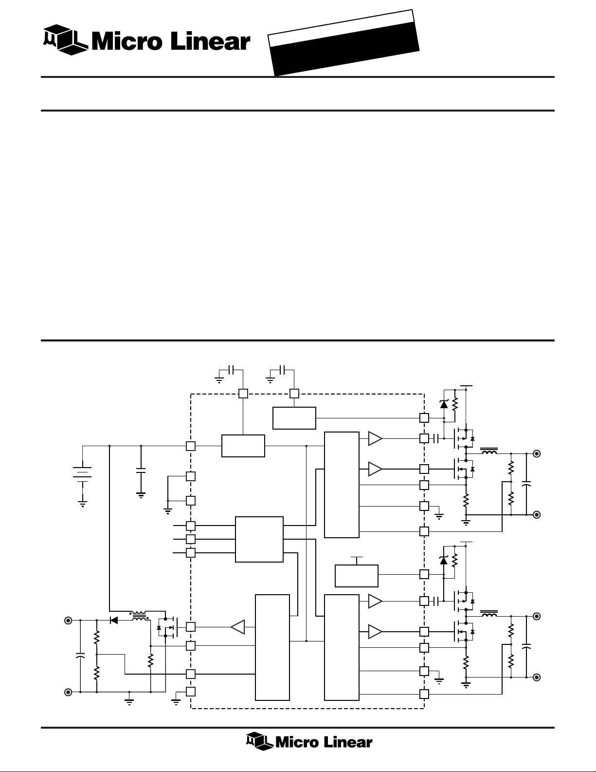
BLOCK DIAGRAM
V
IN
V
IN
5.5 – 18V
+
V
C
OUT
6V – 15V
–
TO SYSTEM
POWER
MANAGEMENT
V
IN
16
6
GND
7
GND
SHDN A
11
SHDN B
18
SHDN C
10
N DRV C
17
I
SENSE
3
V
FB
12
21
PWR GND C
C
C
15
V
BIAS
CIRCUITS
SHUTDOWN
LOGIC
REG
GATE
CLAMP
FLYBACK REGULATOR C
24
CLAMP
BUCK REGULATOR ABUCK REGULATOR B
CLAMP
GATE
CLAMP
CLAMP A
P DRV A
N DRV A
I
SENSE
PWR GND A
VFB A
CLAMP B
P DRV B
N DRV B
I
SENSE
PWR GND B
VFB B
2
13
14
A
4
23
9
1
19
20
B
5
22
8
V
IN
+
V
A
OUT
2.5 – 3.5V
–
+
V
B
OUT
4.5 – 5.0V
–
1
ML4880
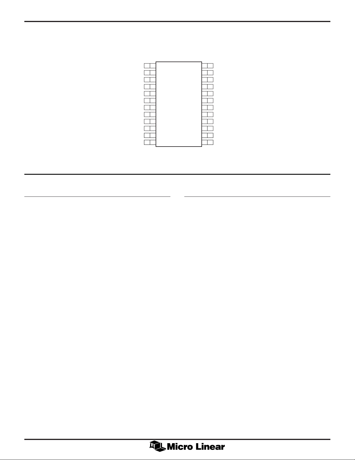
PIN CONFIGURATION
ML4880
24-Pin SOIC (S24)
CLAMP B
CLAMP A
I
SENSE
I
SENSE
I
SENSE
GND
GND
V
FB
V
FB
SHDN C
SHDN A
V
FB
1
2
C
A
B
B
A
C
3
4
5
6
7
8
9
10
11
12
TOP VIEW
24
23
22
21
20
19
18
17
16
15
14
13
CLAMP
PWR GND A
PWR GND B
PWR GND C
NDRV B
PDRV B
SHDN B
NDRV C
V
IN
V
REG
NDRV A
PDRV A
PIN DESCRIPTION
PIN# NAME FUNCTION PIN# NAME FUNCTION
1 CLAMP B Gate clamp, regulator B
2 CLAMP A Gate clamp, regulator A
3I
4I
5I
C Current sense, regulator C
SENSE
A Current sense, regulator A
SENSE
B Current sense, regulator B
SENSE
6 GND Ground
7 GND Ground
8VFB B Feedback node, buck regulator B
9VFB A Feedback node, buck regulator A
10 SHDN C Shutdown input, regulator C
11 SHDN A Shutdown input, regulator A
12 VFB C Feedback node, regulator C
13 PDRV A P-channel drive, regulator A
14 NDRV A N-channel drive, regulator A
15 V
16 V
REG
IN
Linear regulator output
Power supply input voltage
17 NDRV C N-channel drive, regulator C
18 SHDN B Shutdown input, regulator B
19 PDRV B P-channel drive, regulator B
20 NDRV B N-channel drive, regulator B
21 PWR GND C Power Ground, regulator C
22 PWR GND B Power Ground, regulator B
23 PWR GND A Power Ground, regulator A
24 CLAMP Charge pump capacitor input
2

ML4880
ABSOLUTE MAXIMUM RATINGS
Absolute maximum ratings are those values beyond
which the device could be permanently damaged.
Absolute maximum ratings are stress ratings only and
functional device operation is not implied.
V
............................................................................................... 20V
IN
OPERATING CONDITIONS
VIN Range ..................................................... 5.5V to 18V
Temperature Range
ML4880CS ................................................ 0°C to 70°C
ML4880ES ............................................. –20°C to 70°C
Peak Driver Output Current ........................................ 2A
VFB Voltage .........................................GND – 0.3V to 6V
I
Voltage..................................................... ±500mV
SENSE
All Other Analog Inputs ......... GND – 0.3V to VIN + 0.3V
All Digital Inputs .................. GND – 0.3V to V
REG
+ 0.3V
Junction Temperature ............................................. 150°C
Storage Temperature Range .................... –65°C to 150°C
Lead Temperature (Soldering, 10 sec) ..................... 150°C
Thermal Resistance (θJA)...................................... 80°C/W
ELECTRICAL CHARACTERISTICS
Unless otherwise specified, V
PARAMETER CONDITIONS MIN TYP MAX UNITS
Shutdown Inputs
Input Low Voltage 0.8 V
Input High Voltage 2.0 V
Input Bias Current –1 1 µA
Buck Regulator A
Duty Cycle Ratio VIN = 5.5V, I
VFB A Threshold Voltage 1.21 1.25 1.29 V
I
A Threshold Voltage –140 –200 –250 mV
SENSE
Transition Time CL = 1000pF, 0 to V
Buck Regulator B
Duty Cycle Ratio VIN = 5.5V, I
VFB B Threshold Voltage 1.21 1.25 1.29 V
I
B Threshold Voltage –140 –200 –250 mV
SENSE
Transition Time CL = 1000pF, 0 to V
Flyback Regulator C
Duty Cycle Ratio VIN = 5.5V, I
VFB C Threshold Voltage 1.21 1.25 1.29 V
I
C Threshold Voltage –140 –200 –250 mV
SENSE
Transition Time CL = 1000pF, 0 to V
Supply
Linear Regulator Output Voltage 7V ≤ VIN ≤ 18V 6.25 6.99 V
Linear Regulator Load Regulation I(V
VIN Current SHDN A/B/C = 5V 300 350 µA
= 14V, C(V
IN
) = 10µF, T
REG
VIN = 18V, I
) = 0 to 10mA 6.10 6.99 V
REG
SHDN A/B/C = 0V 350 400 µA
= Operating Temperature Range (Note 1)
A
A = VFB A = 0V 86 96 %
SENSE
REG
B = VFB B = 0V 92 98 %
SENSE
REG
C = VFBC = 0V 86 94 %
SENSE
C = VFBC = 0V 61 77 %
SENSE
REG
80 100 ns
80 100 ns
80 100 ns
Note 1: Limits are guaranteed by 100% testing, sampling or correlation with worst case test conditions.
3
ML4880
FUNCTIONAL DESCRIPTION
The ML4880 converts a 5.5V to 18V input to three outputs
via two synchronous buck controllers and a flyback
controller. The two buck controllers utilize a unique
current mode PFM control architecture that generate
output voltages in the range of 2.5V to 3.5V (output A),
and 4.5V to 5V (output B). The output current is set by
external components, and can exceed 2A on each supply.
The flyback controller also uses a current mode PFM
control scheme and can be used to generate a 6V to 15V
output. Again, the output current of the flyback is
dependent on external components, and output currents
of 500mA are obtainable. Even at light loads, the PFM
architecture maintains high conversion efficiencies over a
wide range of input voltages. If it is necessary to further
extend battery life, the user can shutdown and fully
disconnect each load from the input independently.
BIAS CIRCUITS
The bias circuits are comprised of a linear regulator and a
precision voltage reference. The linear regulator produces
a supply voltage (V
V
pin should be bypassed to GND with a 4.7µF to
REG
10µF capacitor. The precision voltage reference is used by
the feedback circuit of each controller to maintain an
accurate output voltage.
) used by the control circuits. The
REG
GATE CLAMP
The gate clamp circuit provides a method of preventing
the buck regulator P-channel MOSFET switches from
accidentally turning on when the input is suddenly
switched to a higher voltage. This condition can occur
during start-up or when an adapter voltage is applied. As
shown in the block diagram, the P DRV drivers are
capacitively coupled to the gates.
Assume that P DRV is in the OFF state, or at V
REG
, and the
gate voltage is held at VIN through the resistor. The gatesource voltage of the MOSFET is 0V and the switch stays
off. If a higher input voltage (VIN + 5V for example) is
suddenly applied with P DRV still in the OFF state, the
source voltage of the MOSFET would jump up to VIN +
5V, but the gate would still be at VIN. The gate-source
voltage becomes –5V and the P-channel MOSFET would
turn on even though P DRV is still in the OFF state. In
order to prevent the MOSFET from turning on, the gate
clamp circuit senses the increase in the input voltage and
pumps charge into the gate side of the coupling capacitor,
quickly charging the capacitor to the new input voltage
level.
The CLAMP pin requires a capacitor to GND in order for
the gate clamp circuit to function properly. The capacitor
value should be 1.5 to 2 times the value used for the
coupling capacitor.
SHUTDOWN LOGIC
Each controller has a separate shutdown pin. By applying
a logic high to the appropriate pin, the transconductance
amplifier and current comparator of each controller
(shown in Figures 1 and 3) can be disabled. This prevents
switching from occurring and disconnects the load from
the input. All other circuitry within the ML4880 remains
active during shutdown.
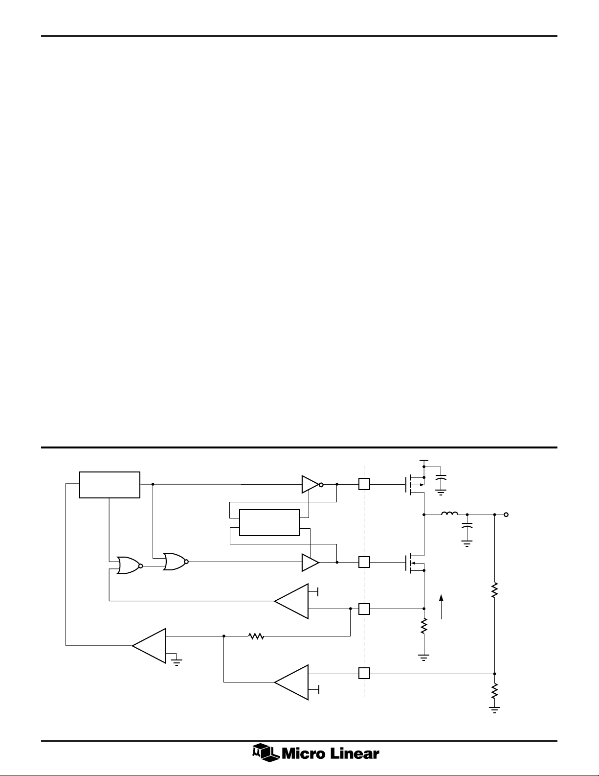
T
OSCILLATOR/
ONE SHOT
V
CURRENT
COMPARATOR
ON
SHOOT THRU
PROTECTION
SYNCHRONOUS
RECTIFIER
COMPARATOR
V
SR
Rgm
C
+
–
TRANSCONDUCTANCE
AMPLIFIER
BUCK CONTROLLERS
A block diagram of the buck controllers is shown in Figure
1. The circuit utilizes a constant ON-time PFM control
architecture. The circuit determines the OFF-time by
waiting for the inductor current to drop to a level set by
the feedback voltage (VFB).
V
IN
C
R
SENSE
IN
L
V
OUT
C
OUT
R1
I
L
P DRV
N DRV
–18mV
+
I
–
–
SENSE
V
FB
+
1.25V
R2
Figure 1. Buck Controller Functional Diagram
4
ML4880
The oscillator/one shot block generates a constant ONtime and a minimum OFF-time. The OFF-time is extended
for as long as the output of the current comparator stays
low. Note that the inductor current flows in the current
sense resistor during the OFF-time. Therefore, a minimum
OFF-time is required to allow for the finite circuit delays
in sensing the inductor current. The ON-time is triggered
when the current comparator’s output goes high.
However, unlike conventional fixed ON-time controllers,
the ML4880’s one shot has an inverse relationship with
the input voltage as shown in Figure 4. Figure 5 plots the
inductor voltage-ON-time product. Note that the voltsecond product is nearly constant at voltages above 7V
input. This results in an inductor current ripple of:
TVV
×−()
ON IN OUT
∆I
=
L
L
(1)
It is important to note that the ripple current does not vary
in proportion with VIN, but remains nearly constant over a
wide input voltage range.
The transconductance amplifier generates a current from
the voltage difference between the reference and the
feedback voltage, VFB. This current produces a voltage
across Rgm that adds to the negative voltage that is
developed across the current sense resistor. When the
current level in the inductor drops low enough (a less
negative sense voltage) to cause the voltage at the noninverting input of the current comparator to go positive,
the comparator trips and starts a new ON cycle. In other
words, the current programming comparator controls the
length of the OFF-time by waiting until the inductor
current decreases to a value determined by the
transconductance amplifier.
This technique allows the feedback transconductance
amplifier’s output current to steer the current level in the
inductor. The higher the transconductance amplifier’s
output current, the higher the inductor current. For
example, when the output voltage drops due to a load
increase, the transconductance amplifier will increase its
output current and generate a larger voltage across Rgm,
which in turn raises the inductor current trip level,
shortening the OFF-time. At some level of increasing the
output load, the transconductance amplifier can no longer
continue to increase its output current. When this occurs,
the voltage across Rgm reaches a maximum and the
inductor current cannot increase. If the inductor current
tries to increase, the voltage developed across the current
sense resistor would become more negative, causing the
non-inverting input of the current comparator to be
negative, which extends the OFF-time and reduces the
inductor current.
When the output voltage is too high, the
transconductance amplifier’s output current will
eventually become negative. However, since the inductor
current flows in only one direction (assuming no shoot
through current) the non-inverting input of the current
comparator will also stay negative. This extends the OFFtime allowing the inductor current to decrease to zero and
causing the converter to stop operation until the output
voltage drops enough to increase the output current of the
transconductance amp above zero.
In summary, the three operation modes can be defined by
the voltage at the I
V
≥ 0V Discontinuous
SENSE
pin at the end of the OFF-time:
SENSE
current mode
0V > V
> –140mV Continuous
SENSE
current mode
–140mV > V
> –250mV Current limit
SENSE
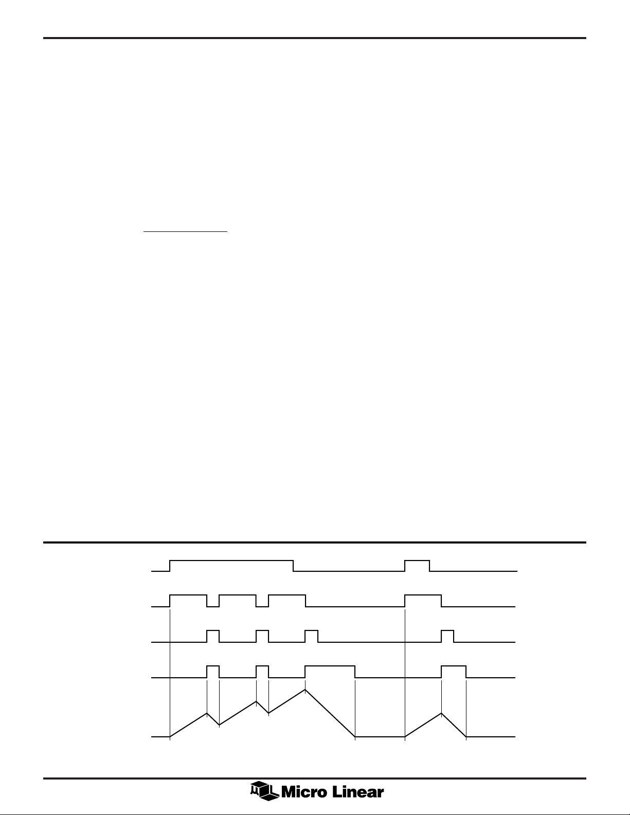
The synchronous rectifier comparator and the two NOR
gates make up the synchronous rectifier control circuit.
The synchronous control does not influence the operation
of the main control loop, and operation with a Schottky
diode in place of the synchronous rectifier is possible, but
at a lower conversion efficiency. The synchronous rectifier
(N DRV) is turned on during the minimum OFF-time or
whenever the I
pin goes below –18mV. N DRV will
SENSE
remain on until a new ON-time is started or until the
I
pin goes above –18mV. When the ISENSE pin goes
SENSE
above –18mV, the current in the inductor has gone to zero
T
OFF(MIN)
V
C
T
ON
V
SR
I
L
Figure 2. One Shot and Synchronous Rectifier Timing Diagram
5
 Loading...