

Micro Linear Corporation ML4877ER, ML4877CR Datasheet
JULY 2000
NEW!
30W CCFL Inverter Design
ML4877*
LCD Desktop Backlight Lamp Driver
GENERAL DESCRIPTION
The ML4877 is an ideal solution for driving multiple cold
cathode fluorescent tubes (CCFL) used in liquid crystal
display (LCD) backlight applications. It provides dimming
ballast control for the LCD display.
By utilizing differential drive the ML4877 can deliver the
same light output with significantly less input power
compared to existing single ended drive schemes.
Improvements as high as 30% can be realized when using
low power lamps and advanced LCD screen housings. This
increased light output is achieved because the differential
drive configuration is much less sensitive, and therefore
less power is wasted in the capacitive parasitics that exist
in the backlight housing. An additional benefit of this
configuration is an even distribution of light.
The IC includes an adjustable lamp out detect circuit that
latches the IC off when a lamp fault is detected. Also, the
unique architecture of the ML4877 allows the
development of a backlight system that will inherently
meet the UL requirements for safety.
The ML4877 is optimized for large LCD applications
applications where high efficiency is critical to maximize
battery life. The high efficiency is achieved by a resonant
scheme with zero voltage switching.
FEATURES
■ Ideal for 30W inverter designs, 1 to 8 lamp design
■ PWM dimming capability
■ Backlight lamp driver with differential drive
■ Up to 30% lower power for same light output
■ Low standby current (<10µA)
■ Improved efficiency (»95%)
■ Allows all N-channel MOSFET drive
■ Adjustable lamp out detect with latch
■ Resonant threshold detection and synchronous
rectification
■ Positive input for dimming control
* THIS PART IS END OF LIFE AS OF JULY 1, 2000
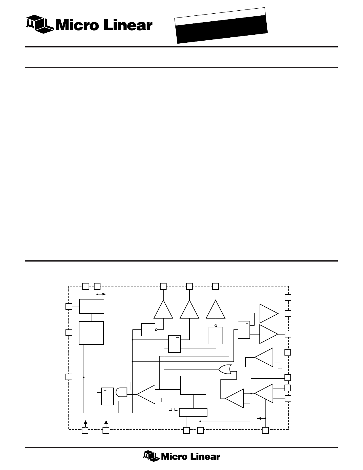
BLOCK DIAGRAM
AZR
2
REGULATOR
5
PGND18GND
LINEAR
MASTER
BIAS
&
UVLO
17
ON/OFF
HVDD
VREF
12
15
VDD
13
VDD
Q
S
QR
B ON
19
DR3 DR1 DR1
ONE
SHOT
SS
+
–
VDD
CLK
S
Q
RQ
B OFF
RESONANT
THRESHOLD
DETECTOR
OSCILLATOR
4
R
T
B SYNC OUT
20
11
L RTD
10
L GATE 1
DR2
Q
NEG
EDGE
DELAY
9
T
T
Q
DR2
–
+
SS
3
SS CAPC
14
L GATE 2
16
6
+
–
–
+
0.5V
8
7
1
L ILIM
LEA OUT
LEA–
LEA+
1
ML4877
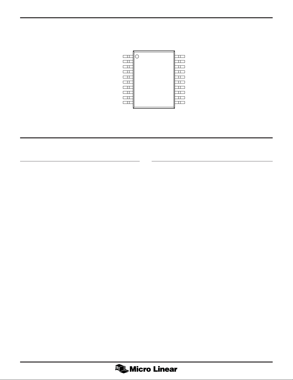
PIN CONFIGURATION
PIN DESCRIPTION
LEA+
AZR
SS CAP
R
VREF
L ILIM
LEA–
LEA OUT
C
L RTD
ML4877
20-Pin SSOP (R20)
1
2
3
T
T
4
5
6
7
8
9
10
TOP VIEW
20
19
18
17
16
15
14
13
12
11
B OFF
B ON
GND
PGND
L GATE 2
ON/OFF
L GATE 1
VDD
HVDD
B SYNC OUT
PIN NAME FUNCTION
1 LEA+ Positive input for lamp error amp
2 AZR Connection to gate of external FET for
high voltage regulator. Internally a
zener diode to ground.
3 SS CAP Connection of optional external soft
start capacitor
4R
T
Oscillator timing resistor
5 VREF Voltage reference output
6 L ILIM Input to current limit amplifier
7 LEA- Negative input for lamp error
amplifier
8 LEA OUT Output of lamp error amplifier.
External compensation capacitor
connects between this pin and LEA.
9C
T
Oscillator timing capacitor
10 L RTD Input to resonant threshold detector
PIN NAME FUNCTION
11 B SYNC Output of MOSFET driver to gate of
OUT synchronous FET catch diode.
12 HVDD Battery power input to linear regulator
13 VDD Output of linear regulator. Positive
power for IC.
14 L GATE1 Output of MOSFET driver. Connection
to gate of one side of inverter FET
drive pair.
15 ON/OFF Logic input for chip
16 L GATE2 Output of MOSFET driver. Connection
to gate of one side of inverter FET
drive pair.
17 PGND Power ground
18 GND Signal ground
19 B ON Connection to primary side of gate
pulse transformer
20 B OFF Output of MOSFET driver. Connection
to gate of FET that disables the input
power.
2
ABSOLUTE MAXIMUM RATINGS
ML4877
Absolute maximum ratings are those values beyond which
the device could be permanently damaged. Absolute
maximum ratings are stress ratings only and functional
device operation is not implied.
Voltage on HVIDD .................................................... 20V
Current into L RTD ............................................... ±10mA
Junction Temperature.............................................. 150ºC
Storage Temperature Range .......................-65ºC to 150ºC
Lead Temperature (Soldering 10 sec.) ..................... 260ºC
Supply Current (ICC) ............................................... 75mA
Thermal Resistance (qJA).................................... 100ºC/W
Output Current, Source or Sink ............................. 250mA
Voltage on Pins LEA+, AZR, SS CAP, RT, VREF,
OPERATING CONDITIONS
L ILIM, LEA-, LEA OUT, CT, B SYNC OUT, VDD,
L GATE 1, ON/OFF, L GATE 2, PGND, GND,
B ON, B OFF ............................... –0.3V to VDD +0.3V
Temperature Range
ML4877C ................................................... 0ºC to 70ºC
ML4877E...............................................–20ºC to 70ºC
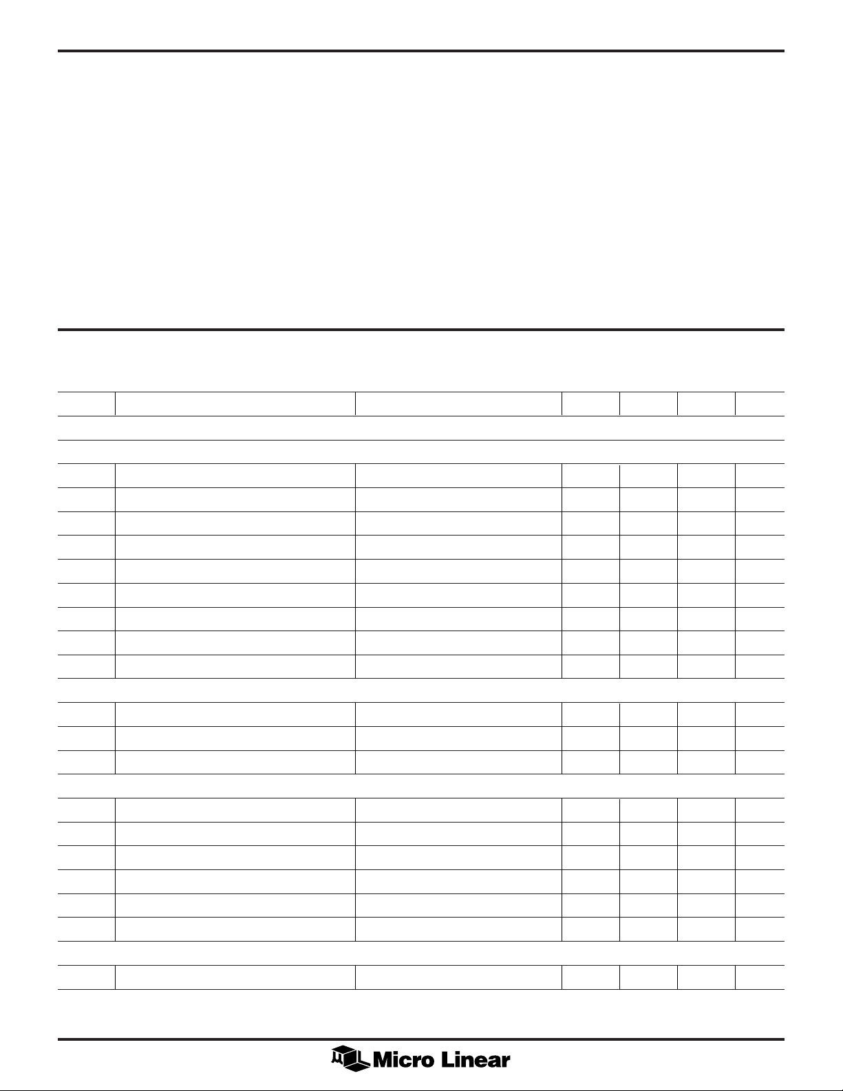
ELECTRICAL CHARACTERISTICS
Unless otherwise specified, VDD = 5V ±5%, TA= Operating Temperature Range, CT = 47pF, RT = 82kW (Note 1)
SYMBOL PARAMETER CONDITIONS MIN TYP MAX UNITS
CURRENT REGULATOR
ERROR AMPLIFIER
Open Loop Gain 60 70 dB
Output High I
Output Low I
Bandwidth (-3dB) 1 MHz
= 5µA 2.8 3.0 V
LOAD
= 25µA 0.4 0.7 V
LOAD
Common Mode Voltage Range 0 1.0 V
Input Bias Current 50 100 nA
Input Offset Voltage -5 0 5 mv
Soft Start Charge Current V
Soft Start Threshold (LEA OUT) V
CURRENT LIMIT COMPARATOR
Current Threshold 450 500 550 mV
Input Bias Current V
Propagation Delay (Note 2) 150 250 ns
OUTPUT DRIVERS
Output High - B SYNC OUT, B OFF VDD 5V, I
Output Low - B SYNC OUT, B OFF I
Rise & Fall time - B SYNC OUT, B OFF C
Output High - B ON VDD 5V, I
Output Low - B ON I
Fall Time - B ON C
ONE SHOT
= 1V 550 750 950 nA
SSCAP
= 1V 2 2.5 V
SSCAP
= 0.1V 50 100 nA
ILIM
= 12mA 4.625 4.8 V
LOAD
12mA 0.2 0.375 V
LOAD
=100pF 20 50 ns
LOAD
= 12mA 4.625 4.8 V
LOAD
50mA 0.2 0.375 V
LOAD
= 2400pF (Note 2) 45 80 ns
LOAD
Pulse Width 100 150 200 ns
3
ML4877
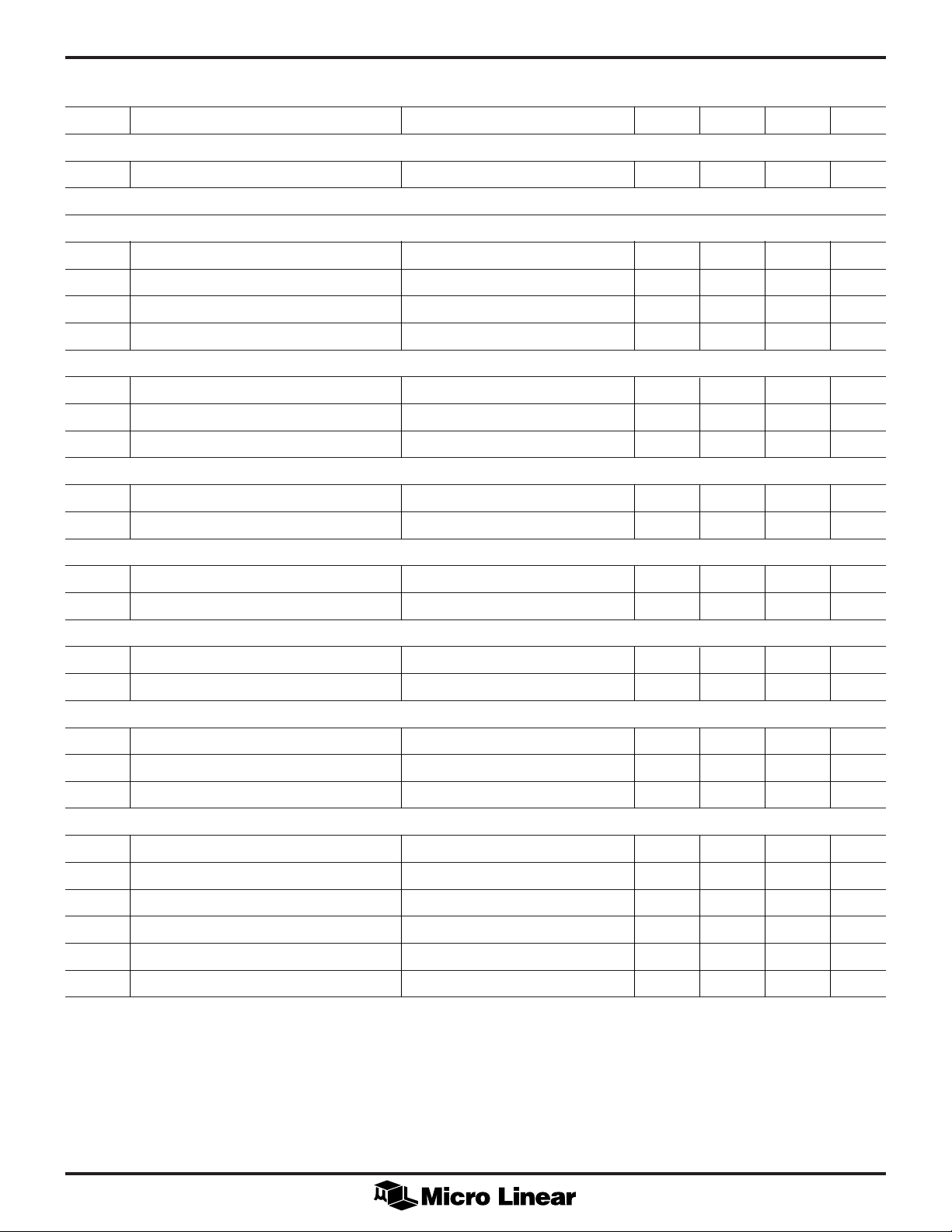
ELECTRICAL CHARACTERISTICS (Continued)
SYMBOL PARAMETER CONDITIONS MIN TYP MAX UNITS
DELAY TIMER
Delay Time 20 35 55 ns
HIGH VOLTAGE INVERTER
Oscillator
Nominal Frequency 68 80 92 kHz
Discharge Current VCT = 2V 500 700 900 µA
Peak Voltage 2.3 2.5 2.7 V
Valley Voltage 0.8 1 1.2 V
Output Drivers
Output High - L GATE 1, 2 VDD = 5V, I
Output Low - L GATE 1, 2 I
Rise & Fall Time - L GATE 1, 2 C
Resonant Threshold Detector
Threshold 0.45 0.8 1.15 V
Hysteresis 0.15 03 0.45 mV
Lamp Out Detect
Threshold -2 VDD 2 %
Latch Inhibit Threshold (SSCAP) LRTD > VDD + 0.1V 2.5 V
Under Voltage Detector
Start Up Threshold 3.8 4.1 4.4 V
Hysteresis 150 300 450 mV
Logic Interface (ON/OFF)
V
IH
V
IL
Input Bias Current ON/OFF = 3V 10 25 µA
Linear Regulator
12mA 4.625 4.8 V
LOAD
= 50mA 0.2 0.375 V
LOAD
=1000pF 20 50 ns
LOAD
2.5 V
0.5 V
Aux Zener Reference Voltage (AZR) I
Regulator Voltage (VDD) HVDD = 12V 4.75 5.0 5.35 V
Regulator Source Current External to device 10 mA
Drop Out Voltage I
Drop Out Voltage l
HVDD Input Voltage Range 5 18 V
= 10µA 12.3 13.5 14.7 V
AZR
= 1mA 30 90 mA
HVDD
= 5mA 125 275 mA
HVDD
4
 Loading...