

Micro Linear Corporation ML4876CR, ML4876ER Datasheet
JULY 2000
FEATURING
Extended Commercial Temperature Range
-20˚C to 70˚C
for Portable Handheld Equipment
ML4876*
LCD Backlight Lamp Driver with Contrast
GENERAL DESCRIPTION
The ML4876 is an ideal solution for driving small cold
cathode fluorescent tubes (CCFL) used in liquid crystal
display (LCD) backlight applications. It provides the
dimming ballast control and the contrast control for the
LCD display.
By utilizing differential drive the ML4876 can deliver the
same light output with significantly less input power
compared to existing single ended drive schemes.
Improvements as high as 30% can be realized when using
low power lamps and advanced LCD screen housings. This
increased light output is achieved because the differential
drive configuration is much less sensitive, and therefore
less power is wasted in the capacitive parasitics that exist
in the backlight housing. An additional benefit of this
configuration is an even distribution of light.
The ML4876 is optimized for portable applications where
high efficiency is critical to maximize battery life. The
high efficiency is achieved by a resonant scheme with
zero voltage switching.
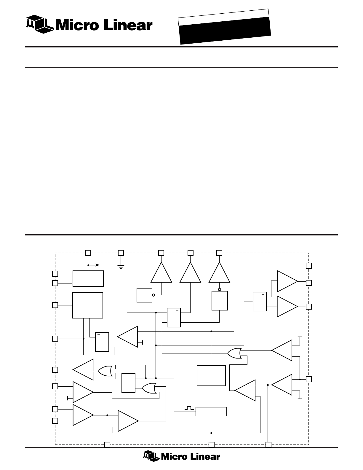
BLOCK DIAGRAM
13 17 18 19 11
HVDD
15
6
ON/OFF
VREF
5
LON
4
F GATE
12
F ILIM
20
0.1V
FEA–
2
FEA+
3
VDD GND
LINEAR
REGULATOR
MASTER
BIAS
&
UVLO
+
–
–
+
VDD
Q
S
QR
Q
QR
–
+
S
+
–
ONE
SHOT
16V
B ON B OFF B SYNC OUT
DR3 DR1 DR1
S
RQ
FEATURES
■ Backlight lamp driver with differential drive
■ Up to 30% lower power for same light output
■ Low standby current (< 10µA)
■ Improved efficiency (»95%)
■ Allows all N-channel MOSFET drive
■ Low switching losses
■ Resonant threshold detection
■ Buck regulator uses synchronous rectification
* THIS PART IS END OF LIFE AS OF JULY 1, 2000
DR2
Q
CLK
NEG
EDGE
DELAY
RESONANT
THRESHOLD
DETECTOR
OSCILLATOR
Q
T
Q
–
+
DR2
L RTD
L GATE 1
L GATE 2
0.5V
–
+
–
LEA–
+
0.2V
10
14
16
7
C
FEA OUT
1 9 8
T
LEA OUT
1
ML4876
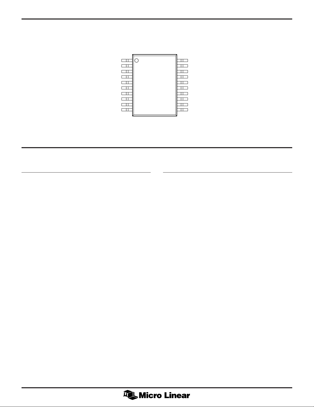
PIN CONFIGURATION
PIN DESCRIPTION
FEA OUT
FEA–
FEA+
L ON
VREF
ON/OFF
LEA–
LEA OUT
C
L RTD
ML4876
20-Pin SSOP (R20)
1
2
3
4
5
6
7
8
T
9
10
TOP VIEW
20
19
18
17
16
15
14
13
12
11
F ILIM
B OFF
B ON
GND
L GATE2
HVDD
L GATE1
VDD
F GATE
B SYNC OUT
PIN NAME DESCRIPTION
1 FEA OUT Output of flyback (contrast) error
amplifier
2 FEA– Negative input of flyback
(contrast) error amplifier
3 FEA+ Positive input of flyback (contrast)
error amplifier
4 L ON Logic input. A ”0“ on this pin
disables the lamp driver section
only
5 VREF Voltage reference output
6 ON/OFF Logic input. A ”0“ on this pin
disables the linear regulator
7 LEA– Negative input for lamp error
amplifier
8 LEAOUT Output of lamp error amplifier
9C
T
Oscillator timing capacitor
10 L RTD Input to resonant threshold detector
PIN NAME DESCRIPTION
11 B SYNC OUT Output of MOSFET driver.
Connects to gate of synchronous
FET catch diode.
12 F GATE Connects to gate of MOSFET in
primary side of contrast control
13 VDD Output of linear regulator. Positive
power for IC.
14 L GATE1 Output of MOSFET driver.
Connection to gate of one side of
inverter FET drive pair
15 HVDD Battery power input to linear
regulator
16 L GATE2 Output of MOSFET driver.
Connection to gate of one side of
inverter FET drive pair
17 GND Ground
18 B ON Connection to primary side of gate
pulse transformer
19 B OFF Output of MOSFET driver.
Connection to gate of FET that
disables the input power.
20 F ILIM Input to current limit comparator
2
ABSOLUTE MAXIMUM RATINGS
ML4876
Absolute maximum ratings are those values beyond which
the device could be permanently damaged. Absolute
maximum ratings are stress ratings only and functional
device operation is not implied.
Voltage on Any Other Pin ............... –0.3V to VDD +0.3V
Junction Temperature ..............................................150°C
Storage Temperature Range ..................... –65°C to 150°C
Lead Temperature (Soldering 10 sec.) .....................260°C
Thermal Resistance (qJA) Plastic SSOP ............... 100°C/W
Supply Current (ICC) ............................................... 75mA
Output Current, Source or Sink ............................. 250mA
OPERATING CONDITIONS
Voltage on HVDD ..................................................... 20V
Current into L RTD ............................................... ±10mA
Transient Voltage on B ON .......................................... 9V
Temperature Range
ML4876C ................................................... 0°C to 70°C
ML4876E ............................................... –20°C to 70°C
ELECTRICAL CHARACTERISTICS
Unless otherwise specified, VDD = 5V ±5%, CT = 47pF, TA = Operating Temperature Range (Note 1)
SYMBOL PARAMETER CONDITIONS MIN TYP MAX UNITS
CURRENT REGULATOR
Error Amplifier
Open Loop Gain 60 70 dB
Bias Point Closed loop 0.18 0.2 0.22 V
Output High I
Output Low I
Bandwidth (–3dB) 1 MHz
= 5µA 2.8 3.0 V
LOAD
= 25µA 0.4 0.7 V
LOAD
Input Voltage Range –0.3 0.2 VREF V
Input Bias Current 50 100 nA
Current Limit Comparator
Current Threshold 450 500 550 mV
Input Bias Current V
Propagation Delay (Note 2) 30 ns
Output Drivers
Output High - B SYNC OUT, B OFF VDD = 5V, I
Output Low - B SYNC OUT, B OFF I
Rise & Fall time - B SYNC OUT, B OFF C
Output High - B ON VDD = 5V, I
Output Low - B ON I
Fall Time - B ON C
ONE SHOT Pulse Width 100 150 200 ns
DELAY TIMER Delay Time 20 35 55 ns
FLYBACK REGULATOR
Error Amplifier
= 0.1V 50 100 nA
LILIM
= 12mA 4.625 4.8 V
LOAD
= 12mA 0.2 0.375 V
LOAD
= 100pF 20 50 ns
LOAD
= 12mA 4.625 4.8 V
LOAD
= 50mA 0.2 0.375 V
LOAD
= 2400pF (Note 2) 45 80 ns
LOAD
Open Loop Gain 60 70 dB
Offset Voltage –15 15 mV
Output High I
Output Low I
= 5µA 2.8 3.0 V
LOAD
= 25µA 0.4 0.7 V
LOAD
3
 Loading...