

Micro Linear Corporation ML4875CS-T, ML4875ES-3, ML4875ES-5, ML4875ES-T, ML4875CS-3 Datasheet
...
July 2000
ML4875*
Low Voltage Boost Regulator with Shutdown
GENERAL DESCRIPTION
The ML4875 is a boost regulator designed for DC to DC
conversion in 1 to 3 cell battery powered systems. The
combination of BiCMOS process technology, internal
synchronous rectification, variable frequency operation,
and low supply current make the ML4875 ideal for 1 cell
applications. The ML4875 is capable of start-up with input
voltages as low as 1V and is available in 5V, 3.3V, and 3V
output versions with an output voltage accuracy of ±3%.
Unlike regulators using external Schottky diodes, the
ML4875 isolates the load from the battery when the
FEATURES
■ Guaranteed start-up and operation at 1V input
■ Pulse Frequency Modulation and Internal Synchronous
Rectification for high efficiency
■ Isolates the load from the input during shutdown
■ Minimum external components
■ Low ON resistance internal switching FETs
■ Micropower operation
■ 5V, 3.3V, and 3V output versions
SHDN pin is high. This is accomplished by an integrated
synchronous rectifier which eliminates the need for an
external Schottky diode and provides a lower forward
voltage drop, resulting in higher conversion efficiency. In
addition, low quiescent battery current and variable
frequency operation result in high efficiency even at light
loads. The ML4875 requires only one inductor and two
capacitors to build a very small regulator circuit capable
of achieving conversion efficiencies in excess of 90%.
The circuit contains a RESET output which goes low when
the DETECT input drops below 200mV. *Some Packages Are End Of Life Or Obsolete
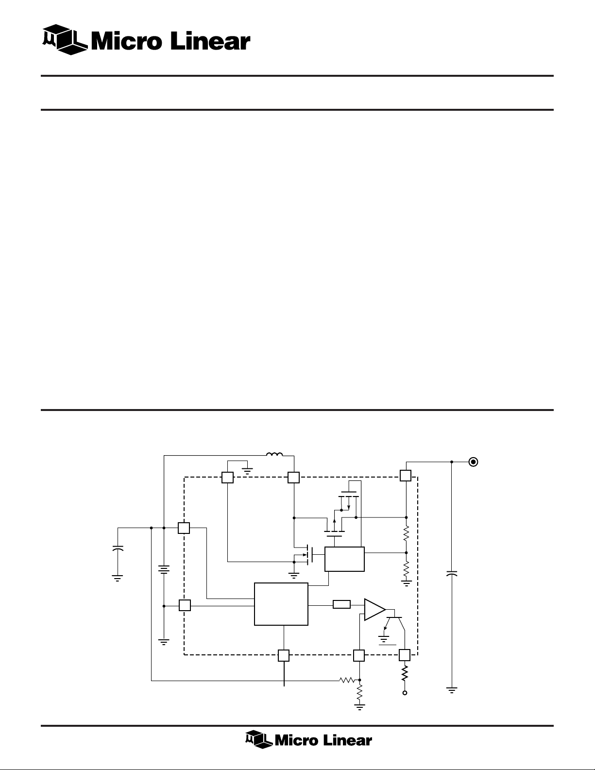
BLOCK DIAGRAM
*C
IN
*Optional
L1
V
C
OUT
OUT
8
PWR
GND
V
IN
1
V
BAT
GND
3
REGULATION
SHUTDOWN
FROM POWER
MANAGEMENT
V
L
&
CONTROL
SHDN
2
6
BOOST
CONTROL
REF
DETECT
FEEDBACK
+
–
4
*R
A
*R
B
V
RESET
5
OUT
7
5V
1
ML4875
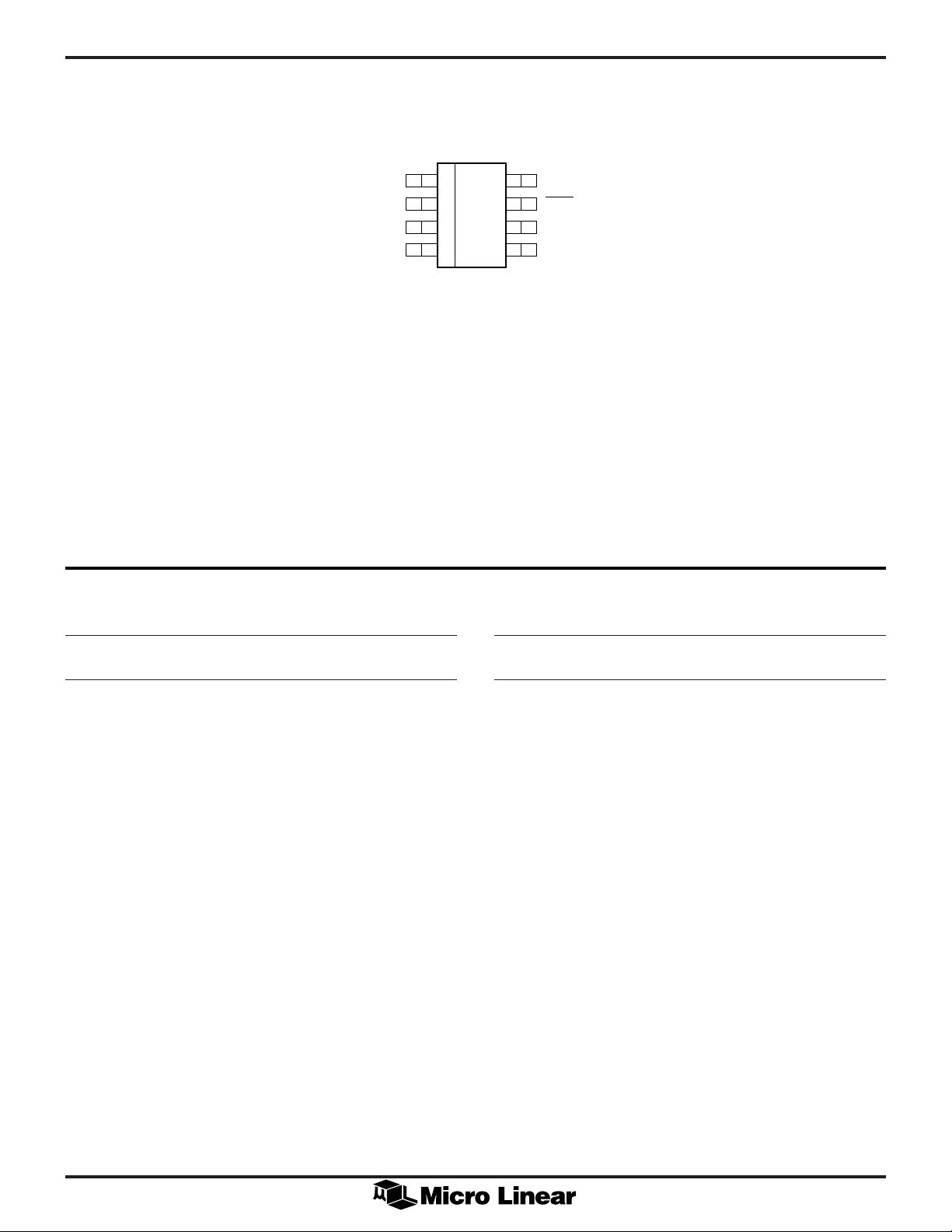
PIN CONNECTION
ML4875-5/-3/-T
8-Pin SOIC (S08)
PIN DESCRIPTION
V
SHDN
GND
DETECT
IN
1
2
3
4
TOP VIEW
8
7
6
5
PWR GND
RESET
V
L
V
OUT
PIN
NO. NAME FUNCTION
1V
IN
Battery input voltage
2 SHDN Pulling this pin high shuts down the
regulator, isolating the load from the
input
3 GND Analog signal ground
4 DETECT When this pin below V
REF
, causes
the RESET pin to go low
PIN
NO. NAME FUNCTION
5V
OUT
6V
L
Boost regulator output
Boost inductor connection
7 RESET Output goes low when regulation
cannot be achieved or when DETECT
goes below 200mV
8 PWR GND Return for the NMOS output transistor
2
ML4875
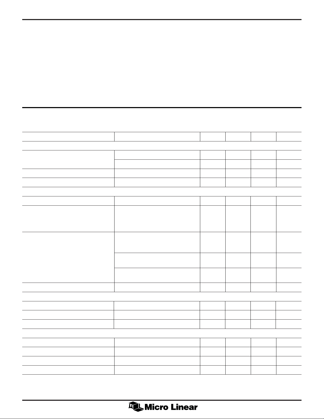
ABSOLUTE MAXIMUM RATINGS
Lead Temperature (Soldering 10 sec.) ..................... 260°C
Thermal Resistance (qJA) Plastic SOIC ................. 160°C/W
Absolute maximum ratings are those values beyond which
the device could be permanently damaged. Absolute
maximum ratings are stress ratings only and functional
device operation is not implied.
V
................................................................................................ 7V
OUT
Voltage on any other pin ......GND – 0.3V to V
Peak Switch Current, I
Average Switch Current, I
................................................. 1.5A
(PEAK)
....................................... 300mA
(AVG)
OUT
+ 0.3V
Junction Temperature ............................................. 150°C
OPERATING CONDITIONS
Temperature Range
ML4875CS-X ..............................................0°C to 70°C
ML4875ES-X ........................................... –20°C to 70°C
V
Operating Range
IN
ML4875CS-X ................................. 1.0V to V
ML4875ES-X .................................. 1.1V to V
OUT
OUT
–0.2V
–0.2V
Storage Temperature Range ...................... –65°C to 150°C
ELECTRICAL CHARACTERISTICS
Unless otherwise specified, V
PARAMETER CONDITIONS MIN TYP. MAX UNITS
SUPPLY
VIN Current VIN = V
V
Quiescent Current 812µA
OUT
V
Quiescent Current 1µA
L
PFM REGULATOR
= Operating Voltage Range, TA = Operating Temperature Range (Note 1).
IN
– 0.2V 50 65 µA
OUT
VIN = 4.8V, SHDN = V
IN
20 30 µA
Pulse Width (TON) 8.9 10 11.1 µs
Output Voltage (V
ML4875-5 T
ML4875-3 8.9µs - T
ML4875-T 2.91 3.0 3.09 V
Load Regulation See Figure 1
ML4875-5 V
ML4875-3 V
ML4875-T V
Under-Voltage Lockout Threshold 0.85 1 V
SHUTDOWN
Input Bias Current –100 100 nA
Shutdown Threshold V
Shutdown Hysteresis 50 70 mV
RESET COMPARATOR
DETECT Threshold 194 200 206 mV
DETECT Bias Current –100 100 nA
OUT
)
= 0 at V
ON
= 1.2V, I
IN
VIN = 2.4V, I
= 1.2V, I
IN
VIN = 2.4V, I
= 1.2V, I
IN
VIN = 2.4V, I
= high to low 180 200 220 mV
SHDN
(MAX), 4.85 5.0 5.15 V
OUT
- 11.1µs V
ON
OUT
OUT
OUT
OUT
OUT
OUT
- 20mA 4.85 5.0 5.15 V
- 100mA 4.85 5.0 5.15 V
- 30mA 3.2 3.3 3.4 V
- 140mA 3.2 3.3 3.4 V
- 35mA 2.91 3.0 3.09 V
- 160mA 2.91 3.0 3.09 V
(MIN) 3.2 3.3 3.4 V
OUT
RESET ON Voltage I
RESET OFF Current V
Note 1: Limits are guaranteed by 100% testing, sampling or correlation with worst case test conditions.
= 50µA 100 200 mV
RESET
= 5V 1 µA
RESET
3
 Loading...