

Micro Linear Corporation ML4866ES, ML4866IS, ML4866CS Datasheet
July 2000
ML4866*
3.3V Output DC–DC Step-Down Converter
GENERAL DESCRIPTION
The ML4866 is a high efficiency pulse width modulated
(PWM) buck regulator designed for use in 5V systems or
portable equipment that need a compact, efficienct 3.3V
supply. It has a switching frequency of 120kHz and uses
synchronous rectification to optimize power conversion
efficiency. Unlike other solutions, the ML4866 requires no
external diodes or FETs.
The ML4866 can provide up to 500mA of output current,
and operates over an input voltage range of 3.5V to 6.5V
(3 to 4 cells or a 5 VDC supply). A complete switched
mode power converter can be quickly and easily
implemented with few external components. Thanks to a
built-in autoburst mode, power conversion efficiency of
this DC–DC converter can exceed 90% over more than 2
decades of output load current.
Stability and fast loop response are provided by current
programming and a current sense circuit. The ML4866
also has a SHDN pin for use in systems which have power
management control. Undervoltage lockout and soft start
are also built in.
FEATURES
■ High power conversion efficiency over 2 decades of
load current
■ No external FETs or diodes; minimum external
components
■ 3.5V to 6.5V input voltage range
■ Significantly extends battery life over linear regulator
based solutions
■ Micropower operation
■ Low shutdown mode quiescent current
(* Indicates Part is End Of Life as of July 1, 2000)
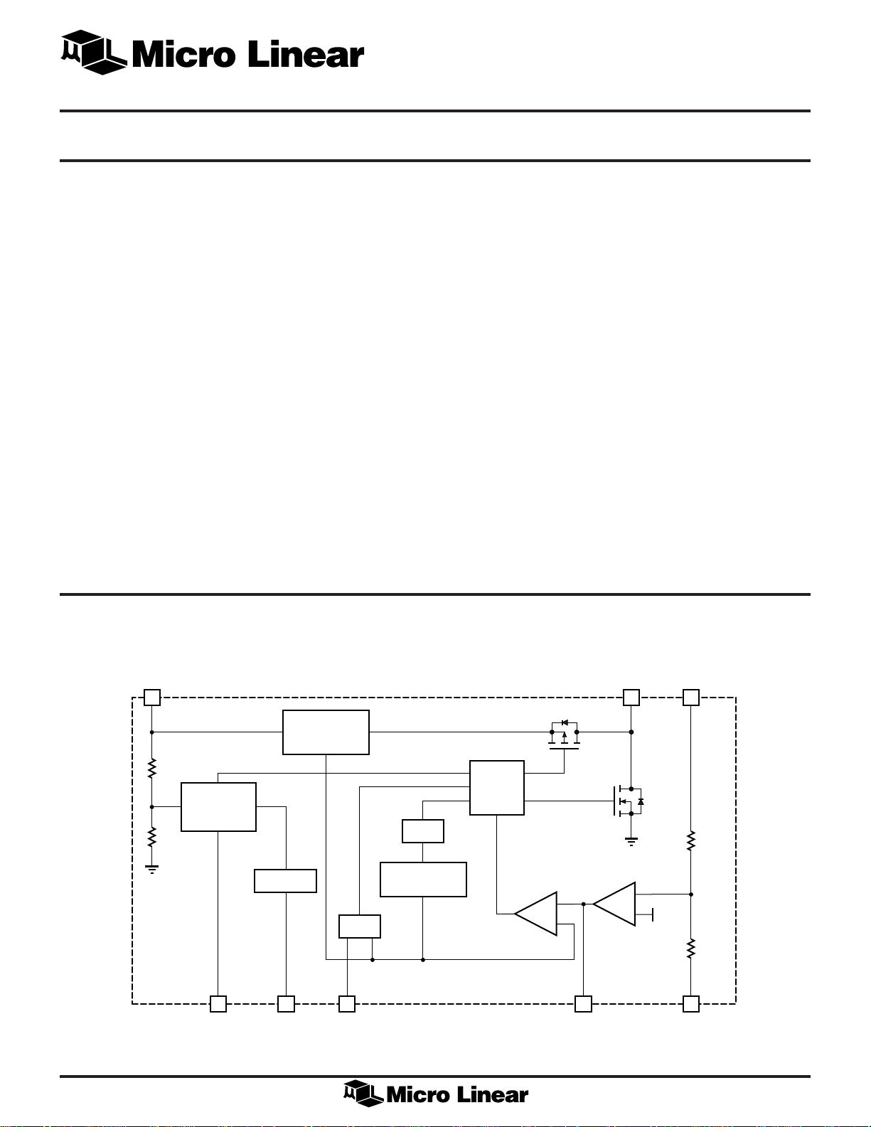
BLOCK DIAGRAM
5
V
IN
UVLO/
SHUTDOWN
6
SHDN
REFERENCE
V
3
CURRENT
SENSE
REF
BURST
BURST
4
OSC
SLOPE
COMPENSATION
BUCK
CONTROL
–
+
ERROR
AMPLIFIER
COMP
2
7
V
–
+
1
V
L
V
REF
OUT
GND
8
1

ML4866
PIN CONFIGURATION
ML4866
8-Pin SOIC (S08)
V
OUT
COMP
V
REF
BURST
PIN DESCRIPTION
PIN NAME FUNCTION
1V
OUT
2 COMP Connection point for an external
Regulated 3.3V output
compensation network
1
2
3
4
TOP VIEW
8
7
6
5
PIN NAME FUNCTION
5V
IN
GND
V
L
SHDN
V
IN
Input voltage
6 SHDN Pulling this pin low shuts down the
regulator
3V
REF
1.25V reference output
4 BURST This pin controls when the control
circuit switches between PWM and
PFM modes of operation
7V
L
Buck inductor connection
8 GND Ground
2

ML4866
ABSOLUTE MAXIMUM RATINGS
Absolute maximum ratings are those values beyond which
the device could be permanently damaged. Absolute
maximum ratings are stress ratings only and functional
device operation is not implied.
OPERATING CONDITIONS
Temperature Range
ML4866CS ................................................. 0ºC to 70ºC
ML4866ES .............................................. -20ºC to 70ºC
ML4866IS ............................................... -40ºC to 85ºC
VIN Operating Range ...................................3.5V to 6.5V
V
................................................................................................... 7V
IN
Voltage on any other pin .........GND - 0.3V to VIN + 0.3V
Peak Switch Current (I
Average Switch Current (I
) ......................................... 2A
PEAK
).....................................1A
AVG
Junction Temperature.............................................. 150ºC
Storage Temperature Range ....................... -65ºC to 150ºC
Lead Temperature (Soldering 10 Sec.)..................... 260ºC
Thermal Resistance (qJA).................................... 160ºC/W
ELECTRICAL CHARACTERISTICS
Unless otherwise specified, VIN = 5V, L = 50µH, C
TA = Operating Temperature Range (Note 1)
SYMBOL PARAMETER CONDITIONS MIN TYP MAX UNITS
REFERENCE
V
REF
PWM REGULATOR
Output Voltage 0 < I(V
= 100µF, R
OUT
) < –5µA, I
REF
COMP
OUT
= 390kW, C
= 0mA 1.22 1.25 1.27 V
COMP
= 15nF,
f
OSC
SHUTDOWN
Oscillator Initial Accuracy I
Oscillator Total Variation Line and Temp 90 130 185 kHz
Soft Start VIN to V
BURST Burst Mode Threshold 250 400 mV
BURST PWM Mode Threshold 500 850 mV
BURST Bias Current 35 µA
Output Voltage I
Line Regulation VIN = 4V to 6.5V, TA = 25°C ±2 %
Load Regulation I
Temperature Stability TA = -40°C to 85°C ±1 %
Total Variation Line, Load, Temp ±5 %
UVLO Startup Threshold 3.2 3.5 V
UVLO Shutdown Threshold 2.9 3.1 V
Delay 3 5 ms
OUT
= 200mA, TA = 25°C 100 115 165 kHz
OUT
= 200mA 3.2 3.3 3.4 V
OUT
I
= 20mA, BURST = 0V 3.28 3.38 3.48 V
OUT
= 100mA to 500mA, ±2.5 %
OUT
TA = 25°C
I
= 5mA to 100mA, ±2.5 %
OUT
BURST = 0V, TA = 25°C
SHDN Threshold 2V
SHDN Bias Current –5 µA
3
 Loading...