

Micro Linear Corporation ML4833CS, ML4833CP Datasheet
July 2000
PRELIMINARY
ML4833*
Electronic Dimming Ballast Controller
GENERAL DESCRIPTION
The ML4833 is a complete solution for a dimmable or a
non-dimmable, high power factor, high efficiency
electronic ballast. The BiCMOS ML4833 contains
controllers for “boost” type power factor correction as
well as for a dimming ballast. The ML4833 was designed
to minimize the number of external components required
to build an electronic ballast.
The PFC circuit uses a new, simple PFC topology which
requires only one loop for compensation. This system
produces a power factor of better than 0.99 with low
input current THD. An overvoltage protection comparator
inhibits the PFC section in the event of a lamp out or lamp
failure condition.
The ballast controller section provides for programmable
starting sequence with individually adjustable preheat and
lamp out-of-socket interrupt times. The IC controls lamp
output power through feedback. The ML4833 provides a
power down input which reduces power to the lamp, for
GFI, end of life, etc.
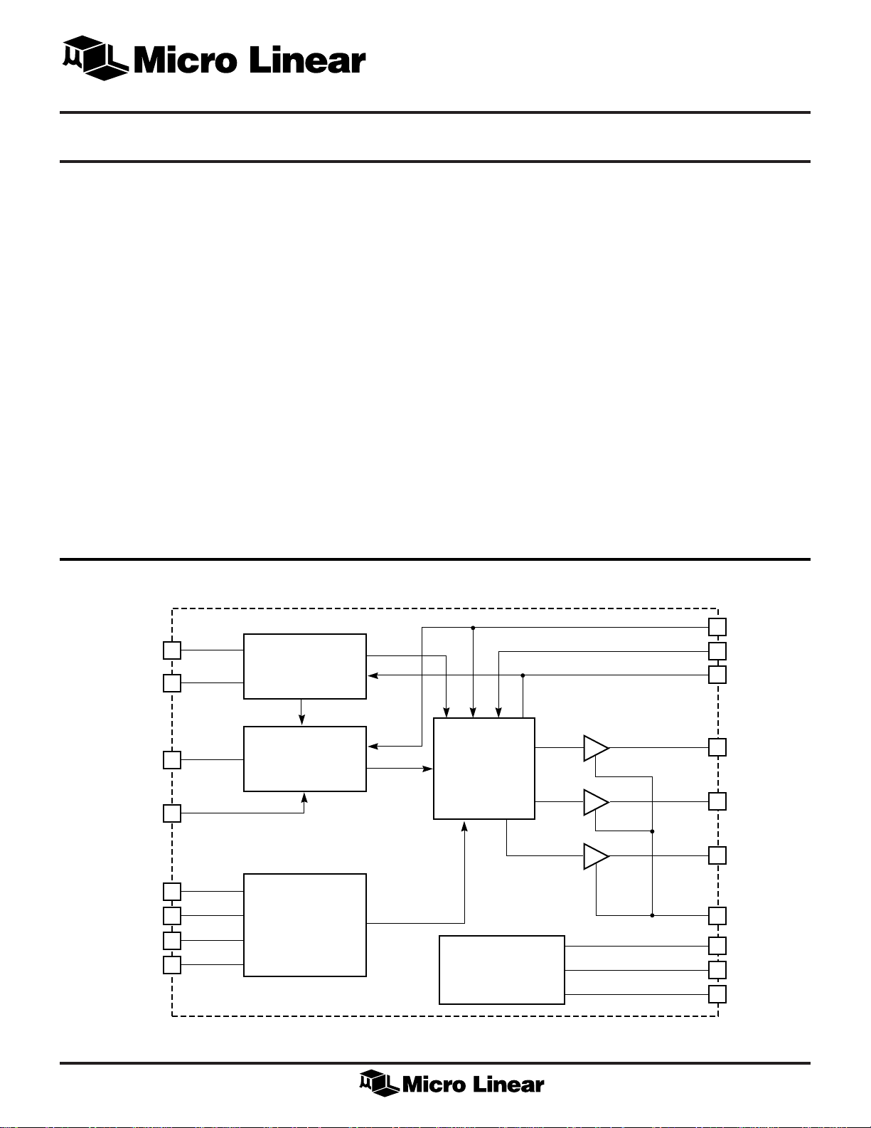
BLOCK DIAGRAM
FEATURES
■ Complete power factor correction and dimming
ballast control in one IC
■ Low distortion, high efficiency continuous boost,
peak current sensing PFC section
■ Programmable start scenario for rapid or
instant start lamps
■ Lamp current feedback for dimming control
■ Variable frequency dimming and starting
■ Programmable restart for lamp out condition to
reduce ballast heating
■ Internal over-temperature shutdown replaces
external heat sensor
■ PFC overvoltage comparator eliminates output
“runaway” due to load removal
■ Low start-up current <0.5mA
■ Power reduction pin for end of life and GFI detectors
(* Indicates part is End Of Life as of July 1, 2000)
6
7
9
3
10
2
1
18
R
SET
/CT
R
T
R
X/CX
PDWN
C
RAMP
PIFB
PEAO
PVFB/OVP
VARIABLE FREQUENCY
OSCILLATOR
PRE-HEAT
AND INTERRUPT
TIMERS
POWER
FACTOR
CONTROLLER
CONTROL
&
GATING LOGIC
UNDER-VOLTAGE
AND THERMAL
SHUTDOWN
OUTPUT
DRIVERS
INTERRUPT
LAMP FB
LFB OUT
OUT A
OUT B
PFC OUT
PGND
VCC
V
REF
GND
8
4
5
14
13
15
12
16
17
11
1
ML4833
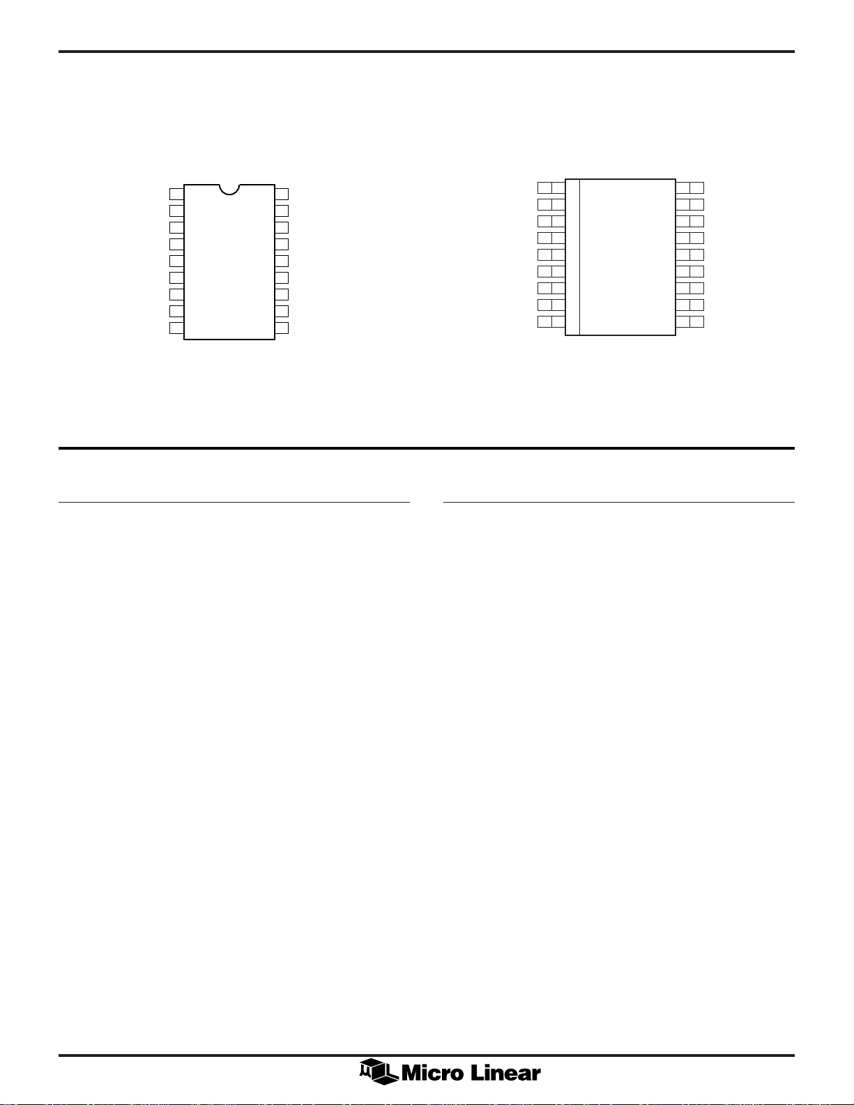
PIN CONFIGURATION
PEAO
PIFB
PDWN
LAMP FB
LFB OUT
R
SET
RT/C
INTERRUPT
R
X/CX
ML4833
18-Pin DIP (P18)
1
2
3
4
5
6
7
T
8
9
TOP VIEW
18
17
16
15
14
13
12
11
10
PVFB/OVP
V
REF
VCC
PFC OUT
OUT A
OUT B
P GND
GND
C
RAMP
PEAO
PIFB
PDWN
LAMP FB
LFB OUT
R
SET
RT/C
INTERRUPT
R
X/CX
T
ML4833
18-Pin SOIC (S18)
1
2
3
4
5
6
7
8
9
TOP VIEW
PIN DESCRIPTION
PIN# NAME FUNCTION PIN# NAME FUNCTION
1 PEAO PFC error amplifier output and
compensation node.
2 PIFB Sensing of the inductor current and
peak current sense point of the PFC
cycle by cycle current limit
comparator.
3 PDWN A one volt comparator threshold that
switches the operating frequency to
the preheat frequency when exceeded.
4 LAMP FB Inverting input of an error amplifier
used to sense (and regulate) lamp arc
current. Also the input node for
dimming control.
5 LFB OUT Output of the lamp current error
transconductance amplifier used for
lamp current loop compensation.
6R
SET
7RT/C
T
External resistor which sets oscillator
F
, and R(X)/C(X) charging current.
MAX
Oscillator timing components.
8 INTERRUPT Input used for lamp-out detection and
restart. A voltage less than 1.25 volts
resets the chip and causes a restart
after a programmable interval.
9RX/C
X
Sets the timing for the preheat,
dimming lockout, and interrupt.
10 C
RAMP
Integrated voltage of the error
amp out.
11 GND Ground.
12 P GND Power ground for the IC.
13 OUT B Ballast MOSFET drive output.
14 OUT A Ballast MOSFET drive output.
15 PFC OUT Power Factor MOSFET drive output.
16 VCC Positive supply for the IC.
17 V
REF
Buffered output for the 7.5V voltage
reference.
18 PVFB/OVP Inverting input to PFC error amplifier
and OVP comparator input.
18
17
16
15
14
13
12
11
10
PVFB/OVP
V
REF
VCC
PFC OUT
OUT A
OUT B
P GND
GND
C
RAMP
2
ML4833
ABSOLUTE MAXIMUM RATINGS
Maximum Forced Voltage
(PEAO, LFB OUT) ...................................–0.3V to 7.7V
Absolute maximum ratings are those values beyond which
the device could be permanently damaged. Absolute
maximum ratings are stress ratings only and functional
device operation is not implied.
Supply Current (ICC) ............................................... 60mA
Output Current, Source or Sink
(OUT A, OUT B, PFC OUT) DC ......................... 250mA
Maximum Forced Current (PEAO, LFB OUT) ........ ±20mA
Junction Temperature ............................................ 150°C
Storage Temperature Range ..................... –65°C to 150°C
Lead Temperature (Soldering 10 sec.) .................... 260°C
Thermal Resistance (qJA)
ML4833CP ...................................................... 70°C/W
ML4833CS .................................................... 100°C/W
Output Energy (capacitive load per cycle).............. 1.5 mJ
Analog Inputs
OPERATING CONDITIONS
(LAMP FB, INTERRUPT, VCC) ........... –0.3V to VCC –2V
PIFB input voltage .........................................–1.5V to 2V
Temperature Range ........................................0°C to 85°C
ELECTRICAL CHARACTERISTICS
Unless otherwise specified, R
PARAMETER CONDITIONS MIN TYP MAX UNITS
Lamp Current Amplifier (LAMP FB, LFB OUT)
Input Bias Current –0.3 –1.0 µA
Small Signal Transconductance 35 65 105 µW
Input Voltage Range –0.3 5.0 V
Output Low Voltage at LAMP FB = 3V, RL = 0.2 0.4 V
Output High Voltage at LAMP FB = 2V, RL = 7.1 7.5 7.8 V
Source Current Voltage at LAMP FB = 0V,
Sink Current Voltage at LAMP FB = 5V,
PFC Voltage Feedback Amplifier (PEAO, PVFB/OVP)
Input Bias Current –0.3 –1.0 µA
Small Signal Transconductance 35 65 105 µW
Input Voltage Range –0.3 5.0 V
Output Low Voltage at PVFB = 3V, RL = 0.2 0.4 V
Output High Voltage at PVFB = 2V, RL = 6.5 6.8 7.1 V
Source Current Voltage at PVFB/OVP = 0V,
Sink Current Voltage at PVFB/OVP = 3V,
PFC Current — Limit Comparator (PIFB)
Current-Limit Threshold –0.90 –1.05 –1.15 V
Propagation Delay 100mV step and 100mV overdrive 100 ns
Oscillator
Initial Accuracy TA = 25°C 72 76 80 kHz
Voltage Stability V
Temperature Stability 2%
Total Variation Line, temperature 69 83 kHz
Ramp Valley to Peak 2.5 V
= 22.1ký, RT = 15.8kW, CT = 1.5nF, C
SET
LFB OUT = 7V, TA = 25°C –0.05 –0.15 –0.25 mA
LFB OUT = 0.3V, TA = 25°C 0.05 0.12 0.22 mA
PEAO = 6V, TA = 25°C –0.05 –0.15 –0.25 mA
PEAO = 0.3V, TA = 25°C 0.03 0.07 0.16 mA
– 4.5V < VCC <V
CCZ
= 1µF, VCC = 12.5V. (Note 1)
VCC
– 0.5V 1 %
CCZ
W
W
3
ML4833
ELECTRICAL CHARACTERISTICS (Continued)
PARAMETER CONDITIONS MIN TYP MAX UNITS
Oscillator (Continued)
C
Charging Current Voltage at LAMP FB = 3V,
T
CT Discharge Current Voltage at RT/CT = 2.5V 4.0 5.5 7.0 mA
Output Drive Deadtime 0.65 1 1.35 µs
Reference Section
Output Voltage TA = 25°C, IO = 1mA 7.4 7.5 7.6 V
Line regulation V
Load regulation 1mA < IO < 5mA 2 15 mV
Temperature stability 0.4 %
Total Variation Line, load, temp 7.35 7.65 V
Output Noise Voltage 10Hz to 10kHz 50 µV
Long Term Stability TJ = 125°C, 1000 hrs 5 mV
Preheat and Interrupt Timer (RX/CX where RX = 680ký, CX = 4.7µF)
Initial Preheat Period 0.8 s
Subsequent Preheat Period 0.7 s
Start Period 1.2 s
Interrupt Period 5.7 s
RX/CX Charging Current –24 –28 –33 µA
RX/CX Open Circuit Voltage VCC < Start-up threshold 0.4 0.7 1.0 V
RX/CX Maximum Voltage 7.0 7.3 7.7 V
Input Bias Current Voltage at C
Preheat Lower Threshold 1.05 1.22 1.36 V
Preheat Upper Threshold 4.2 4.7 5.1 V
Interrupt Recovery Threshold 1.05 1.22 1.36 V
Start Period End Threshold 6.05 6.6 7.35 V
Interrupt Input (INTERRUPT)
Interrupt Threshold 1.1 1.22 1.4 V
Input Bias Current 0.1 µA
R
Voltage 2.4 2.5 2.6 V
SET
OVP Comparator (PVFB/OVP)
OVP Threshold 2.63 2.73 2.83 V
Hysteresis 0.18 0.23 0.27 V
Propagation Delay 1.4 µs
RT/CT = 2.5V, RX/CX = 0.9V (Preheat) –90 –110 –130 µA
LAMP FB = 3V, R
RX/CX = Open –180 –220 –260 µA
– 4.5V < VCC < V
CCZ
RAMP
= 2.5V,
T/CT
– 0.5V 2 35 mV
CCZ
= 1.2V 0.1 µA
4
 Loading...