

Micro Linear Corporation ML4832CP, ML4832CS Datasheet
July 2000
PRELIMINARY
ML4832*
Electronic Dimming Ballast Controller
GENERAL DESCRIPTION
The ML4832 is a complete solution for a dimmable/nondimmable, high power factor, high efficiency electronic
ballast. The BiCMOS ML4832 contains controllers for
“boost” type power factor correction as well as for a
dimming ballast.
The power factor circuit uses the average current sensing
method with a gain modulator and overvoltage protection.
This system produces a power factor of better than 0.99
with low input current THD at > 95% efficiency. Special
care has been taken in the design of the ML4832 to
increase system noise immunity by using a high amplitude
oscillator, and a current-fed multiplier. An overvoltage
protection comparator inhibits the PFC section in the
event of a lamp out or lamp failure condition.
The ballast section provides for programmable starting
scenarios with programmable preheat and lamp out-ofsocket interrupt times. The IC controls lamp output through
frequency modulation using lamp current feedback.
FEATURES
■ Complete power factor correction and dimming
ballast control in one IC
■ Low distortion, high efficiency continuous boost,
average current sensing PFC section
■ Programmable start scenario for rapid or instant
start lamps
■ Lamp current feedback for dimming control
■ Variable frequency dimming and starting
■ Programmable restart for lamp out condition to
reduce ballast heating
■ Over-temperature shutdown replaces external
heat sensor for safety
■ PFC overvoltage comparator eliminates output
“runaway” due to load removal
■ Large oscillator amplitude and gain modulator
improves noise immunity
■ Low start-up current <0.5mA
(* Indicates part is End Of Life as of July 1, 2000)
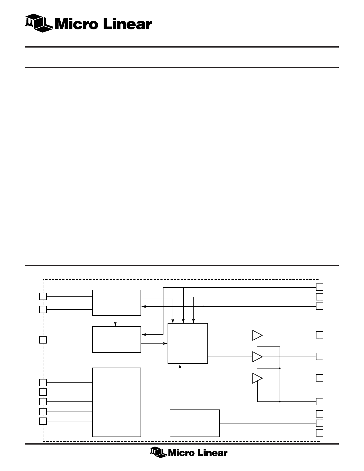
BLOCK DIAGRAM
R
SET
7
R
T/CT
8
R
X/CX
10
IA OUT
2
IA+
4
I
SINE
3
EA OUT
1
EA–/OVP
18
VARIABLE FREQUENCY
OSCILLATOR
PRE-HEAT
AND INTERRUPT
TIMERS
POWER
FACTOR
CONTROLLER
CONTROL
&
GATING LOGIC
UNDER-VOLTAGE
AND THERMAL
SHUTDOWN
OUTPUT
DRIVERS
INTERRUPT
LAMP FB
LFB OUT
OUT A
OUT B
PFC OUT
PGND
V
V
REF
GND
9
5
6
14
13
15
12
CC
16
17
11
1
ML4832
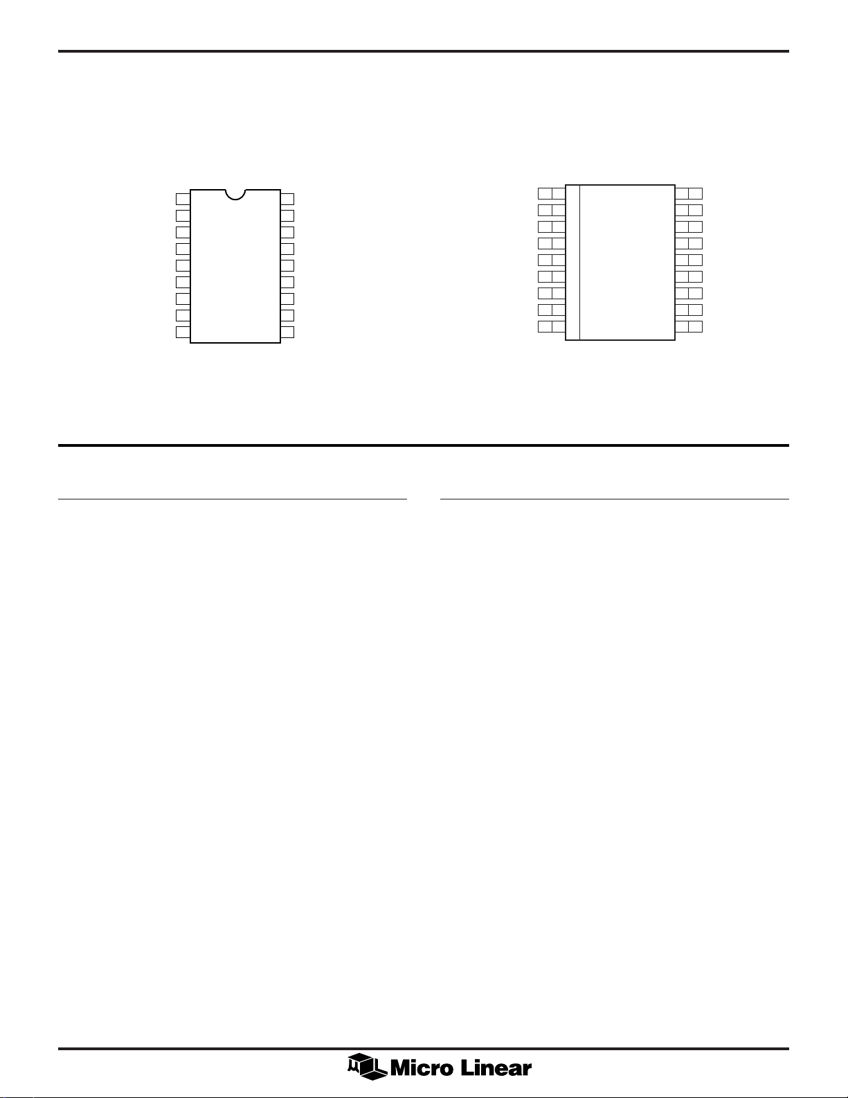
PIN CONFIGURATION
ML4832
18-Pin SOIC (S18)
1
2
3
4
5
6
7
8
9
TOP VIEW
EA OUT
IA OUT
I
SINE
IA+
LAMP FB
LFB OUT
R
SET
RT/C
INTERRUPT
ML4832
18-Pin DIP (P18)
1
2
3
4
5
6
7
8
T
9
TOP VIEW
18
EA–/OVP
17
V
REF
V
16
CC
PFC OUT
15
OUT A
14
OUT B
13
P GND
12
GND
11
R
10
X/CX
EA OUT
IA OUT
I
SINE
IA+
LAMP FB
LFB OUT
R
SET
RT/C
INTERRUPT
T
PIN DESCRIPTION
PIN# NAME FUNCTION PIN# NAME FUNCTION
1 EA OUT PFC error amplifier output and
compensation node
2 IA OUT Output and compensation node of the
PFC average current transconductance
amplifier
3I
SINE
PFC gain modulator input
9 INTERRUPT Input used for lamp-out detection
and restart. A voltage greater than
7.5 volts resets the chip and
causes a restart after a
programmable interval.
10 RX/C
X
Sets the timing for the preheat,
dimming lockout, and interrupt
18
17
16
15
14
13
12
11
10
EA–/OVP
V
REF
V
CC
PFC OUT
OUT A
OUT B
P GND
GND
R
X/CX
4 IA+ Non-inverting input of the PFC average
current transconductance amplifier
and peak current sense point of the
PFC cycle by cycle current limit
comparator
5 LAMP FB Inverting input of an error amplifier
used to sense (and regulate) lamp arc
current. Also the input node for
dimming control.
6 LFB OUT Output from the lamp current error
transconductance amplifier used for
lamp current loop compensation
7R
SET
8RT/C
T
External resistor which sets oscillator
F
, and RX/CX charging current
MAX
Oscillator timing components
11 GND Ground
12 P GND Power ground for the IC
13 OUT B Ballast MOSFET drive output
14 OUT A Ballast MOSFET drive output
15 PFC OUT Power Factor MOSFET drive
output
16 V
17 V
CC
REF
Positive supply for the IC
Buffered output for the 7.5V
voltage reference
18 EA–/OVP Inverting input to PFC error
amplifier and OVP comparator
input
2
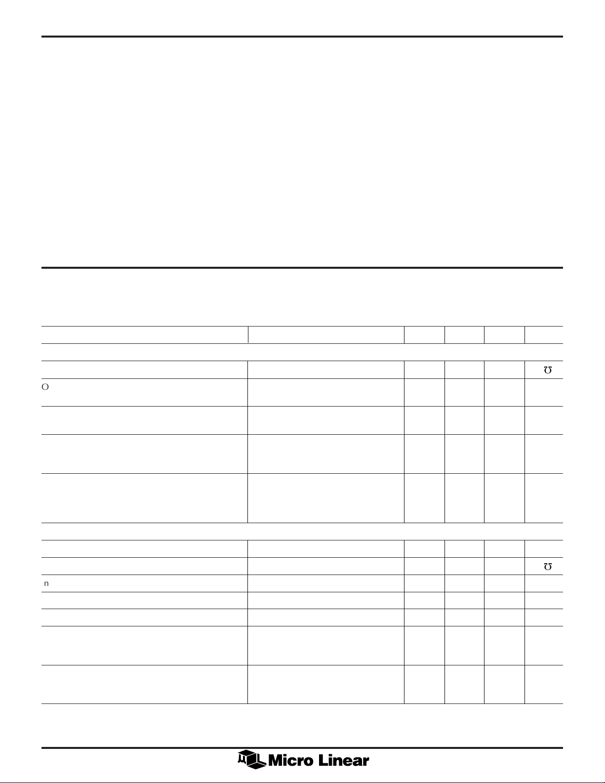
ABSOLUTE MAXIMUM RATINGS
ML4832
Absolute maximum ratings are those values beyond which
the device could be permanently damaged. Absolute
maximum ratings are stress ratings only and functional
device operation is not implied.
Maximum Forced Voltage
(IA OUT)................................................. –0.3V to 7.5V
Junction Temperature ............................................. 150°C
Storage Temperature Range...................... –65°C to 150°C
Lead Temperature (Soldering 10 sec.) ..................... 260°C
Supply Current (ICC) ............................................... 60mA
Output Current, Source or Sink (OUT A, OUT B, PFC
OUT)
Thermal Resistance (qJA)
Plastic PDIP ..................................................... 70°C/W
Plastic SOIC................................................... 100°C/W
DC ................................................................... 250mA
Output Energy (capacitive load per cycle)............... 1.5mJ
Gain Modulator I
Input .....................................10mA
SINE
Analog Inputs ....................................... –0.3V to VCC –2V
IA+ Input Voltage.............................................. –3V to 2V
OPERATING CONDITIONS
Temperature Range
ML4832C ..................................................0°C to 85°C
Maximum Forced Voltage
(EA OUT, LFB OUT) ................................ –0.3V to 7.7V
Maximum Forced Current
(EA OUT, IA OUT, LFB OUT) ............................±20mA
ELECTRICAL CHARACTERISTICS
Unless otherwise specified, R
TA = Operating Temperature Range (Note 1)
PARAMETER CONDITIONS MIN TYP MAX UNITS
PFC CURRENT SENSE AMPLIFIER
Small Signal Transconductance 40 90 120 µ
= 22.1kW, RT = 15.8kW, CT = 1.5nF, C(VCC) = 1µF, I
SET
= 200µA, VCC = 12.5V,
SINE
W
Output Low I
Output High I
Source Current I
Sink Current I
PFC VOLTAGE FEEDBACK AMPLIFIER/LAMP CURRENT AMPLIFIER
Input Bias Current –0.3 –1.0 µA
Small Signal Transconductance 30 55 90 µ
Input Voltage Range –0.3 5.0 V
Output Low V
Output High V
Source Current V
= 0mA, V
SINE
V
= –0.3V, RL = ¥ 0.2 0.4 V
IA+
= 1.5mA, 6.3 6.8 V
SINE
V
SINE
V
V
SINE
V
V
TJ = 25ºC 0.03 0.07 0.16 mA
V
TJ = 25ºC
= V
EA–/OVP
= 1.5mA, –0.05 –0.15 –0.25 mA
EA–/OVP
IA OUT
= 0mA, V
= –0.6V
IA+
EA OUT
LAMP FB
LAMP FB
LAMP FB
EA OUT
IA+
= V
IA+
= 6V, TJ = 25ºC
= 0V, V
= V
EA–/OVP
= V
EA–/OVP
= V
EA–/OVP
= V
LFB OUT
= 0V,
EA OUT
= 0V, RL = ¥
= 0V,
= 0.3V,
IA OUT
= 5V,
EA–/OVP
= 3V, RL = ¥ 0.2 0.4 V
= 2V, RL = ¥ 7.1 7.5 7.8 V
= 0V, –0.06 –0.15 –0.30 mA
= 7V,
W
Sink Current V
LAMP FB
V
EA OUT
TJ = 25ºC
= V
= V
EA–/OVP
LFB OUT
= 5V, 0.06 0.12 0.28 mA
= 0.3V,
3
ML4832
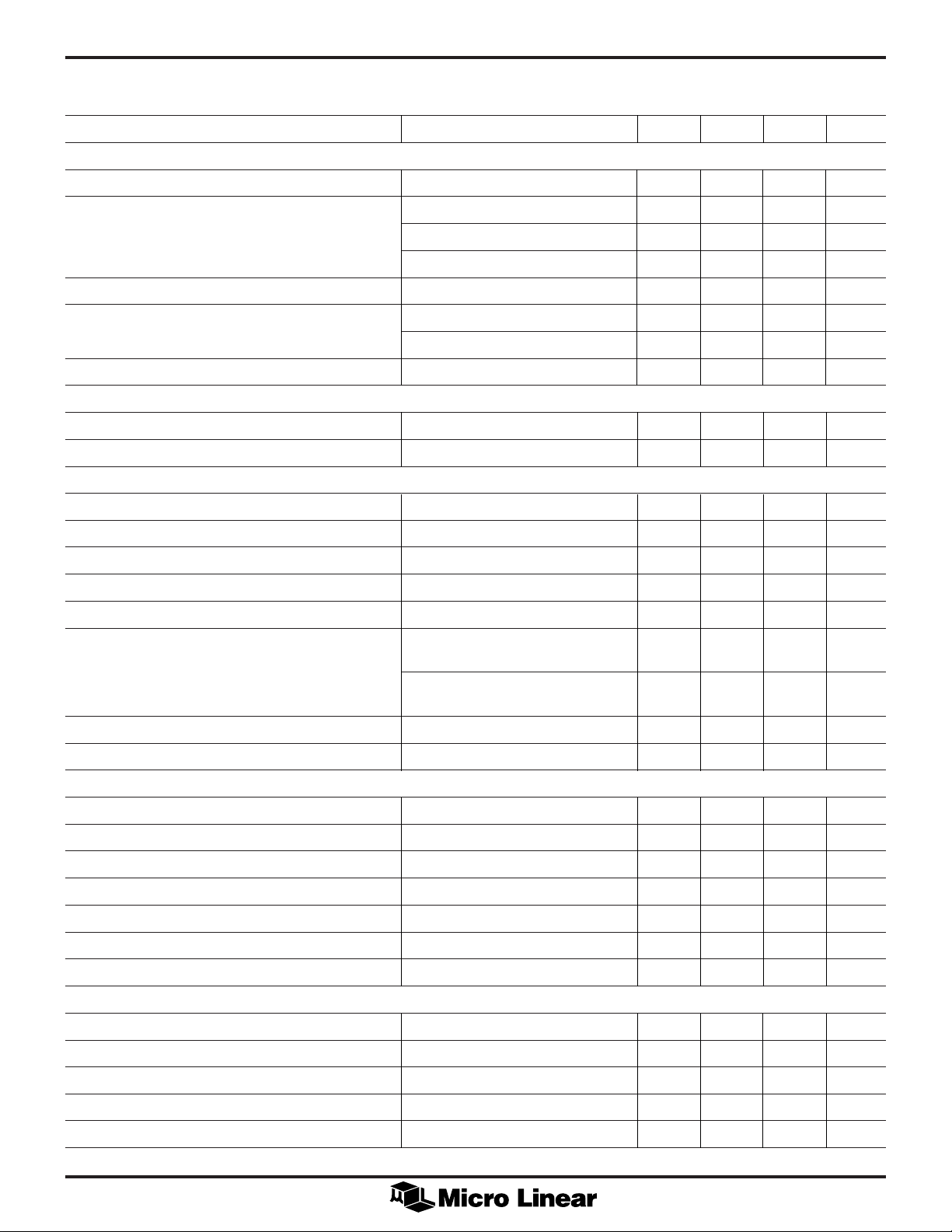
ELECTRICAL CHARACTERISTICS (Continued)
PARAMETER CONDITIONS MIN TYP MAX UNITS
GAIN MODULATOR
Output Voltage (V
Output Voltage Limit I
Offset Voltage I
I
Input Voltage I
SINE
)I
MUL
= 100µA, V
SINE
I
= 300µA, V
SINE
I
=100µA, V
SINE
I
= 300µA, V
SINE
= 1.5mA, V
SINE
= 0µA, V
SINE
I
= 150µA, V
SINE
= 200µA 0.8 1.4 1.8 V
SINE
EA–/OVP
= 3V 85 mV
EA OUT
= 3V 260 mV
EA OUT
= 6V 200 mV
EA OUT
= 6V 600 mV
EA OUT
= 0V 0.9 1 1.1 V
EA–/OVP
= 0V 15 mV
= 3V 15 mV
EA–/OVP
PFC CURRENT — LIMIT COMPARATOR
Current-Limit Threshold –0.85 –1.0 –1.15 V
Propagation Delay 100mV step and 100mV overdrive 100 ns
OSCILLATOR
Initial Accuracy TA = 25°C 72 76 80 kHz
Voltage Stability V
– 4.0V < VCC < V
CCZ
– 0.5V 1 %
CCZ
Temperature Stability 2%
Total Variation Line, temperature 69 83 kHz
Ramp Valley to Peak 2.5 V
C
Charging Current V
T
V
V
= 3V, V
LAMP FB
= 0.9V (Preheat) –90 –113 –130 µA
RX/CX
= 3V, V
LAMP FB
RT/CT
RT/CT
= 2.5V,
= 2.5V,
RX/CX = Open –180 –230 –260 µA
CT Discharge Current V
= 2.5V 4.0 5.5 7.0 mA
RT/CT
Output Drive Deadtime 0.64 0.91 1.30 µs
REFERENCE SECTION
Output Voltage TA = 25°C, IO = 1mA 7.4 7.5 7.6 V
Line regulation V
– 4.0V < VCC < V
CCZ
– 0.5V 8 25 mV
CCZ
Load regulation 1mA < IO < 5mA 2 15 mV
Temperature stability 0.4 %
Total Variation Line, load, temp 7.35 7.65 V
Output Noise Voltage 10Hz to 10kHz 50 µV
Long Term Stability TJ = 125°C, 1000 hrs 5 mV
PREHEAT AND INTERRUPT TIMER (RX = 680KW, CX = 4.7µF)
Initial Preheat Period 0.8 s
Subsequent Preheat Period 0.7 s
Start Period 1.2 s
Interrupt Period 5.7 s
Pin 10 Charging Current –24 –28 –33 µA
4
ML4832
ELECTRICAL CHARACTERISTICS (Continued)
PARAMETER CONDITIONS MIN TYP MAX UNITS
PREHEAT AND INTERRUPT TIMER (RX = 680KW, CX = 4.7µF) CONTINUIED
Pin 10 Open Circuit Voltage VCC < Start-up threshold 0.4 0.7 1.0 V
Pin 10 Maximum Voltage 7.0 7.3 7.7 V
Input Bias Current V
= 1.2V 0.1 µA
RX/CX
Preheat Lower Threshold 1.05 1.22 1.36 V
Preheat Upper Threshold 4.4 4.77 5.15 V
Interrupt Recovery Threshold 1.05 1.22 1.36 V
Start Period End Threshold 6.05 6.6 7.35 V
INTERRUPT INPUT
Interrupt Threshold 7.15 7.4 7.65 V
Input Bias Current 0.1 µA
R
Voltage 2.4 2.5 2.6 V
SET
OVP COMPARATOR
OVP Threshold 2.65 2.75 2.85 V
Hysteresis 0.20 0.25 0.27 V
Propagation Delay 1.4 µs
OUTPUTS
Output Voltage Low I
Output Voltage High I
Output Voltage Low in UVLO I
= 20mA 0.1 0.2 V
OUT
I
= 200mA 1.0 2.0 V
OUT
= –20mA V
OUT
I
= –200mA V
OUT
= 10mA, VCC 8V 0.2 V
OUT
– 0.2 VCC – 0.1 V
CC
– 2.0 VCC – 1.0 V
CC
Output Rise/Fall Time CL = 1000pF 20 ns
UNDER-VOLTAGE LOCKOUT AND BIAS CIRCUITS
IC Shunt Voltage (V
)I
CCZ
= 15mA 14.2 15.0 15.8 V
CC
Start-up Current VCC = Start-up threshold –0.2V 0.34 0.48 mA
Operating Current VCC = 12.5V, V
EA–/OVP
= V
V
= 0V, 5.5 8.0 mA
IA+
= 2.3V,
LAMP FB
IA OUT = open
RT = 16.2kW, R
= 22.1kW
SET
VCC = 12.5V, CL = 0
Start-up Threshold V
Shutdown Threshold V
– 1.2 V
CC
– 5.5 V
CC
– 1.0 VCC – 0.8 V
CCZ
– 5.0 VCC – 4.5 V
CCZ
Shutdown Temperature (TJ) 120 °C
Hysteresis (TJ) 30 °C
Note 1: Limits are guaranteed by 100% testing, sampling or correlation with worst case test conditions.
5
 Loading...