

Micro Linear Corporation ML4828IS, ML4828CP, ML4828CS, ML4828IP Datasheet
May 1997
ML4828*
BiCMOS Phase Modulation/Soft Switching Controller
GENERAL DESCRIPTION
The ML4828 is a complete BiCMOS phase modulation
control IC suitable for full bridge soft switching converters.
Unlike conventional PWM circuits, the phase modulation
technique allows for zero voltage switching (ZVS)
transitions and square wave drive across the transformer.
The IC modulates the phases of the two sides of the bridge
to control output power.
The ML4828 can be operated in either voltage or current
mode. Both cycle-by-cycle current limit, integrating fault
detection, and soft start reset are provided. The undervoltage lockout circuit features a 1.5V hysteresis with a
low starting current to allow off-line start up with a bleed
FEATURES
■ 5V BiCMOS for low power and high frequency
(1MHz) operation
■ Full bridge phase modulation zero voltage switching
circuit with independent programmable delay times
■ Current or voltage mode operation capability
■ Cycle-by-cycle current limiting with integrating fault
detection and restart delay
■ Can be externally synchronized
■ Four 3Ω CMOS output drivers
■ Under-voltage lockout circuit with 1.5V hysteresis
resistor. A shutdown function powers down the IC, putting
it into a low quiescent state.
The circuit can be operated at frequencies up to 1MHz.
The ML4828 contains four high current CMOS outputs
which feature high slew rate with low cross conduction. *Some Packages Are End Of Life
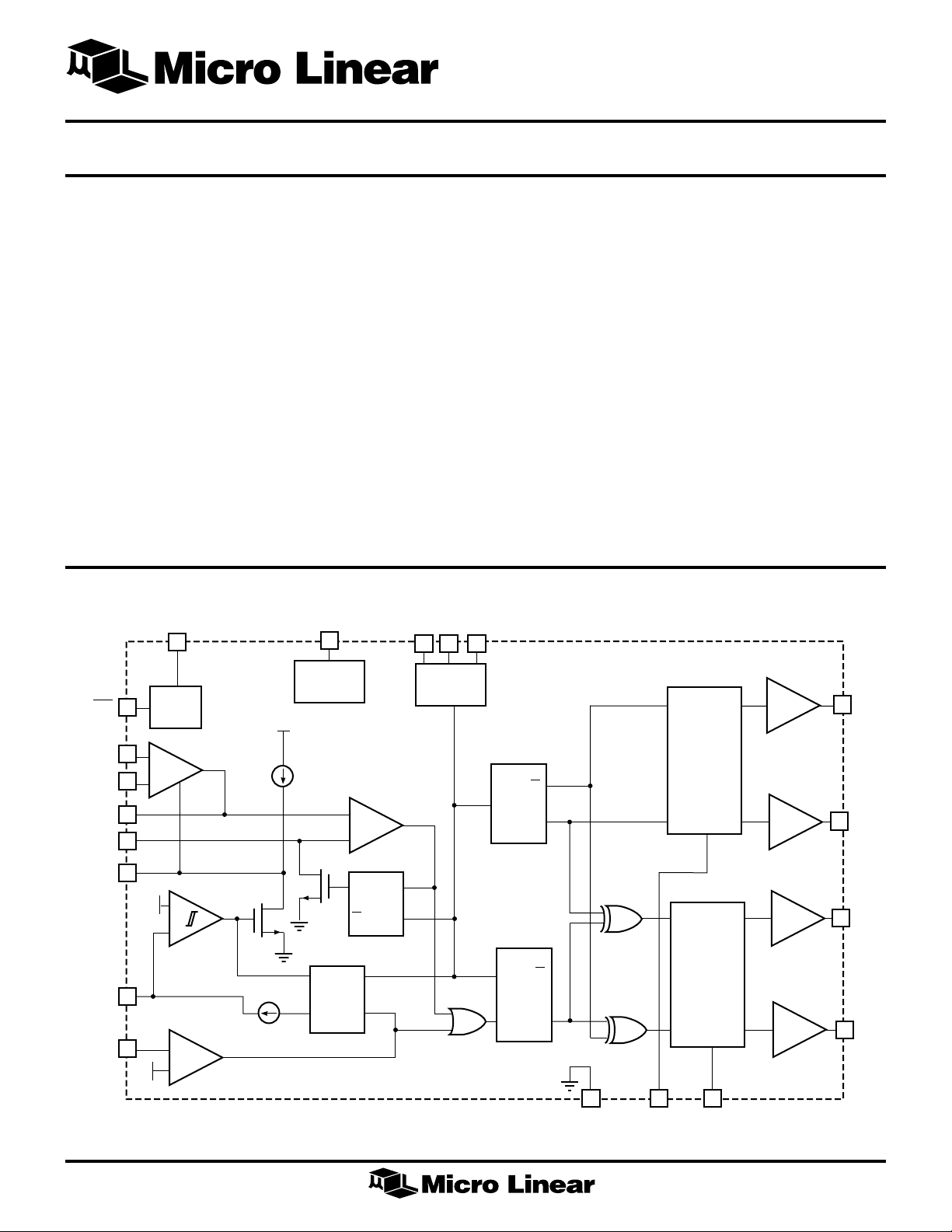
BLOCK DIAGRAM
V
V
CC
14
REF
5
SYNC RTC
643
T
2.5V REF
SDN DRIVER
EA+
EA–
EAO
RAMP
SS
RST
I
LIM
19
10
9
8
11
7
1.25V
12
20
2.5V
1V
+
–
UVLO
+
–
+
–
ERROR
AMP
I
LIM
IRST
ISS
FAULT
LOGIC
–
+
Q
Q
ΦMOD
S
R
OSC
DELAY A
Q
T
Q
Q
R
Q
S
GND
DELAY B
1
R
A
217
R
B
DRIVER
DRIVER
DRIVER
A1
18
A2
16
B1
15
13
B2
1
ML4828
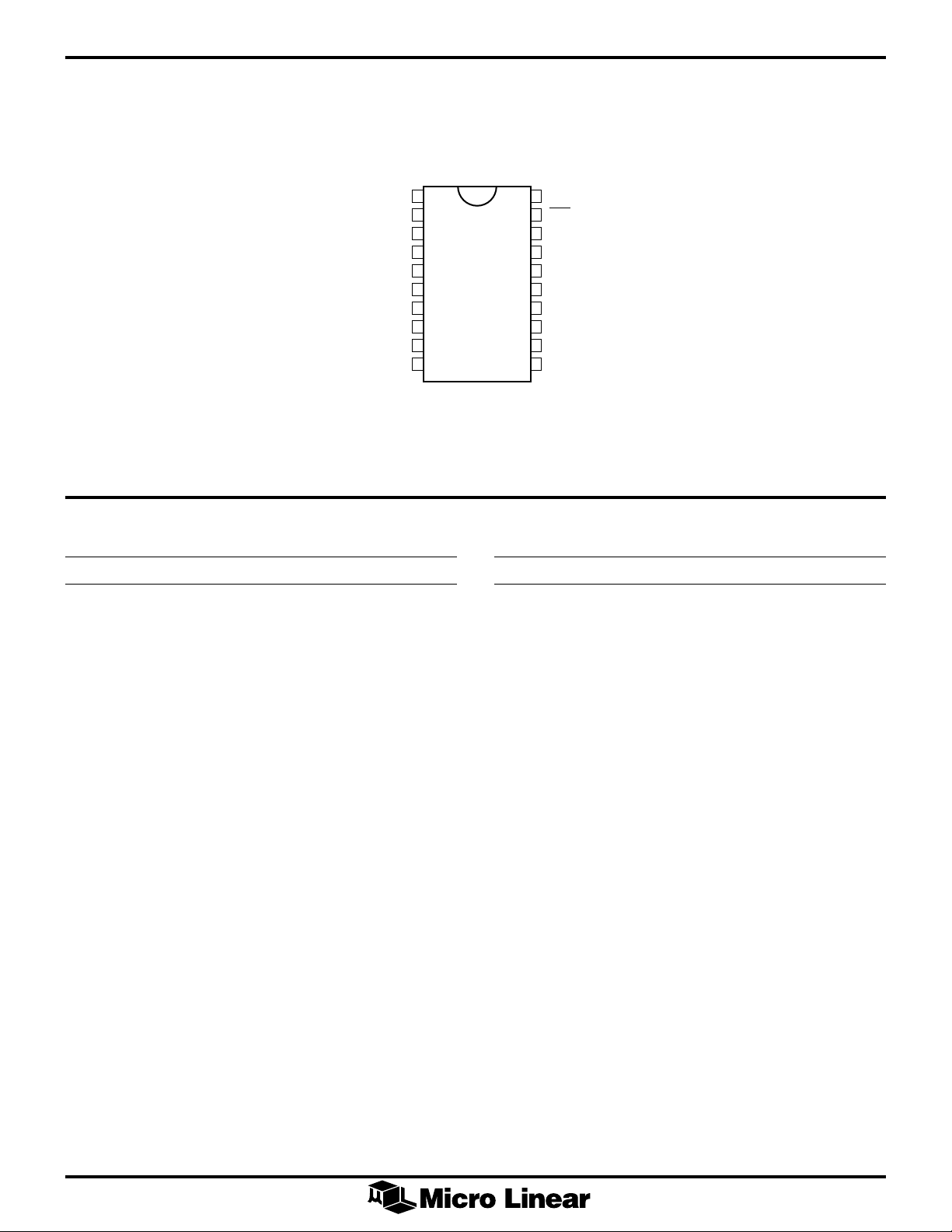
PIN CONNECTION
ML4828
20-Pin DIP (P20)
20-Pin SOIC (S20)
1
RA
2
R
B
3
R
T
4
C
T
5
REF
EA0
EA–
EA+
6
7
SS
8
9
10
TOP VIEW
SYNC
I
LIM
SDN
A1
GND
A2
B1
V
CC
B2
RST
RAMP
20
19
18
17
16
15
14
13
12
11
PIN DESCRIPTION
PIN NAME DESCRIPTION
1R
A
2R
B
3R
T
4C
T
5 REF 2.5V reference voltage.
6 SYNC Synchronization input to oscillator.
7 SS Soft start capacitor connection.
8 EAO Error amplifier output.
9 EA- Error amplifier inverting input.
10 EA+ Error amplifier non-inverting input.
A1 and A2 delay programming
resistor.
B1 and B2 delay programming
resistor .
Oscillator charge current
programming resistor.
Oscillator timing capacitor.
PIN NAME DESCRIPTION
11 RAMP RC network for phase modulator
ramp input.
12 RST RC network for reset and integrating
fault detect.
13 B2 B2 driver output.
14 V
CC
Power supply
15 B1 B1 driver output.
16 A2 A2 driver output.
17 GND Ground.
18 A1 A1 driver output.
19 SHDN Active low device shutdown.
20 I
LIMIT
Current limit control input
2
ML4828
ABSOLUTE MAXIMUM RATINGS
Soft Start Discharge Current ...................................... 5mA
CT Charging Current................................................. –1mA
Absolute maximum ratings are those values beyond which
the device could be permanently damaged. Absolute
maximum ratings are stress ratings only and functional
device operation is not implied.
V
.................................................................................................. 7V
CC
Output Current, Source or Sink (A1, A2, B1, B2)
Junction Temperature .............................................. 150°C
Storage Temperature Range ...................... –65°C to 150°C
Lead Temperature (Soldering 10 sec.) ...................... 260°C
Thermal Resistance (θ
)
JA
Plastic DIP ........................................................ 67°C/W
Plastic SOIC ..................................................... 95°C/W
Pulse (0.5 µs) ......................................................... 1.0A
Analog Inputs (EA+, EA–, EAO,
RST, RAMP, RST)............................ –0.3V to VCC + 0.3V
RT Source Current .................................................... –1mA
Error Amplifier Output Current ................................ ±2mA
OPERATING CONDITIONS
Temperature Range
ML4828CX ................................................. 0°C to 70°C
ML4828IX ............................................... –40°C to 85°C
ELECTRICAL CHARACTERISTICS
Unless otherwise specified, RA = R
(Notes 1,2)
PARAMETER CONDITIONS MIN TYP. MAX UNITS
OSCILLATOR
Initial Accuracy TA = 25°C 340 360 380 kHz
Voltage Stability 4.5V < VCC < 5.5V 4 5.3 %/V
Temperature Stability 2%
= 33.3kΩ, RT = 16kΩ, C
B
= 270PF, V
T
= 5V, TA = Operation Temperature Range
CC
Total Variation Line, temp. 325 400 kHz
CT Discharge Current VCT = 2V 1.15 1.5 mA
Ramp Peak 2.6 V
Ramp Valley 1.12 V
REFERENCE
Initial Accuracy TA = 25°C, IO = 250µA 2.475 2.5 2.525 V
Line Regulation 4.5V < VCC < 6.5V ±0.2 ±1 %/V
Load Regulation 100µA to 1mA ±0.5 ±6mV
Temperature Stability 0.45 %
Total Variation Line, Load, & Temp 2.44 2.54 V
Long Term Stability TJ = 125°C, 1000 hrs 5 25 mV
Short Circuit Current V
ERROR AMPLIFIER
Input Offset Voltage –20 20 mV
Input Common-Mode Range 0 1.75 V
Open Loop Gain 1V < VO < 2.7V 60 80 dB
PSRR 4.5V < V
Output Sink Current VO = 0.5V 1.2 1.9 mA
= 0V –10 –23 –35 mA
REF
< 6.5V 60 80 dB
CC
Output Source Current VO= 2.7V –0.35 –1.1 mA
Output High Voltage I
Output Low Voltage I
Unity Gain Bandwidth 7 10 MHz
Slew Rate 510 V/µs
= –500µA 2.6 2.85 V
SOURCE
= 500µA 0.1 0.2 V
SINK
3
ML4828
ELECTRICAL CHARACTERISTICS (Continued)
PARAMETER CONDITIONS MIN TYP. MAX UNITS
PHASE MODULATOR
EAO Zero Duty Cycle Threshold VRT = 0V 0 0.5 0.9 V
RAMP Delay to Output 50 80 ns
RAMP Discharge Current 48 95 mA
SOFT-START
Charge Current VSS = 4V –25 –50 µA
Discharge Current VSS = 1V 6 10 13.2 mA
CURRENT LIMIT/SHUTDOWN
Current Limit Threshold 0.9 1.0 1.1 V
Pin 20 Delay to Output (Note 1) 50 ns
Pin 12 Shutdown Threshold 1.0 1.1 1.5 V
Pin 12 Restart Threshold 2.2 2.4 2.6 V
Pin 12 Charging Current –350 –460 –550 µA
SDN Shutdown Threshold 1.05 1.6 2.05 V
OUTPUT
Output Low Level I
Output High Level I
= 20 mA 0.01 0.1 V
OUT
I
= 100 mA 0.1 0.3 V
OUT
= –20 mA 4.9 4.95 V
OUT
I
= –100 mA 4.6 4.7 V
OUT
Rise/Fall Time CL = 1000pF, (Note 1) 5 7 ns
ZVS Programmable Delay 240 280 315 ns
Delay Mismatch 0ns
R
/RB Reference Voltage 2.45 2.5 2.55 V
A
UNDER VOLTAGE LOCKOUT
Start Threshold 5.1 5.85 6.6 V
Stop Threshold 4.1 4.2 4.3 V
SUPPLY
Start Up Current V
6V 0.6 1 mA
CC <
Shutdown Current 100 500 µA
I
CC
Note 1: Limits are guaranteed by 100% testing, sampling, or correlation with worst-case test conditions.
Note 2: V
must be brought above the UVLO start voltage (6V) before dropping to VCC = 5V to ensure start-up.
CC
V
= 5V, CL = 1000pF, TA = 25°C57mA
CC
4
 Loading...