

Micro Linear Corporation ML4669CQ, ML4664CQ, ML4664IQ, ML4669IQ, ML4669CH Datasheet
...
July 2000
ML4664*/ML4669*
10BASE-FL to 10BASE-T Converter
GENERAL DESCRIPTION
The fully pin-compatible ML4664/ML4669 pair provide
FEATURES
■ Full duplex operation
conversion from 10BASE-T copper media to 10BASE-FL
fiber media in a single chip. They are compliant with
■ Five network status LED outputs
Ethernet IEEE 802.3 10BASE-T and 10BASE-FL standards.
The ML4664/69 uses a single 5V supply, and requires no
■ Industrial temperature option
crystal or clock.
10BASE-FL FEATURES:
Their 10BASE-FL transmitter offers a current drive output
that directly drives a fiber optic LED transmitter. Their
receiver offers a highly stable fiber optic data quantizer
capable of accepting input signals as low as 2mV
P-P
with
a 55dB dynamic range.
The 10BASE-T portion of the pair contains current driven
transmitter outputs that offer superior performance
■ Highly stable data quantizer with 55dB input dynamic
range
■ Input sensitivity as low as 2mV
■ Up to 100mA maximum current driven fiber optic LED
output for accurate launch power (PLCC package)
because their switching is highly symmetric, resulting in
lowered RFI noise and jitter. By changing one external
10BASE-T FEATURES:
resistor the pair easily interfaces to 100W unshielded
twisted pair, 150W shielded twisted pair, or a range of
■ Current driven output for low RFI noise and low jitter
other characteristic impedances.
■ Drives 100W unshielded or 150W shielded twisted pair
The ML4664 does not pass along disconnect information,
while the ML4669 does. A loss of light at the optical
■ Polarity detect status pin capable of driving an LED
inputs does not stop link pulses from being sent at the
twisted pair transmitter in the ML4664, but in the
■ Automatic polarity correction
ML4669 the link pulses stop. Also, a loss of link at the
twisted pair inputs will not stop the optical transmitter
■ On-chip link test with enable/disable option
from sending idle in the ML4664, but the ML4669 stops
sending idle. * Some Packages Are Obsolete
P-P
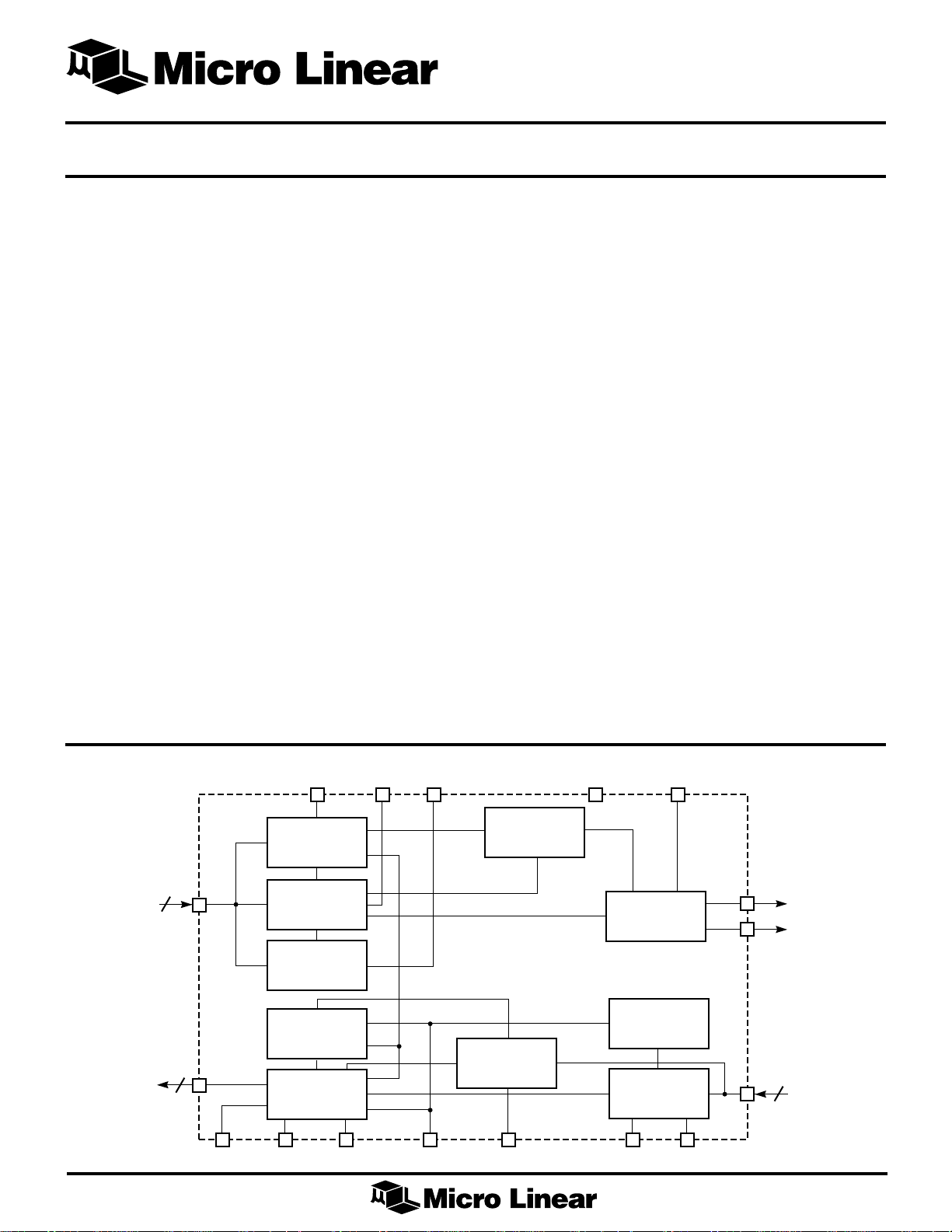
BLOCK DIAGRAM
TPIN
2
TPOUT
2
RTSETTP TxCAP0 TxCAP1
LINK PULSE
CHECK
RX SQUELCH
TP
POLARITY
CORRECT
LINK PULSE
GENERATOR
TP
TX
TPLED
RX SQUELCH
LMON
(LOW LIGHT)
IDLE
GENERATOR
TP
OPLED
OP
TX
THRESHOLD
GENERATOR
QUANTIZER
V
DC
RTSETOPRRSETPOLDISLTF
C
TIMER
OPOUT
OPVCC
2
OPIN
1
ML4664/ML4669
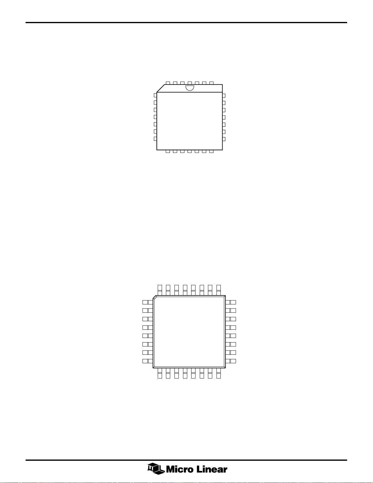
PIN CONFIGURATION
ML4664/ML4669
28-Pin PLCC (Q28)
TPINN
V
CC
TxCAP0
TxCAP1
GND
TPOUTN
TPOUTP
TPLED
LTF
CC
V
RTSETP
C
RRSET
TIMER
TPINP
4 3 2 1 28 27 26
5
6
7
8
9
10
11
12 13 14 15 16 17 18
POLDIS
TOP VIEW
OPLED
AVCCOPINP
LMON
RTSETOP
25
24
23
22
21
20
19
OPVCC
OPINN
AGND
V
THADJ
V
REF
V
DC
GND
OPOUT
TPINN
NC
V
CC
TxCAP0
TxCAP1
GND
TPOUTN
TPOUTP
ML4664/ML4669
32-Pin TQFP (H32-7)
TPLED
LTF
RTSETP
POLDIS
TOP VIEW
TIMER
C
OPLEDNCAVCCOPINP
CC
V
RRSET
RTSETOP
LMON
TPINP
32 31 30 29 28 27 26 25
1
2
3
4
5
6
7
8
9 10111213141516
NC
24
23
22
21
20
19
18
17
OPVCC
OPINN
AGND
V
THADJ
V
REF
V
DC
NC
GND
OPOUT
2

ML4664/ML4669
PIN DESCRIPTION
PIN NAME FUNCTION
1(29) C
2(30) LTF Link Test Fail. Active high. Normally
3(31) TPLED Indicates that reception is taking place
4(32) TPINP Twisted Pair receive data input.
5(1) TPINN When this signal exceeds the
TIMER
A capacitor from this pin to V
determines the Link Monitor response
time.
this pin is low, indicating that the link
is operational. If the link goes down
resulting from the absence of link
pulses or frames being received, the
chip will go into the Link Test Fail
state and bring LTF high.
When the ML4664 is in the link test
fail state, the optical and twisted pair
transmitters are disabled from sending
data. However, the optical transmitter
does send an idle signal, and link
pulses are sent at the twisted pair
transmitter. When the ML4669 is in
link test fail state, the optical and
twisted pair transmitters are disabled
from sending data. Also, the optical
transmitter will not send an idle
signal. However, link pulses may be
sent at the twisted pair transmitter,
depending on the optical inputs. See
Table 1.
This pin may be grounded to disable
Link Test. In this mode no link pulses
are sent and the link will not fail if no
link pulses are received. If this pin is
not used as an LED driver, and is not
grounded, a 2kW 5% resistor should
be connected between this pin and
VCC.
on the TPINP, TPINN pair. Active low
LED driver, open collector. It is
extended 16ms for visibility.
Optionally, this pin may be grounded
to disable the optical output. If this
pin is not used as an LED driver and is
not grounded, a 2kW, 5% resistor
should be connected between TPLED
and VCC.
receive squelch requirements the
receive data is buffered and sent
to the Rx± outputs.
(Pin Number in Parentheses is for TQFP Version)
CC
PIN NAME FUNCTION
7(4) TxCAP0 An external capacitor of 680pF is
8(5) TxCAP1 tied between these two pins to set
the pulse width for the preequalization on the twisted pair
transmitter. If these two pins are
shorted together, no pre- equalization
occurs. If the ML4664/ML4669 is
driving only a short cable, or board
traces, these pins may be shorted.
9(6) GND Ground reference
20(18)
10(7) TPOUTN Pre-equalized differential balanced
11(8) TPOUTP current driven output. These outputs
are connected to a balanced transmit
output filter which drives the twisted
pair cable through pulse transformers.
The output current is set with an
external resistor connected to RTSET
allowing the chip to drive 100W
unshielded , 150W shielded twisted
pair cables or a range of other
characteristic impedances.
12(10) POLDIS Receive Polarity status. Active low
LED Driver, open collector output.
Indicates the polarity of the receive
twisted pair regardless of auto polarity
correction. When low, receive polarity
is reversed. When high, receive
polarity is correct. This pin may be
grounded to disable the polarity
circuit. If this pin is not used as an
LED driver, and is not grounded, a
2kW, 5% resistor should be connected
between this pin and VCC.
13(11) RTSETTP When using 100W unshielded twisted
pair, a 220W resistor is tied between
this pin and VCC. When using 150W
shielded twisted pair, a 330W resistor
is tied between this pin and VCC.
15(13) RRSET A 1% 61.9kW resistor tied from this
pin to VCC is used for internal biasing.
16(14) RTSETOP Sets the current driven output of the
transmitter. A 115W resistor should be
tied between this pin and VCC.
6(3) V
14(12)
CC
5V input
3

ML4664/ML4669
PIN DESCRIPTION
PIN NAME FUNCTION
17(15) LMON Link Monitor “Low Light” LED status
output. Pulled low when voltage on
the OPINP, OPINN inputs exceed min
threshold set by V
transitions on OPINP, OPINN
indicating an idle signal or active
data. If the voltage on OPINP, OPINN
inputs falls below the minimum
threshold or transitions cease on
OPINP, OPINN, LMON will go high.
Active low LED driver, open collector.
In the low light state, optical and
twisted pair transmitters are disabled
from sending data. The optical
transmitter of the ML4664 does send
an idle signal, and link pulses are sent
at the twisted pair transmitter. For the
ML4669, the twisted pair transmitter
will not send link pulses, the optical
transmitter may send an idle signal,
depending on inputs. See Table 1.
18(16) OPVCC 5V supply for fiber optic
LED driver
19(17) OPOUT Fiber optic LED driver output
(Continued)
THADJ
, and there are
PIN NAME FUNCTION
22(21) V
23(22) V
24(23) AGND Analog Filtered Ground
25(24) OPINN This input pin should be capacitively
26(25) OPINP This input pin should be capacitively
27(26) AV
28(28) OPLED Indicates reception is taking place on
REF
THADJ
CC
A 2.5V reference with respect to GND
This input pin sets the link monitor
threshold
coupled to filtered AVCC. The input
resistance is approximately 1.3kW.
coupled to the input source. The input
resistance is approximately 1.3kW.
Analog Filtered 5V
the OPINP, OPINN pair. Active low
LED driver, open collector. It is
extended 16ms for usability. This pin
may be grounded to disable the
twisted pair outputs. If this pin is not
used as an LED driver, and is not
grounded, a 2kW, 5% resistor should
be connected between this pin and
VCC.
21(20) V
DC
An external capacitor on this pin
integrates an error signal which nulls
the offset of the input amplifier. If the
DC feedback loop is not being used,
this pin should be connected to V
REF
.
4

ABSOLUTE MAXIMUM RATINGS
ML4664/ML4669
Absolute maximum ratings are those values beyond
which the device could be permanently damaged.
Absolute maximum ratings are stress ratings only and
Thermal Resistance (qJA)
PLCC ............................................................... 68°C/W
TQFP ............................................................... 80ºC/W
functional device operation is not implied.
OPERATING CONDITIONS
Power Supply Voltage Range
V
...................................................................GND –0.3 to 6V
CC
Input Voltage Range: Digital Inputs
(SQEN, LBDIS) ....................... GND –0.3 to VCC +0.3V
Tx+, Tx–, VIN+, VIN– .............. GND –0.3 to VCC +0.3V
Junction Temperature............................................. 150°C
Storage Temperature................................–65°C to 150°C
Lead Temperature (Soldering) ................................ 260°C
Temperature Range
ML4664/ML4669CX.................................. 0°C to 70°C
ML4664/ML4669IQ ...............................–40°C to 85°C
Supply Voltage (VCC) ......................................... 5V ± 5%
LED on Current ...................................................... 10mA
RRSET ........................................................ 61.9kW ± 1%
RTSETOP....................................................... 115W ± 1%
RTSETTP........................................................ 220W ± 1%
ELECTRICAL CHARACTERISTICS
Unless otherwise specified, TA = Operating Temperature Range, VCC = OPVCC = AVCC = 5V ± 5% (Note 1)
SYMBOL PARAMETER CONDITIONS MIN TYP MAX UNITS
I
CC
V
Power Supply Current RTSETOP = 115W 140 mA
While Transmitting
Reference Voltage C Suffix 2.30 2.60 V
REF
I Suffix 2.25 2.67 V
V
OL
I
OPOUT
I
TPOUT
V
TPSQ
H
TP
V
TPIN
R
TPIN
V
OPTH
H
OP
V
OPIN
R
OPIN
V
OPCM
A
V
V
OFF
V
N
I
TH
LED Drivers: V
OP Transmit Peak Output Current RTSETOP = 115 (Note 2) C Suffix 47 52 57 mA
TP Transmit Peak Output Current RTSETTP = 220 42 mA
TP Receive Squelch Voltage 300 450 585 mV
TP Receive Squelch Hysteresis 50 %
TP Receive Input Voltage 300 3100 mV
TP Receive Input Resistance 4 kW
OP Receive Input Threshold V
Voltage
OP Receive Input Threshold 20 %
Hysteresis
OP Receive Input Voltage 2 1600 mV
OP Receive Input Resistance 0.8 1.3 2.0 kW
OP Receive Common Mode 1.65 V
Voltage
Amplifier Gain 100 V/V
Input Offset VDC = V
Input Referred Noise 50MHz Bandwidth 25 µV
Input Bias Current at V
OL
THADJ
RL = 300 for OPLED, TPLED, 1.5 3.5 V
POLLED LTF, and LMON
I Suffix 46 58.5 mA
THADJ
V
THADJ
= V
REF
(DC Loop Inactive) 3 mV
REF
= V
REF
567mV
–200 0 200 µA
P-P
P-P
P-P
P-P
5
 Loading...