

Micro Linear Corporation ML4642CQ, ML4642CR Datasheet
April 1997
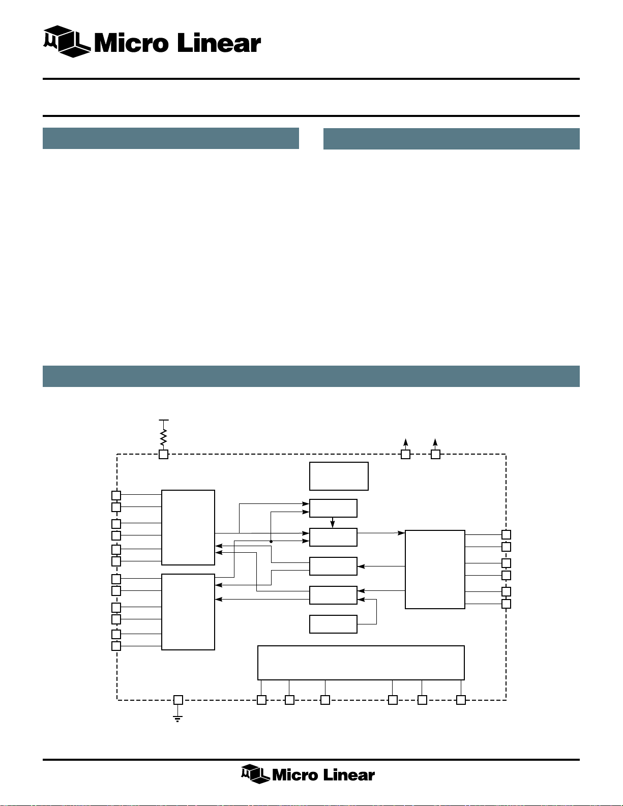
ML4642 AUI Multiplexer
GENERAL DESCRIPTION
The ML4642 AUI Multiplexer contains all the necessary
drivers/receivers and control logic to implement a 2 port
MAU when used in conjuction with a transceiver chip
which has a standard 802.3 AUI interface. In addition, the
ML4642 is capable of operating in stand-alone mode
where it interconnects two DTEs in the absence of a
network MAU. Several ML4642s can be cascaded
together to implement a 4 or 8 port MAU or stand-alone
device.
Logic within the ML4642 detects collisions resulting from
multiple DTEs transmitting simultaneously. In addition,
collision signals received from a transceiver attached at
the MAU port are propagated to both of the DTE ports.
Jabbering DTEs are prevented from loading down the
network by internal jabber timers which disable babbling
ports.
BLOCK DIAGRAM
+5V
FEATURES
■ IEEE 802.3 compliant AUI interfaces assure
compatibility with any AUI ready devices
■ No crystal or clock input
■ On-chip Jabber logic, Collision Detection, and SQE
test with enable/disable option
■ Selectable Loopback, Jabber, and SQE Test allows
cascading of multiple chips to increase DTE port
TXIN1P
TXIN1N
RXOUT1P
RXOUT1N
CDOUT1P
CDOUT1N
TXIN2P
TXIN2N
RXOUT2P
RXOUT2N
CDOUT2P
CDOUT2N
RRSET
61.9K
MAU
AUI
INTERFACE
MAU
AUI
INTERFACE
GND
JAB1/JDIS JAB2
CONTROL
LOGIC
JABBER
DO MUX
DI MUX
CI MUX
SQE SOURCE
LED DRIVERS
CDLED RXLED/LPBK/SQE
V
CC
V
DTE
AUI
INTERFACE
TXLED1
CC
TXOUTP
TXOUTN
RXINP
RXINN
CDINP
CDINN
TXLED2
1
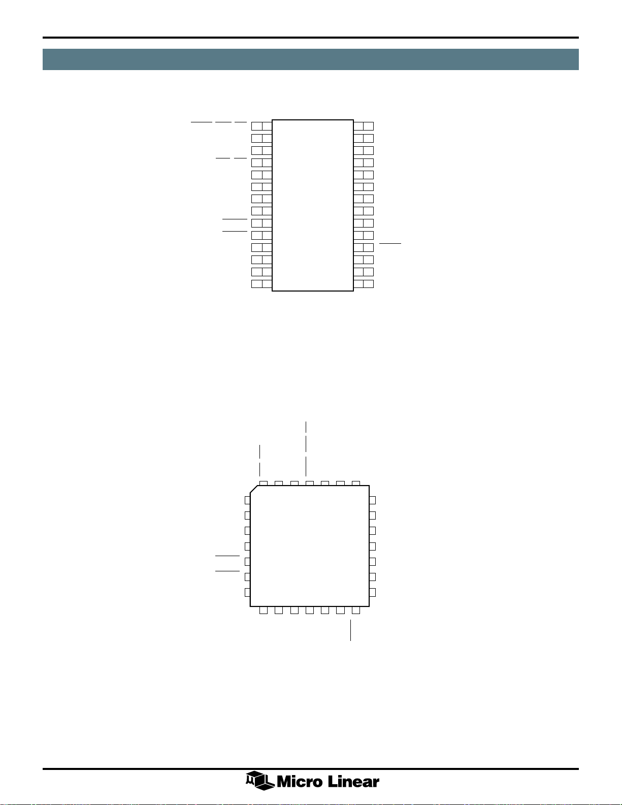
ML4642
PIN CONNECTIONS
ML4642
28-Pin SSOP (R28)
RXLED/LPBK/SQE
RXINP
RXINN
JAB1/JDIS
RRSET
V
TXOUTP
TXOUTN
TXLED1
TXLED2
TXIN2P
TXIN2N
TXIN1P
TXIN1N
1
2
3
4
5
CC
6
7
8
9
10
11
12
13
14
TOP VIEW
28-Pin PLCC (Q28)
ML4642
28
27
26
25
24
23
22
21
20
19
18
17
16
15
RXOUT1P
RXOUT1N
RXOUT2N
RXOUT2P
GND
CDOUT1N
CDOUT1P
JAB2
CDINP
CDINN
CDLED
CDOUT2P
CDOUT2N
V
CC
RRSET
V
CC
TXOUTP
TXOUTN
TXLED1
TXLED2
TXIN2P
JAB1/JDIS
RXINN
RXINP
RXLED/LPBK/SQE
432128
5
6
7
8
9
10
11
TOP VIEW
12 13 14 15 16
CC
V
TXIN1P
TXIN2N
TXIN1N
RXOUT1P
RXOUT1N
27 26
17 18
CDOUT2P
CDOUT2N
RXOUT2N
25
RXOUT2P
24
GND
23
CDOUT1N
22
CDOUT1P
21
JAB2
20
CDINP
19
CDINN
CDLED
2
ML4642
PIN DESCRIPTIONS
PIN NO. NAME FUNCTION DESCRIPTION
1 RXLED/LPBK/SQE I/O Active low receive LED driver for MAU port. If tied to ground, this pin
enables internal loopback of the active TXIN pair to the RXOUT pairs
and enables SQE test. If tied to 0.6 volts internal loopback is enable but
SQE test is disabled. SQE and loopback are disabled when this pin is
pulled high.
2 RXINP Input Receive signal pair for MAU port.
3 RXINN Onput Receive signal pair for MAU port.
4 JAB1/JDIS I/O Active low jabber LED driver for DTE port 1. If tied to ground, the
jabber function is disabled at TXIN1 and TXIN2.
5 RRSET Input Bias setting external resistor, 61.9Ký.
6V
7 TXOUTP Output Transmit signal pair for MAU port.
8 TXOUTN Output Transmit signal pair for MAU port.
9 TXLED1 Output Open collector, active low transmit LED driver for DTE AUI port 1.
10 TXLED2 Output Open collector, active low transmit LED driver for DTE AUI port 2.
11 TXIN2P Input Transmit signal pair for DTE port 2.
12 TXIN2N Input Transmit signal pair for DTE port 2.
13 TXIN1P Input Transmit signal pair for DTE port 1.
14 TXIN1N Input Transmit signal pair for DTE port 1.
15 V
16 CDOUT2N Output Collision signal pair for DTE port 2.
17 CDOUT2P Output Collision signal pair for DTE port 2.
18 CDLED Output Open collector, active low collision LED driver.
19 CDINN Input Collision signal pair for MAU port.
20 CDINP Input Collision signal pair for MAU port.
21 JAB2 Output Open collector, active low jabber LED driver for DTE port 2.
22 CDOUT1P Output Collision signal pair for DTE port 1.
23 CDOUT1N Output Collision signal pair for DTE port 1.
CC
CC
Power +5 volt power supply
Power +5 volt power supply
24 GND Ground GND.
25 RXOUT2P Output Receive signal pair for DTE port 2.
26 RXOUT2N Output Receive signal pair for DTE port 2.
27 RXOUT1N Output Receive signal pair for DTE port 1.
28 RXOUT1P Output Receive signal pair for DTE port 1.
3
ML4642
ABSOLUTE MAXIMUM RATINGS
Absolute maximum ratings are limits beyond which the
life of the integrated circuit may be impaired. All
voltages unless otherwise specified are measured with
OPERATING CONDITIONS
Supply Voltage (VCC) . . . . . . . . . . . . . . . . . . . 5V ± 10%
LED on Current. . . . . . . . . . . . . . . . . . . . . . . . . . . . 10mA
RRSET . . . . . . . . . . . . . . . . . . . . . . . . . . . . 61.9ký ± 1%
respect to ground.
Power Supply Voltage Range VCC. . . GND –0.3V to 6.0V
Input Current RRSET, JAB1/JABD, JAB2, CDLED,
RxLED/LPBK/SQE, TxLED1, TxLED2 . . . . . . . . . . 60mA
Junction Temperature . . . . . . . . . . . . . . . . . . . . . . 150°C
Storage Temperature . . . . . . . . . . . . . . . . –65°C to 150°C
Lead Temperature (Soldering 10 seconds) . . . . . . . 260°C
Thermal Resistance (qJA)
SSOP . . . . . . . . . . . . . . . . . . . . . . . . . . . . . . 109°C/W
PLCC . . . . . . . . . . . . . . . . . . . . . . . . . . . . . . . 68°C/W
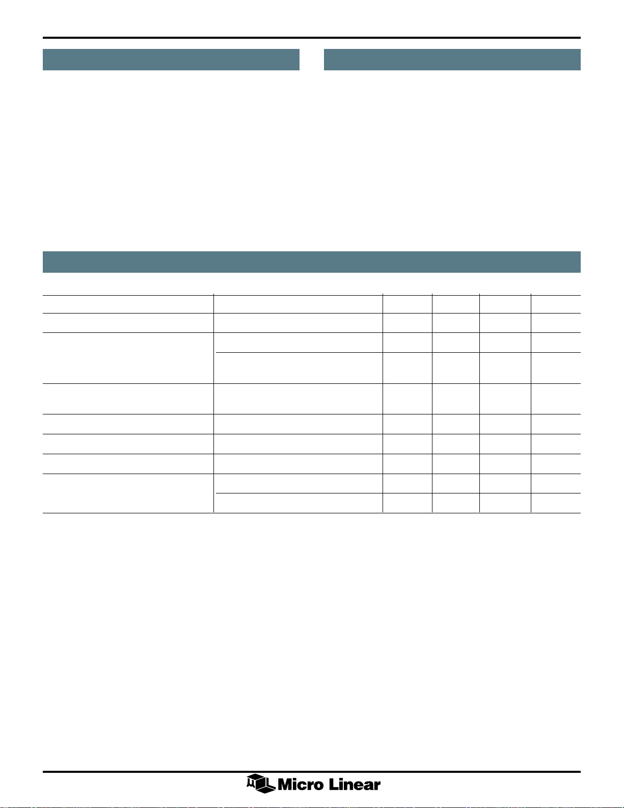
ELECTRICAL CHARACTERISTICS
Unless otherwise specified TA = 0°C to 70°C, VCC = 5V ± 10%. (Notes 1, 2)
PARAMETER CONDITIONS MIN TYP. MAX UNITS
Power Supply Current I
LED Drivers: V
OL
CC
V
= 5V, (Note 3) 60 120 mA
CC
RL=510ý for CDLED, TXLED1,2, JAB2 0.8 V
=270ý for JAB1/JDIS,
R
L
RxLED/LPBK/SQE 1.2 2.5 3.5 V
Transmit Squelch Voltage Level –300 –250 –200 mV
(Tx+, Tx–)
Differential Output Voltage ±550 ±1200 mV
Common Mode Output Voltage 4.0 V
Differential Output Voltage Imbalance 2 ±40 mV
RxLED/LPBK/SQE SQE Enabled/Loopback Enabled 0.3 V
SQE Disabled/Loopback Enabled 0.4 0.6 0.8 V
Note 1: Limits are guaranteed by 100% testing, sampling or correlation with worst case test conditions.
Note 2: Low Duty cycle pulse testing is performed at T
Note 3: This does not include the current from the AUI pull down resistors or the LED output pins.
.
A
4
ML4642
AC ELECTRICAL CHARACTERISTICS
SYMBOLS PARAMETER MIN TYP. MAX UNITS
TRANSMIT
t
TXNPW
t
TXFPW
t
XODY
t
TXLP
t
TXSDY
t
TXJ
Transmit Turn-On Pulse Width 20 ns
Transmit Turn-Off Pulse Width 180 ns
Transmitter Turn-On Delay 30 ns
Transmit Loopback Startup Delay 40 ns
Transmit Steady State Prop. Delay 15 ns
Transmitter Jitter 1 ns
RECEIVE
t
RXODY
t
RXSDY
t
RXJ
t
AR
Receive Turn-On Delay 20 ns
Receive Steady State Prop. Delay 15 ns
Receiver Jitter 1ns
Differential Output Rise Time 3 ns
20% to 80% (Rx+/–, COL+/–)
t
AF
Differential Output Fall Time 3 ns
20% to 80% (Rx+/–, COL+/–)
COLLISION
t
CPSQE
Collision Present to SQE Assert 0 200 ns
t
SQEXR
t
CLF
t
CLPDC
t
SQEDY
t
SQETD
t
SQEB
Time for SQE to Deactivate after a collision 100 900 ns
Collision Frequency 8.5 10 11.5 MHz
Collision Pulse Duty Cycle 40 50 60 %
SQE Test Delay (Tx Inactive to SQE) 0.6 1.1 1.6 µs
SQE Test Duration 0.5 1.0 1.5 µs
SQE Blank Period 4 7 µsec
JABBER, LINK TEST AND LED TIMING
t
JAD
t
JRT
t
JSQE
Jabber Activation Delay 7 13.5 20 ms
Jabber Reset Unjab Time 250 450 750 ms
Delay from Outputs Disabled to 100 ns
Collision Oscillator On
t
LEDT
CDLED, RxLED, TxLED1, TxLED2 On Time 20 50 300 ms
5
 Loading...