

Datasheet ML4624CQ, ML4622CP, ML4622CS, ML4622IS, ML4624CP Datasheet (Micro Linear Corporation)
January 1997
ML4622, ML4624
Fiber Optic Data Quantizer
GENERAL DESCRIPTION
The ML4622 and ML4624 data quantizers are low noise,
wideband, bipolar monolithic ICs designed specifically for
signal recovery applications in fiberoptic receiver systems.
They contain a wideband limiting amplifier which is
capable of accepting an input signal as low as 2mV
P-P
with a 55dB dynamic range. This high level of sensitivity
is achieved by using a DC restoration feedback loop
which nulls any offset voltage produced in the limiting
amplifier.
The output stage is a high speed comparator circuit with
both TTL and ECL outputs. An enable pin is included for
added control.
The Link Detect circuit provides a Link Monitor function
with a user selectable reference voltage. This circuit
monitors the peaks of the input signal and provides a
logic level output indicating when the input falls below
an acceptable level. This output can be used to disable
the quantizer and/or drive an LED, providing a visible link
status.
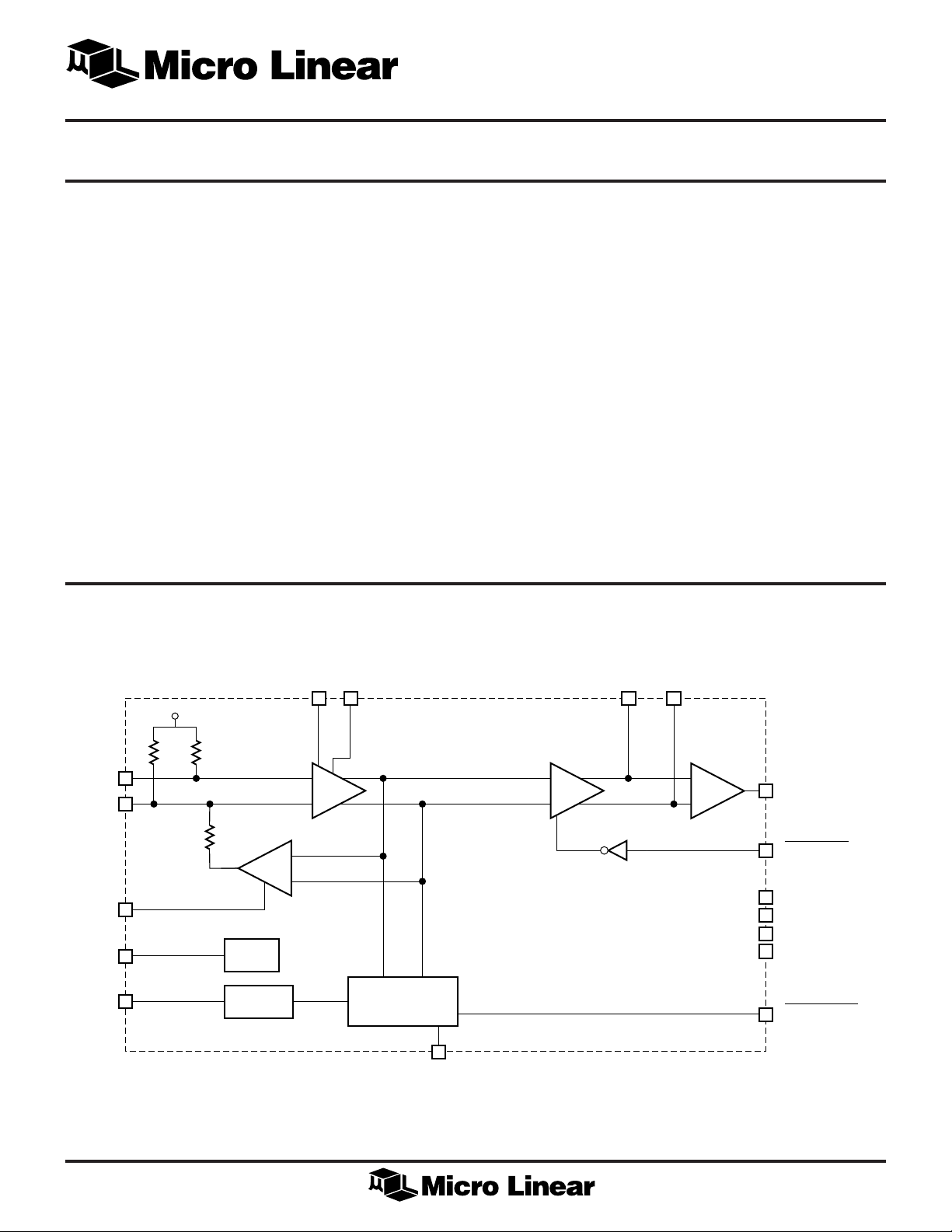
ML4622/ML4624 BLOCK DIAGRAM
FEATURES
■ Data rates up to 40MHz or 80MBd
■ Can be powered by either +5V providing TTL or raised
ECL level outputs or –5.2V providing ECL levels
■ Low noise design: 25µV RMS over bandwidth
■ Adjustable Link Monitor function with hystersis
■ Wide 55dB input dynamic range
■ Low power design
■ ML4624 is pin compatible with the ML4621
APPLICATIONS
■ IEEE 802.3 10BASE-FL Receiver
■ IEEE 802.5 fiber optic token ring, 4 and 16mbps
■ Fiber Optic Data Communications and
Telecommunications Receivers
V
IN
V
IN
V
DC
V
REF
VTHADJ
CF1
CF2
BIAS
+
AMP
–
ECL
CMP
ECL+
ECL–
TTL
CMP
TTL OUT
CMP ENABLE
∫
TTL*
V
CC
V
CC
GND
REF
THRESH
GEN
LINK DETECT
C
TIMER
*ML4624 ONLY
GND TTL
TTL LINK MON
1
ML4622, ML4624
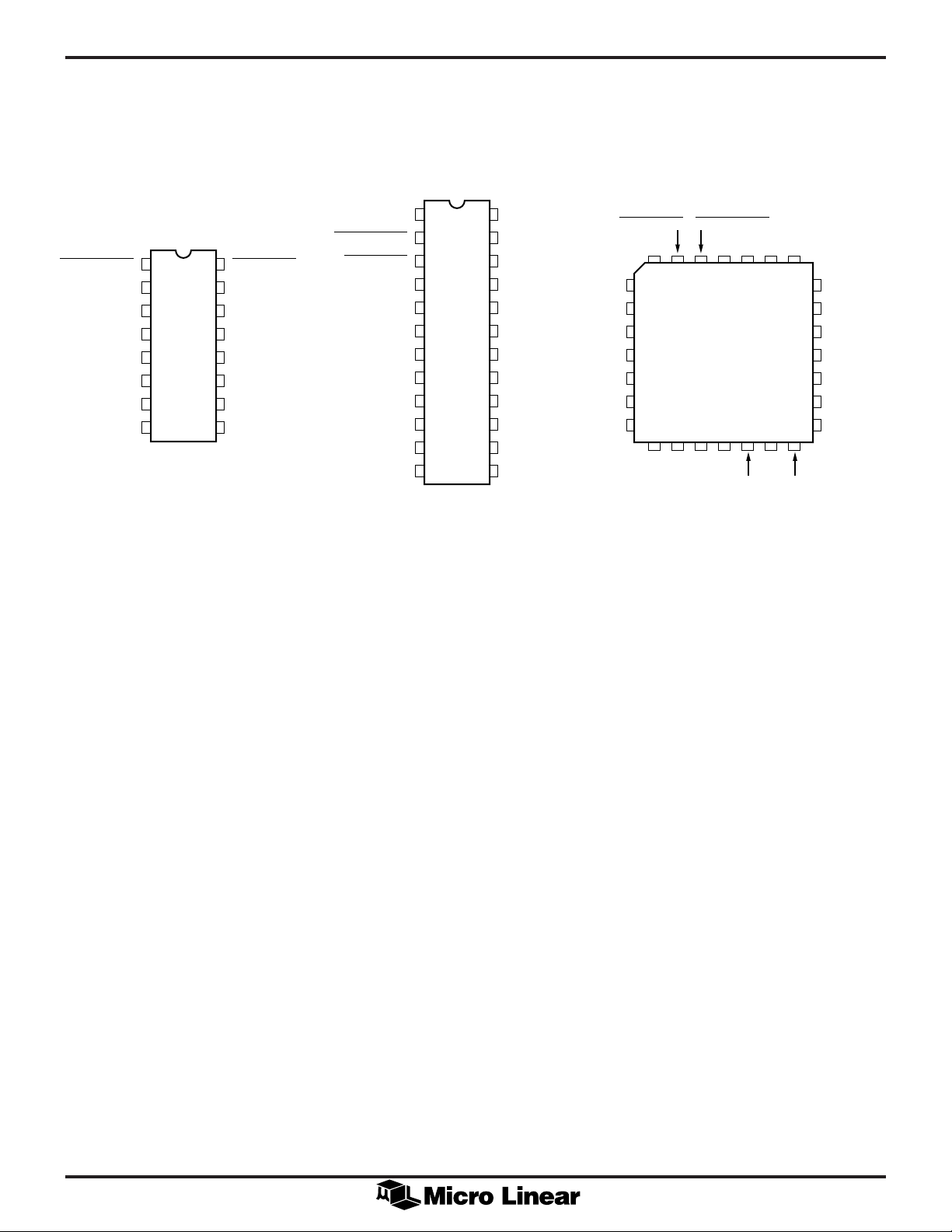
PIN CONNECTIONS
TTL LINK MON
GND
V
IN–
VIN+
V
DC
CF2
CF1
GND TTL
ML4622
16-Pin DIP or
SOIC (Narrow)
16
1
15
2
14
3
13
4
12
5
11
6
10
7
8
TOP VIEW
9
CMP ENABLE
ADJ
V
TH
V
REF
C
TIMER
V
CC
TTL OUT
ECL+
ECL–
24-Pin Narrow DIP
NC
TTL LINK MON
CMP ENABLE
V
IN
V
IN
V
DC
CF2
CF1
NC
NC
NC
NC
–
+
ML4624
1
2
3
4
5
6
7
8
9
10
11
12
TOP VIEW
24
23
22
21
20
19
18
17
16
15
14
13
V
CC
NC
NC
C
TIMER
V
REF
VTHADJ
GND
TTL OUT
TTL
V
CC
GND TTL
ECL+
ECL–
V
V
IN
V
CF2
CF1
ML4624
28-Pin PCC
4 3 2 1 28 27 26
5
–
IN
6
+
7
NC
8
DC
9
10
11
NC
12 13 14 15 16 17 18
NC NC NC NC ECL+
TTL LINK MONCMP ENABLE
NC V
NC NCNC
CC
25
24
23
22
21
20
19
ECL– GND TTL
NC
C
TIMER
V
REF
VTHADJ
GND
TTL OUT
TTL
V
CC
2

PIN DESCRIPTION
ML4622, ML4624
NAME FUNCTION
TTL LINK MON TTL Link Monitor output. Signal is
low when the VIN+, VIN– inputs
exceed the minimum threshold,
which is set by a voltage on the
VTHADJ pin. Signal is high when the
input signal level is below the
threshold. Capable of driving a 10mA
LED indicator. This pin can be tied to
CMP ENABLE.
CMP ENABLE A low voltage at this TTL input pin
enables both the ECL and the TTL
outputs. A high TTL voltage disables
the comparator output with ECL+
high, ECL– low, and TTL OUT high.
VIN– This input pin should be capacitively
coupled to the input source or to
filtered ground. (The input resistance
is approximately 1.6kΩ.)
VIN+ This input pin should be capacitively
coupled to the input source or to
filtered ground. (The input resistance
is approximately 1.6kΩ.)
ECL– The ECL comparator negative output.
Has internal pull down resistor.
External pull downs are not required
unless driving a large capacitive
load.
ECL+ The ECL comparator positive output.
Has internal pull down resistor.
External pull downs are not required
unless driving a large capacitive
load.
GND TTL The negative supply for the TTL
comparator stage. If the TTL output is
not necessary, connect GND TTL
to VCC.
NAME FUNCTION
VCC TTL The positive supply for the TTL
comparator stage. If the TTL output is
not necessary, connect VCC TTL to
VCC. (ML4624 only)
TTL OUT TTL data output.
V
DC
CF2 A capacitor from this pin to CF1
CF1 Connect to CF2 through a capacitor.
GND Negative supply. Connect to –5.2V
VTHADJ This input pin sets the link monitor
V
REF
C
TIMER
V
CC
An external capacitor on this pin
integrates an error signal which nulls
the offset of the input amplifier. If the
DC feedback loop is not being used,
this pin should be connected to V
controls the maximum bandwidth of
the amplifier.
for ECL operation, or to ground for
TTL or raised ECL operation.
threshold.
A 2.5V reference with respect to
GND.
A capacitor from this pin to V
determines the Link Monitor
response time.
Positive supply. Connect to ground
for negative ECL operation, or to 5V
for TTL or raised ECL operation.
CC
REF
.
3

ML4622, ML4624
ABSOLUTE MAXIMUM RATINGS
VCC – GND . . . . . . . . . . . . . . . . . . . . . . . . . . . . . . –0.3 to +7.0
V
TTL – GND TTL . . . . . . . . . . . . . . . . . . . . . . . –0.3 to +7.0
CC
Inputs/Outputs GND . . . . . . . . . . . . . . . . . . . –0.3 to V
Storage Temperature Range . . . . . . . . . . . . . . –65°C to +150°C
Lead Temperature (Soldering 10 sec.) . . . . . . . . . . . . . . +260°C
ML4622, ML4624 ELECTRICAL CHARACTERISTICS (Note 2 and 3)
Over recommended operating conditions of T
industrial temperature range, V
SYMBOL PARAMETER MIN TYP MAX UNITS CONDITIONS
= 5V ± 10%, GND = 0V unless otherwise noted (Note 1).
CC
A
+0.3
CC
= 0°C to 70°C for commercial temperature range, TA = –40°C to +85°C for
I
CC1
VCC Supply Current 35 45 mA GND TTL = V
(TTL Output Disabled)
I
CC2
VCC Supply Current 55 70 mA GND TTL = GND
(TTL Output Enabled)
V
I
VREF
A
V
REF
V
IN
Reference Voltage 2.40 2.50 2.60 V
V
Output Source Current 5 mA
REF
Amplifier Gain 100 V/V
Input Signal Range 2 1600 mV
P–P
VTHADJ External Voltage at VTHADJ 0.5 2.6 V
Range to set V
V
OS
E
N
TH
Input Offset 3 mV VDC = V
Input Referred Noise 25 µV 50MHz BW
BW 3dB Bandwidth 45 MHz
R
IN
I
VTHADJ
t
PDTTL
Input Resistance 1 1.6 2.5 kΩ V
Input Bias Current of V
ADJ –200 10 +200 µA
TH
Propagation Delay 15 ns From VIN+, VIN– to TTL Out
REF
+, VIN–
IN
VIN = 10mV
CC
(DC loop inactive)
P–P
t
PDECL
TTL V
TTL V
TTL V
TTL V
TTL I
TTL I
4
Propagation Delay 11 ns From VIN+, VIN– to ECL+, ECL–
VIN = 10mV
OH
OL
IH
IL
IH
IL
2.4 V VCC TTL = 5V, I
0.55 V VCC TTL = 5V, IOL = 2mA
2.0 V
0.8 V
–50 50 µAV
= 2.4V
IH
–1.6 0 mA VIH = 0.4V
P–P
= –50µA
OH

ML4622, ML4624
ML4622, ML4624 ELECTRICAL CHARACTERISTICS (Continued)
Over recommended operating conditions of T
industrial temperature range, V
SYMBOL PARAMETER MIN TYP MAX UNITS CONDITIONS
= 5V ± 10%, GND = 0V unless otherwise noted.
CC
= 0°C to 70°C for commercial temperature range, TA = –40°C to +85°C for
A
V
TH
Input Threshold Voltage
ML4622 4 5 6 mV
ML4624 5 6 7 mV
P–P
P–P
VTHADJ = V
VTHADJ = V
(note 4)
REF
(note 4)
REF
Hystersis 20 %
V
CM
Common mode voltage 1.65 V
on VIN+, VIN–
ECL
VOH
Output High Voltage at VCC – 1.06 V
– 0.7 With 200Ω load tied to
CC
ECL+, ECL– VCC – 0.6 (note 5) VCC – 2V
ECL
OL
V
Output Low Voltage at VCC – 1.89 V
– 1.62 With 200Ω load tied to
CC
ECL+, ECL– VCC – 1.56 (note 5) VCC – 2V
Note 1: Absolute maximum ratings are limits beyond which the life of the integrated circuit may be impaired. All voltages unless otherwise specified are measured with
Note 2: Limits are guaranteed by 100% testing, sampling, or correlation with worst-case test conditions.
Note 3: Low Duty Cycle pulse testing is performed at T
Note 4: DC Tested — Threshold for switching TTL LINK MON from High (off) to Low (on).
Note 5: Industrial temperature range specification..
respect to ground.
.
A
5

ML4622, ML4624
FUNCTIONAL DESCRIPTION
AMPLIFIER
The ML4622, ML4624 have an adjustable Bandwidth
limiting amplifier. Maximum sensitivity is achieved
through the use of a DC restoration feedback loop and
AC coupling the input. When AC coupled, the input DC
bias voltage is set by an on-chip network at about 1.7V.
These coupling capacitors, in conjunction with the input
impedance of the amplifier, establish a high pass filter
with a 3dB corner frequency, fL, at
L
2 1600 C
π
(1)
1
=
f
Since the amplifier has a differential input, two capacitors
of equal value are required. If the signal driving the input
is single ended, one of the coupling capacitors can be tied
to V
as shown in figure 1.
CC
CF1 and CF2 create a low pass filter with the corner
frequency determined by the following equation
π 00
0.01
0.01
0.1
1
(
BIAS
–
V
IN
V
+
IN
V
DC
(2)
5pF
CF1
AMP
–V
RF
FIBER OPTIC CABLE
0.1
=
f
H
2 8 C + 4pF)
+V
RF
10Ω
6
2
1
HFBR
2416
4
5
8
3
7
V
+
OUT
V
OS
–
V
OUT
Figure 2.
The above equation applies when a single capacitor is
tied between CF1 and CF2. When using two capacitors of
equal value (Cap1 from CF1 to V
, Cap2 from CF2 to
CC
VCC) the value derived for C should be doubled.
Although the input is AC coupled, the offset voltage
within
the amplifier will be present at the amplifier’s
output. This is represented by VOS in figure 2. In order to
reduce this error a DC feedback loop is incorporated. This
negative feedback loop nulls the offset voltage, forcing
VOS to be zero. Although the capacitor on VDC is non-
ECL–
CF2
ECL
CMP
ECL+
TTL
CMP
TTL OUT
CMP ENABLE
∫
–V
RF
+5V
0.1
Note: If TTL OUT is used, tie GND TTL to unfiltered ground and remove L1. If TTL OUT and ECL outputs are both used, add 3K pulldown resistors at
ECL outputs.
+
4.7
VTHADJ
L1
4.7µH
L2
4.7µH
V
REF
+
4.7
0.1
V
TTL*
CC
REF
THRESH
GEN
TTL
LINK DETECT
V
CC
+V
C
TIMER
0.05
RF
GNDGND
–V
RF
*ML4624 ONLY
TTL LINK MON
Figure 1. The ML4622, ML4624 Configured for 20MHz Bandwidth
6

ML4622, ML4624
T
=
C
TIMER
× 0.7V
A700µ
critical, the pole it creates can effect the stability of the
feedback loop. To avoid stability problems, the value of
this capacitor should be at least 10 times larger than the
input coupling capacitors.
COMPARATOR
Two types of comparators are employed in the output
section of these Quantizers. The high speed ECL
comparator is used to provide the ECL level outputs and in
turn drives the TTL comparator. The enable pin, CMP
ENABLE, is provided to control the ECL comparator. When
CMP ENABLE is low the comparators function normally.
When it’s high, it forces ECL+ high, ECL– low, and TTL
OUT high. The CMP ENABLE pin can be controlled with
TTL level signals when the Quantizer is powered by 5V
and ground.
LINK DETECT CIRCUIT
The Link Detect circuit monitors the input signal and
provides a status signal indicating when the input falls
below a preset voltage level. When the input falls below
the preset voltage level, the TTL Link Mon output changes
from active (low) to inactive (high). This signal can be fed
to the ML4662 10BASE-FL transceiver or a similar type of
function to indicate a Low Light Condition. This output
can also be used to disable the output data by tying it to
the CMP Enable input.
In many fiber optic systems, including Ethernet and Token
Ring, a bit error rate is given at a minimum power level.
For example, in a 10Base-FL receiver there must be less
than 1 x 10–9 bit errors at a receive power level of
–32.5dBm average. Designers of these systems must
insure that the bit error rate is lower than the specification
at the given minimum power level. One procedure to
determine the sensitivity of a receiver is to start at the
lowest optical power level and gradually increase the
optical power until the BER is met. In this case the Link
Detect circuit must not disable the receiver (i.e. CMP
ENABLE should be tied to Ground). Once the sensitivity of
the receiver is determined, the Link Detector circuit can
be set just above the power level that meets the BER
specification. This way the receiver will shut off before the
BER is exceeded.
The ML4622 and ML4624 quantizers have greater Link
Detect sensitivity, noise immunity, and accuracy than their
predecessor the ML4621.
The threshold generator shifts the reference voltage at
VTHADJ through a circuit which has a temperature
coefficient matching that of the limiting amplifier. The
relationship between the VTHADJ and the VTH (the peak to
peak input threshold) is:
VTHADJ = 417 VTH (ML4624) (3)
VTHADJ = 500 VTH (ML4622)
In most cases, including 10Base-FL, 10Base-FB and
Token-Ring, VTHADJ can be tied directly to V
. However
REF
if greater sensitivity is required the circuit in figure 3 can
be used to adjust the VTHADJ voltage. Even if V
REF
is tied
to VTHADJ, it is a good idea to layout a board with these
two resistors available. This will allow potential future
adjustments without board revisions.
The response time of the Link Detect circuit is set
by the C
pin. Starting from the link off state (i.e.,
TIMER
TTL␣ LINK␣ MON is high), the link can be switched on
if the input exceeds the set threshold for a time given by:
(4)
To switch the link from on to off, the above time will be
doubled.
V
REF
R
1
VTHADJ
R
2
(–VRF)
REF
THRESH
GEN
Figure 3.
BURST MODE
In some fiber optic links, the idle signal is DC, or of a
frequency that is substantially different from the data. For
these links, a faster response time of the DC loop and the
Link Monitor is required.
The ML4622 and ML4624 has been designed to
accommodate these two requirements. The input coupling
capacitors can be relatively small and still maintain
stability. With smaller input coupling capacitors and V
DC
capacitor a faster DC loop response time can be achieved.
The Link Monitor is also enhanced to have a faster
response time.
7

ML4622, ML4624
ORDERING INFORMATION
TEMPERATURE
PART NUMBER RANGE PACKAGE
ML4622CP 0°C to 70°C Molded DIP (P16)
ML4622CS 0°C to 70°C Molded SOIC (S16N)
ML4622IS –40°C to 85°C Molded SOIC (S16N)
ML4624CP 0°C to 70°C Molded DIP (P24N)
ML4624CQ 0°C to 70°C Molded PCC (Q28)
© Micro Linear 1997 is a registered trademark of Micro Linear Corporation
Products described herein may be covered by one or more of the following patents: 4,897,611; 4,964,026; 5,027,116; 5,281,862; 5,283,483; 5,418,502; 5,508,570; 5,510,727; 5,523,940; 5,546,017;
5,559,470; 5,565,761; 5,594,376. Other patents are pending.
Micro Linear reserves the right to make changes to any product herein to improve reliability, function or design.
Micro Linear does not assume any liability arising out of the application or use of any product described herein,
neither does it convey any license under its patent right nor the rights of others. The circuits contained in this
data sheet are offered as possible applications only. Micro Linear makes no warranties or representations as to
whether the illustrated circuits infringe any intellectual property rights of others, and will accept no responsibility
or liability for use of any application herein. The customer is urged to consult with appropriate legal counsel
before deciding on a particular application.
8
2092 Concourse Drive
San Jose, CA 95131
Tel: 408/433-5200
Fax: 408/432-0295
DS4322_24-01
 Loading...