

Micro Linear Corporation ML4435CP, ML4435CS, ML4435IP, ML4435IS Datasheet
PRELIMINARY
ML4435 Sensorless BLDC Motor Controller
GENERAL DESCRIPTION
The ML4435 provides all the circuitry for sensorless
speed control of 3 phase Brushless DC Motors. Controller
functions include start-up circuitry, Back EMF commutation control, Pulse Width Modulation (PWM) speed control, pulse-by-pulse current limiting, motor coasting, and
under-voltage protection.
Motor starting is accomplished by commutating the motor
at a low frequency to produce low speed motion. The
low speed motion is used to generate a Back EMF signal.
A back EMF sampling circuit locks on to the motors position and controls commutation timing by forming a phase
locked loop (PLL). The commutation control circuitry also
outputs a speed feedback signal used in the speed control
loop. The speed control loop consists of an error amplifi er
and PWM comparator that produces a PWM duty cycle
for speed regulation. Motor current is limited by a pulseby-pulse PWM shutdown comparator that is tripped by
the voltage across an external current sense resistor. Commutation control, PWM speed control, and current limiting are combined to produce the output driver signals.
Six output drivers are used to provide gating signals to an
external 3 phase bridge power stage sized for the Brushless DC (BLDC) motor voltage and current requirements.
Additional functions include a motor coast function and
an under voltage lock out circuit to shut down the output
drivers in the event of a low voltage condition on the VCC
to the ML4435.
FEATURES
n Proprietary back-EMF sensing commutation technique
for motor communication without hall effect sensors
n PWM pulse-by-pulse current limiting to protect motor
and FET drivers
n Stand-alone operation; motor starts and stops with
power applied to the IC*
n Soft-start function limits start-up current
n PWM speed control for effi ciency and minimum FET
sizing
n Onboard under voltage lock out and power fail detect
n Tach output senses commutation of the motor
* Some External Components Required.
May, 2000PRELIMINARY DATASHEET
PRELIMINARY
ML4435
WARRANTY
Micro Linear makes no representations or warranties with respect to the accuracy, utility, or completeness of the contents of
this publication and reserves the right to make changes to specifi cations and product descriptions at any time without notice.
No license, express or implied, by estoppel or otherwise, to any patents or other intellectual property rights is granted by this
document. The circuits contained in this document are offered as possible applications only. Particular uses or applications
may invalidate some of the specifi cations and/or product descriptions contained herein. The customer is urged to perform
its own engineering review before deciding on a particular application. Micro Linear assumes no liability whatsoever,
and disclaims any express or implied warranty, relating to sale and/or use of Micro Linear products including liability
or warranties relating to merchantability, fi tness for a particular purpose, or infringement of any intellectual property
right. Micro Linear products are not designed for use in medical, life saving, or life sustaining applications.
© Micro Linear 2000. is a registered trademark of Micro Linear Corporation. All other trademarks are
the property of their respective owners.
Products described herein may be covered by one or more of the following U.S. patents: 4,897,611; 4,964,026; 5,027,116;
5,281,862; 5,283,483; 5,418,502; 5,508,570; 5,510,727; 5,523,940; 5,546,017; 5,559,470; 5,565,761; 5,592,128; 5,594,376;
5,652,479; 5,661,427; 5,663,874; 5,672,959; 5,689,167; 5,714,897; 5,717,798; 5,742,151; 5,747,977; 5,754,012;
5,757,174; 5,767,653; 5,777,514; 5,793,168; 5,798,635; 5,804,950; 5,808,455; 5,811,999; 5,818,207; 5,818,669; 5,825,165;
5,825,223; 5,838,723; 5.844,378; 5,844,941. Japan: 2,598,946; 2,619,299; 2,704,176; 2,821,714. Other patents are pending.
PRELIMINARY DATASHEET
May, 20002
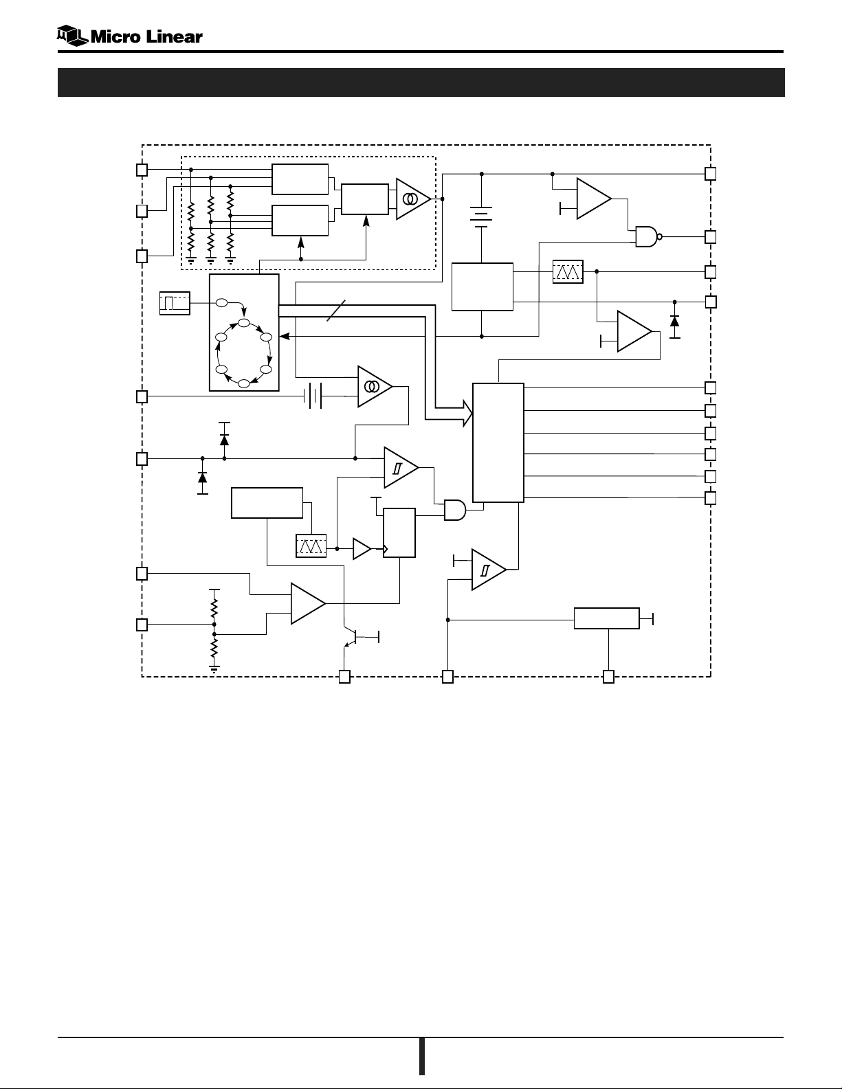
BLOCK DIAGRAM
FB A
14
FB B
15
FB C
16
COMMUTATION
STATE MACHINE
R
3µs
SPEED SET
SPEED COMP
ISENSE
SOFT START
POWER ON
RESET PULSE
5
3
1
19
F
E
8.2 + 0.7V
2.2 + 0.7V
1V
225kΩ
225kΩ
NEUTRAL
5.8kΩ
2.9kΩ
TRIANGLE WAVE
SIMULATOR
A
B
C
D
LEVEL SHIFT
GENERATOR
CURRENT LIMIT
COMPARATOR
MUX
SPEED FB
–
+
COMP
–
PRELIMINARY
SIGN
CHANGER
6
+
0.7V
+
–
BACK
EMF SAMPLER
SPEED
ERROR AMP
+
–
PWM
COMPARATOR
+
–
5V
DQ
R
VREF + 0.7V
+
–
VOLTAGE
CONTROLLED
OSCILLATOR
GATING
LOGIC
AND
OUTPUT
DRIVERS
PULSE-BY-PULSE
CURRENT LIMIT
8.7V
+
–
+
LEVEL
0.97V
SHIFT
0.7V
COAST
UVLO COMPARATOR
COMP
–
1.5V
6V REFERENCE
+
COMP
–
0.9V
VREF
ML4435
18
SPEED FB
2
TACH
20
CVCO
RVCO
4
7
HA
8
HB
9
HC
11
LA
12
LB
13
LC
6
RT VCC GND
1710
ML4435 Block Diagram
May, 2000 PRELIMINARY DATASHEET 3
PIN CONFIGURATION
PRELIMINARY
ML4435
20-P n PDIP P20
20-P n SOIC S20
ISENSE
TACH
SPEED COMP
RVCO
SPEED SET
RT
HA
HB
HC
VCC
2
3
4
5
6
9
0
TOP VIEW
20
9
6
5
4
3
2
CVCO
SOFT START
SPEED FB
ND
FB C
FB B
FB A
LC
LB
LA
ML4435
PIN DESCRIPTIONS
PIN NAME FUNCTION
1 ISENSE Motor current sense input which triggers pulse by pulse current limit when
ISENSE exceeds 0.55V
2 TACH A clock output of 6 pulses per commutation cycle when SPEED FB is greater
than 0.97V otherwise the TACH output is at 5V
3 SPEED COMP Connection node for speed loop compensation components
4 RVCO Connection node for external resistor to set VCO frequency
5 SPEED SET DC input for setting motor speed
6 RT External resistor from this pin to ground controls the IC's PWM timing (frequency)
7 HA High-side output driver for motor phase A
8 HB High-side output driver for motor phase B
9 HC High-side output driver for motor phase C
10 VCC Power Supply input
11 LA Low-side output driver signal for motor phase A
12 LB Low-side output driver signal for motor phase B
13 LB Low-side output driver signal for motor phase C
14 FB A Back EMF signal input for motor phase A
15 FB B Back EMF signal input for motor phase B
16 FB C Back EMF signal input for motor phase C
17 GND Signal and power ground
18 SPEED FB Connection node for back-EMF sensing compensation components
19 SOFT START Connection node for external soft start capacitor which reduces start up current
20 CVCO Connection node for external capacitor to set VCO frequency. Forcing this input
below 1.5V causes the commutation to stop and the motor to coast
PRELIMINARY DATASHEET
May, 20004
PRELIMINARY
FUNCTIONAL DESCRIPTION
ML4435
COMPONENT SELECTION
Selecting external components for the ML4435 requires
calculations based on the motor’s electrical and mechanical parameters. The following is a list of the motor parameters needed to for these calculations:
The maximum DC motor supply voltage V MOTOR (V)
The maximum operating current I MAX (A)
The winding resistance measured line to line Rl-l Ω
The number of magnetic poles N (Unitless)
The Back EMF constant Ke (V s/RAD)
The torque constant Kτ (N m/A) of the motor (Kτ = Ke
in SI units)
The maximum speed of operation RPMMAX (RPM)
The moment of inertia J (Kg m2 ) of the motor and its
load
The viscous damping factor ζ (Unitless) of the motor and
its load
If one or more of the above values is not known, it is
still possible to pick components for the ML4435, but
some experimentation may be necessary to determine the
optimal values. All quantities are in SI units unless otherwise specifi ed. The following formulas and component
selection graphs should be considered as a starting point
from which to optimize the application. All calculations
for capacitors and resistors should be used as the fi rst
approximation for selecting the closest standard value.
SUPPLY VOLTAGE AND ON-CHIP VOLTAGE
REFERENCE
OUTPUT DRIVERS
The output drivers LA, LB, LC, HA, HB, and HC provide
totem pole output drive signals for a 3 phase bridge power
stage. All control functions in the ML4435 translate to
outputs at these pins. LA, LB, LC provide the low side drive
signals for phases A, B, and C of the 3 phase power stage
and are 12V active high signals. HA, HB, and HC provide
the high side signals for phases A, B, and C of the 3 phase
power stage and are 12V active low signals.
CURRENT LIMITING IN THE 3 PHASE BRIDGE
POWER STAGE
A current sense resistor RSENSE shown in Figure 1 is
installed in the 3 phase power stage to regulate the maximum current in the power stage and the BLDC motor.
Current regulation is accomplished by shutting off the
output drivers LA, LB, and LC for the remainder of the
PWM period if the voltage across RSENSE exceeds the
current limit threshold set by the SOFT START (pin 19).
The maximum power dissipated in RSENSE is shown in
Figure 2.
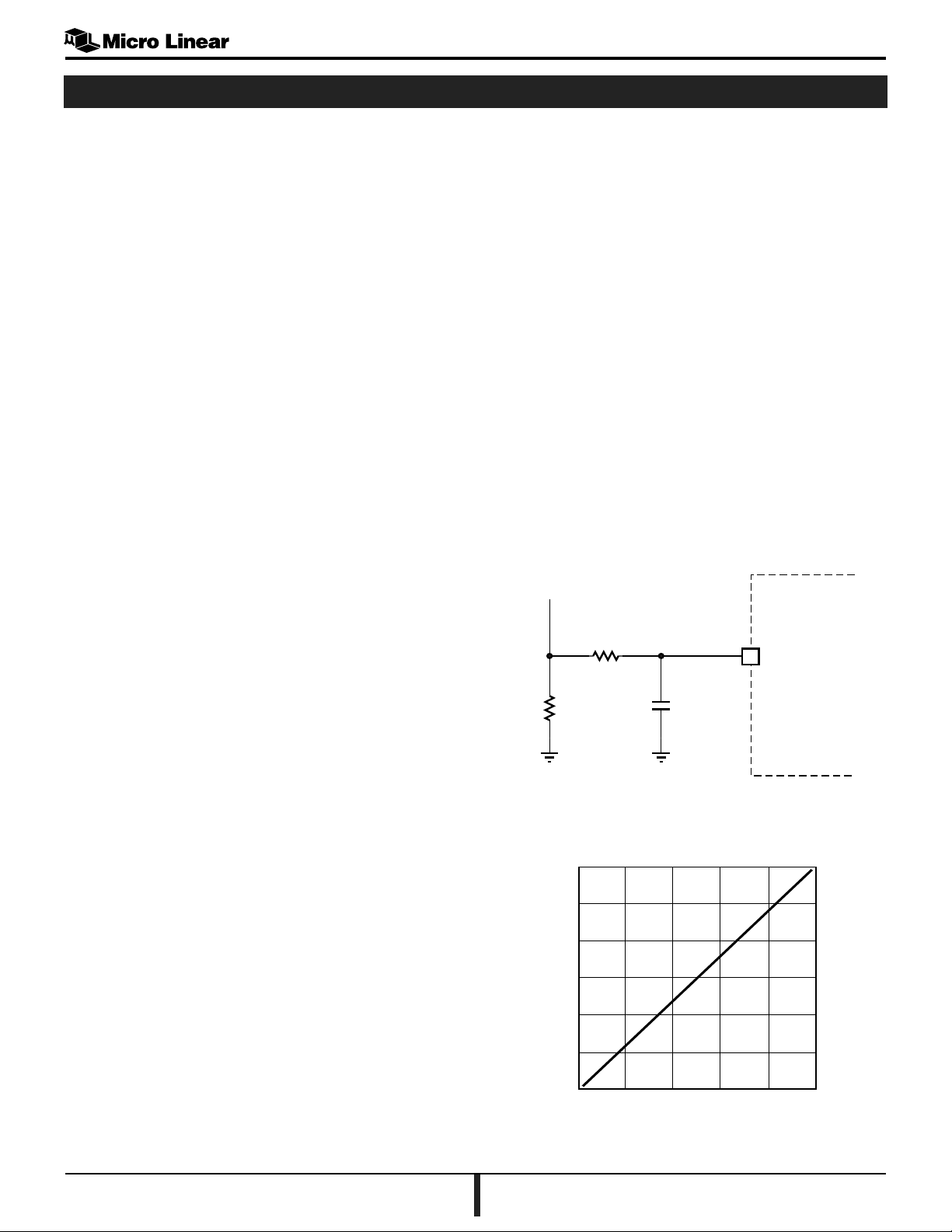
RSENSE
R
C
ISENSE
VCC
The supply voltage at VCC (pin 10) is nominally
12V ± 10%. A bypass capacitor of 0.1µF to ground as
close as possible to VCC (pin 10) is recommended.
RT
An internal 6V reference is generated inside the ML4435.
The reference appears on RT (pin 6). A resistor to ground
on RT sets the PWM frequency. This resistor can be
replace with a potentiomenter for use in setting the speed
command. This topic is discussed under the PWM SPEED
CONTROL section. Note: Buffer this pin with an op amp
with at least a 1MΩ input impedance if external circuits
are necessary.
May, 2000 PRELIMINARY DATASHEET 5
Figure 1. Current Limit with RSENSE
6
5
4
3
RSENSE Po er Rat n W
2
0
02
Figure 2. RSENSE Power vs. Motor Current
4
IMAX [MOTOR] A
60
 Loading...