

Micro Linear Corporation ML4411ACS, ML4411CS Datasheet
Sensorless Spindle Motor Controller
GENERAL DESCRIPTION
The ML4411 provides complete commutation for delta or
wye wound Brushless DC (BLDC) motors without the need
for signals from Hall Effect Sensors. This IC senses the
back EMF of the three motor windings (no neutral
required) to determine the proper commutation phase
angle using Phase Lock Loop techniques. This technique
will commutate virtually any 3-phase BLDC motor and is
insensitive to PWM noise and motor snubbing. The
ML4411 is architecturally similar to the ML4410 but with
improved braking and brown-out recovery circuitry.
Included in the ML4411 is the circuitry necessary for a
Hard Disk Drive microcontroller driven control loop.
The ML4411 controls motor current with either a constant
off-time PWM or linear current control driven by the
microcontroller. Braking and Power Fail are also included
in the ML4411.
The timing of the start-up sequencing is determined by the
micro, allowing the system to be optimized for a wide
range of motors and inertial loads.
May 1997
ML4411*/ML4411A**
The ML4411A includes a comparator on the P3 output to
prevent cross-conduction.
FEATURES
■ Back-EMF commutation provides maximum torque
for minimum “spin-up” time for spindle motors
■ Accurate, jitter-free phase locked motor speed
feedback output
■ Linear or PWM motor current control
■ Easy microcontroller interface for optimized start-up
sequencing and speed control
■ Power fail detect circuit with delayed braking
■ Drives external N-channel FETs and P-channel FETs
■ Back-EMF comparator detects motor rotation after
power fail for fast re-lock after brownout
The ML4411 modulates the gates of external N-Channel
power MOSFETs to regulate the motor current. The IC
drives P-Channel MOSFETs directly.
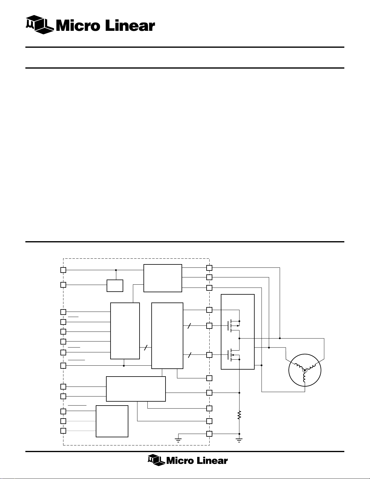
BLOCK DIAGRAM
RC
20
C
VCO
14
VCO/TACH OUT
15
RESET
16
I
RAMP
21
ENABLE E/A
18
BRAKE
26
DIS PWR
8
I
CMD
28
I
LIMIT
27
PWR FAIL
17
+5
19
VCC
25
VCO
LOGIC
AND
CONTROL
LINEAR OR PWM
CURRENT CONTROL
POWER
FAIL
DETECT
BACK-EMF
SAMPLER
GATE
DRIVE
6
* This Product Is Obsolete
** This Product Is End Of Life As Of August 1, 2000
PH1
22
PH2
23
PH3
24
POWER
DRIVERS
BLDC
MOTOR
PATENTED
3
3
VCC2
P1-3
N1-3
C
BRK
I
SENSE
C
C
OTA
GND
4
7
12
OS
13
6
1
1
ML4411/ML4411A
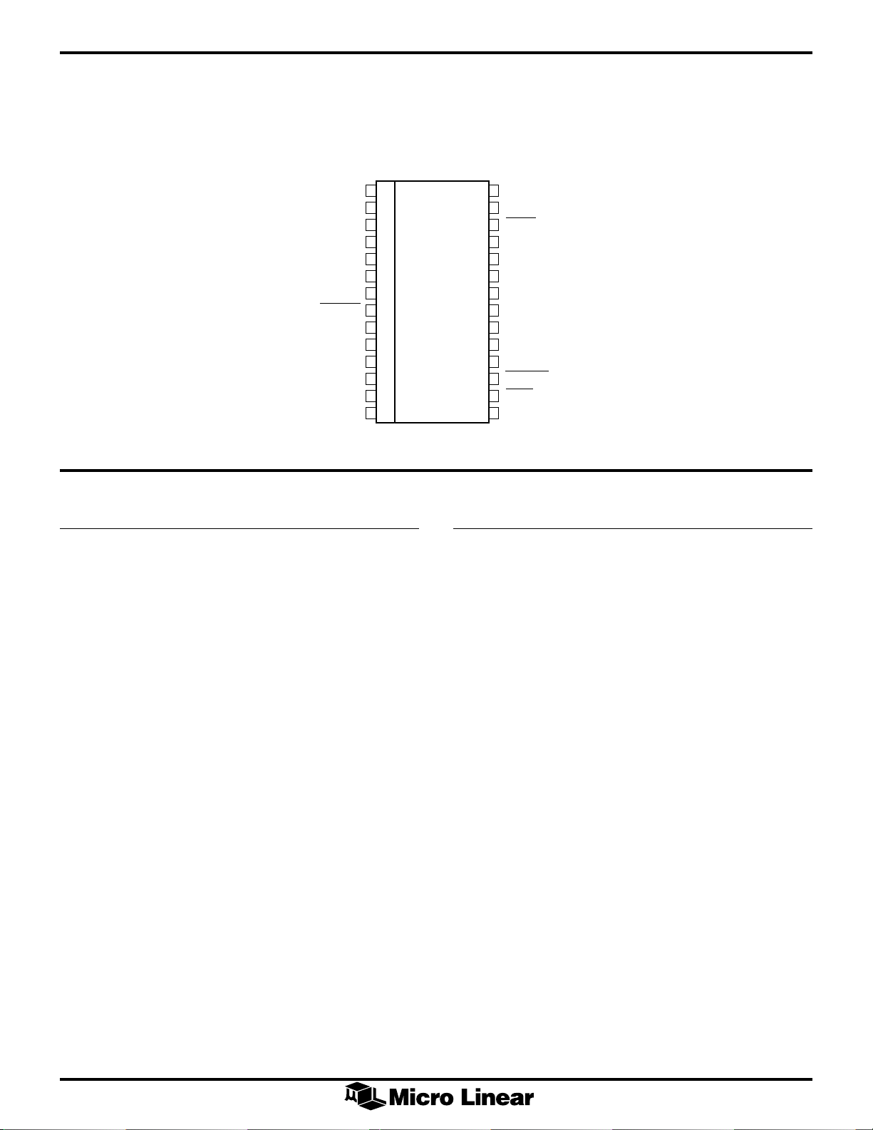
PIN CONFIGURATION
ML4411
28-Pin SOIC (S28W)
GND
VCC2
C
OTA
C
BRK
DIS PWR
N1
N2
N3
I
SENSE
C
C
VCO
1
P1
2
P2
3
4
P3
5
6
7
8
9
10
11
12
13
OS
14
TOP VIEW
I
28
I
27
BRAKE
26
VCC
25
PH3
24
PH2
23
PH1
22
I
21
RC
20
+5V
19
ENABLE E/A
18
PWR FAIL
17
RESET
16
VCO/TACH OUT
15
CMD
LIMIT
RAMP
PIN DESCRIPTION
PIN NAME FUNCTION PIN NAME FUNCTION
1 GND Signal and Power Ground
2 P1 Drives the external P-channel
transistor driving motor PH1
3 P2 Drives the external P-channel
transistor driving motor PH2
4V
CC2
12V power and power for the
braking function
5 P3 Drives the external P-channel
transistor driving motor PH3
6C
OTA
Compensation capacitor for linear
motor current amplifier loop
7C
BRK
Capacitor which stores energy to
charge N-channel MOSFETs for
braking with power off.
8 DIS PWR A logic 0 on this pin turns off the N
and P outputs and causes the TACH
comparator output to appear on TACH
OUT
9-11 N1, N2 N3 Drives the external N-channel
MOSFETs for PH1, PH2, PH3
12 I
13 C
SENSE
OS
Motor current sense input
Timing capacitor for fixed off-time
PWM current control
14 C
VCO
Timing capacitor for VCO
15 VCO/TACH Logic Output from VCO or TACH
OUT comparator
16 RESET Input which holds VCO off and sets the
IC to the RESET condition
17 PWR FAIL A “0” output indicates 5V or 12V is
under-voltage. This is an open
collector output with a 4.5ký pull-up
to +5V
18 ENABLE E/A A ”1” logic input enables the error
amplifier and closes the back-EMF
feedback loop
19 +5V 5V power supply input
20 RC VCO loop filter components
21 I
RAMP
Current into this pin sets the initial
acceleration rate of the VCO during
start-up
22 PH1 Motor Terminal 1
23 PH2 Motor Terminal 2
24 PH3 Motor Terminal 3
25 V
CC
12V power supply. Terminal which is
sensed for power fail
26 BRAKE A ”0” activates the braking circuit
27 I
LIMIT
Sets the threshold for the PWM
comparator
28 I
CMD
Current Command for Linear Current
amplifier
2
ML4411/ML4411A
ABSOLUTE MAXIMUM RATINGS
Absolute maximum ratings are those values beyond which
the device could be permanently damaged. Absolute
maximum ratings are stress ratings only and functional
device operation is not implied.
Supply Voltage (pins 4, 25) ........................................ 14V
OPERATING CONDITIONS
Temperature Range ........................................0°C to 70°C
VCC Voltage +12V (pin 25) ........................... 12V ± 10%
+5V (pin 19) ................................................ 5V ± 10%
I(RAMP) current (Pin 21)................................. 0 to 100µA
I Control Voltage Range (pins 27, 28) ................ 0V to 7V
Output Current (pins 2, 3, 5, 9,10,11) .................±150mA
Logic Inputs (pins 16, 17, 18, 25) .................... –0.3 to 7V
Junction Temperature ............................................ 150°C
Storage Temperature Range ..................... –65°C to 150°C
Lead Temperature (Soldering 10 sec.) .................... 150°C
Thermal Resistance (qJA) ...................................... 60°C/W
ELECTRICAL CHARACTERISTICS
Unless otherwise specified, TA = Operating Temperature Range, V
C
= 0.02µF
OS
PARAMETER CONDITIONS MIN TYP MAX UNITS
Oscillator (VCO) Section (V
Frequency vs. V
Frequency V
Reset Voltage at C
Sampling Amplifier (Note 1)
V
RC
I
RC
V
PIN21
Motor Current Control Section
I
Gain V
SENSE
One Shot Off Time 12 25 33 µs
I
Transconductance Gain 0.19 mmho
CMD
I
, I
CMD
LIM
Power Fail Detection Circuit
12V Threshold 9.1 9.8 10.5 V
Hysteresis 150 mV
5V Threshold 3.8 4.25 4.5 V
Hysteresis 70 mV
Logic Inputs
Voltage High (VIH)2V
Voltage Low (VIL) 0.8 V
Current High (IIH)V
Current Low (IIL)V
PIN 20
VCO
Bias Current VIN = 0 0 –100 –400 nA
PIN16
= 5V)
1V - V
VCO
V
VCO
Mode = 0 125 250 mV
State R 125 250 mV
V
PIN18
V
PIN18
V
PIN18
V
PIN18
R
PIN21
PIN27
= 2.7V –10 1 10 µA
IN
= 0.4V –500 –350 –200 µA
IN
- 10V 300 Hz/V
PIN20
= 6V 1450 1800 2150 Hz
= 0.5V 70 140 210 Hz
= 0V, R
= 5V, State A, V
= 5V, State A, V
= 5V, State A, V
= 39ký to +5V 1.0 1.1 1.20 V
= 5V, 0V - V
RAMP
PIN28
= V
CC
= 39ký 70 100 130 µA
= 4V 30 50 90 µA
PH2
= 6V –13 2 13 µA
PH2
= 8V –30 –50 –90 µA
PH2
- 2.5V 4.5 5 5.5 V/V
= 12V, R
CC2
SENSE
= 1ý, C
OTA
= C
VCO
= 0.01µF,
3
ML4411/ML4411A
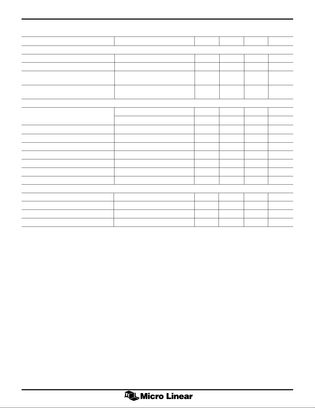
ELECTRICAL CHARACTERISTICS (Continued)
PARAMETER CONDITIONS MIN TYP MAX UNITS
Braking Circuit (V
Brake Active Threshold 0.8 1.2 1.6 V
PIN 26 Bias Current V
N-Channel Leakage V
Current VCC, V
C
BRK
Outputs (I
CMD
= I
IP Low VP = 0.8V 5 7 19.5 mA
VP High IP = –10µA VCC – 0.4 V
P3 Comparator Threshold V
VN High V
VN Low IN = 1mA 0.2 0.7 V
LOGIC Low (VOL)I
VCO/TACH V
OH
POWER FAIL V
Supply Currents (N and P Outputs Open)
5V Current 34mA
V
Current 38 50 mA
CC
V
Current ML4411 2 3 mA
CC2
V
Current ML4411A 2.6 3.75 mA
CC2
Note 1. For explanation of states, see Figure 5 and Table 1.
OH
PIN17
LIMIT
= 0V)
= 2.5V)
= 0V 0.3 1 µA
PIN26
, V
CC
V
PIN17
V
PIN7
V
= 0.4V 2 4 mA
P
PIN12
OUT
I
OUT
I
OUT
= 0V 0 0.06 10 nA
CC2
= 0V, VN = 4V
CC2
= 0V, V
= 3V 20 85 µA
PIN26
= 6V
= 0V V
– 1.6 V
CC2
– 3.2 10 VCC – 1.2 V
CC2
– 0.8 V
CC2
= 0.4mA 0.5 V
= –100µA 2.4 V
= –10µA V
PIN19
– 0.2 V
PIN19
– 0.1 V
PIN19
V
4
FUNCTIONAL DESCRIPTION
ML4411/ML4411A
The ML4411 provides closed-loop commutation for
3-phase brushless motors. To accomplish this task, a VCO,
integrating Back-EMF Sampling error amplifier and
sequencer form a phase-locked loop, locking the VCO to
the back-EMF of the motor. The IC also contains circuitry
to control motor current with either linear or constant offtime PWM modes. Braking and power fail detection
functions are also provided on chip. The ML4411 is
designed to drive external power transistors (N-channel
sinking transistors and PNP sourcing transistors) directly.
Start-up sequencing and motor speed control are
accomplished by a microcontroller. Speed sensing is
accomplished by monitoring the output of the VCO,
which will be a signal which is phased-locked to the
commutation frequency of the motor.
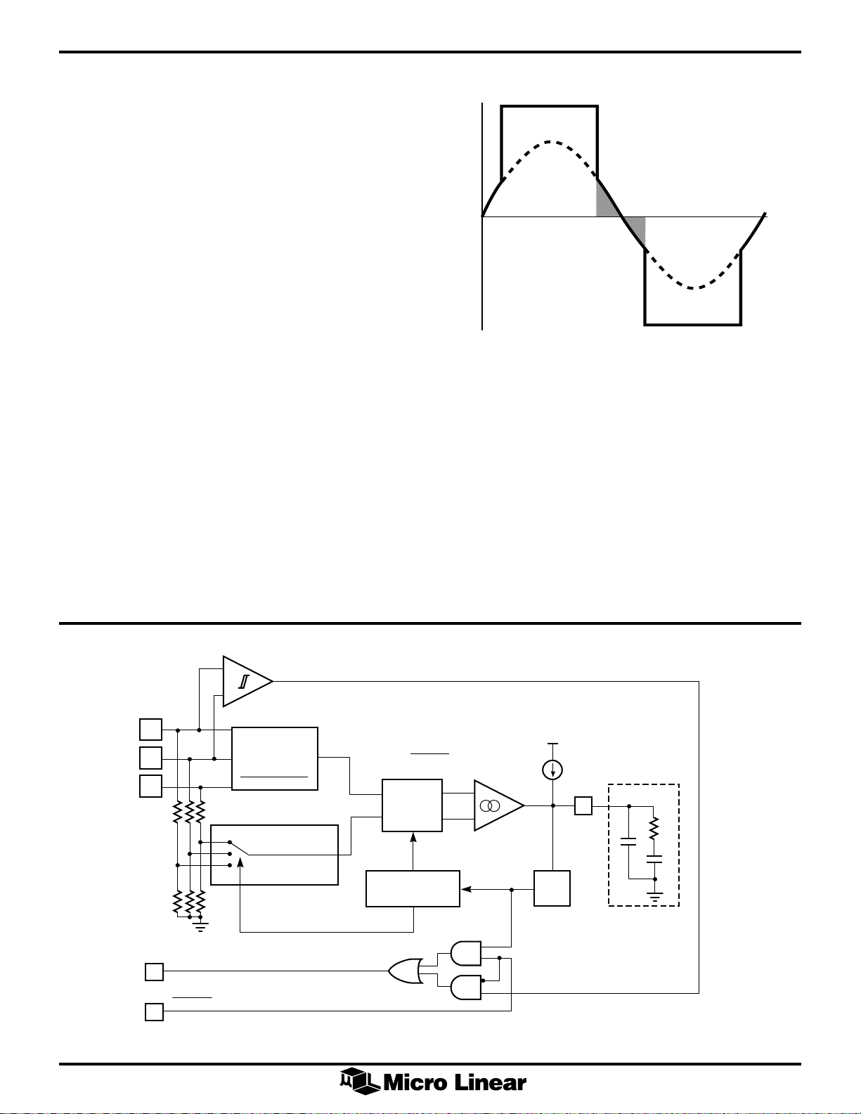
BACK-EMF SENSING AND COMMUTATOR
The ML4411 contains a patented back-EMF sensing
circuit which samples the phase which is not energized
(Shaded area in figure 2) to determine whether to increase
or decrease the commutator (VCO) frequency. A late
commutation causes the error amplifier to charge the
filter (RC) on pin 20, increasing the VCO input while
early
commutation causes pin 20 discharge. Analog speed
control loops can use pin 20 as a speed feedback voltage.
The input impedance of the three PH inputs is about 8Ký
to GND. When operating with a higher voltage motor, the
PH inputs should be divided down in voltage so that the
maximum voltage at any PH input does not exceed VCC.
NEUTRAL
0 60 120 180 240 0300
Figure 2. Typical motor phase waveform with Back-EMF
superimposed (Ideal Commutation)
VCO AND PHASE DETECTOR CALCULATIONS
The VCO should be set so that at the maximum frequency
of operation (the running speed of the motor) the VCO
control voltage will be no higher than VCC
– 1V. The
MIN
VCO maximum frequency will be:
F POLES RPM
=× ×005.
MAX
where POLES is the number of poles on the motor and
RPM is the maximum motor speed in Revolutions Per
ΦA
ΦB
ΦC
8K
8K
VCO /TACH OUT
DIS PWR
ROTATION
+
SENSE
–
NEUTRAL
SIMULATOR
ΦA + ΦB + ΦC
MULTIPLEXER
Va – Vb
=
I
RC
8K
6
SIGN
CHANGER
COMMUTATION
LOGIC
a
+
b
–
FIGURE 1. BACK EMKF sensing block diagram
+
I(PIN 21)
LOOP FILTER
RC
R
C1
C2
VCO
5
 Loading...