

Micro Linear Corporation ML2721DH Datasheet

PRELIMINARY
ML2721 Low IF Digital Cordless Transceiver
GENERAL DESCRIPTION
The ML2721 can be used as a single chip digital cordless
telephone transceiver or general purpose Frequency Shift
Keying (FSK) radio transceiver. It is designed to work in
the 902 to 928MHz ISM band under FCC Part 15
regulations. The device integrates all the frequency
generation, receive and transmit functions for data rates
up to 1.5Mbps. A complete radio only requires the
addition of an antenna switch. Micro Linear’s ML2751 is
an integrated 100mW power amplifier and receive LNA
with transmit/receive PIN diode drivers, and it can be
used with the ML2721 for extended range capability.
The ML2721 contains a proprietary low IF receiver with
all channel selectivity. An image reject mixer brings the
915MHz RF signal down to a low IF frequency of
1.024MHz. Then all IF filtering, IF gain, and
demodulation is performed at 1.024MHz. This provides all
the benefits of direct conversion to baseband and
minimizes the need for RF filtering. Also, the ML2721 can
operate with either a low cost LC filter or a SAW filter.
A single 1.83GHz synthesizer is used for both the receiver
LO and the transmitter. The ML2721 transmitter modulates
the VCO with filtered data, and a driver amplifier
provides typically 0dBm at 915MHz. The VCO and PLL
incorporate the resonator, the active devices, and the
tuning circuitry for a completely integrated function. An
internal post detection filter and data slicer are also
included.
FEATURES
n Single chip 900MHz Radio Transceiver
n Fully integrated filters for all IF, FM discriminator and
data filtering
n Image reject mixer & proprietary Low IF architecture
reduce the need for RF filtering
n Integrated 1.83GHz frequency synthesizer with internal
VCO resonator
n TX/RX calibration for max power transmission
n Modulation compensation for improved sensitivity
performance
n PLL Programmed via 3-wire interface
n DC regulation for 2.7V to 5.0V operation (IC
performance is reduced from 2.7V to 3.2V)
n PLL lock detect output
n Analog Received Signal Strength Indication (RSSI)
output to baseband IC
n Easily upgradable for extended range with ML2751
The ML2721 contains its own DC regulation which allows
the IC to operate over a wide power supply voltage range.
It also has a simple baseband interface for transmit power
management, PLL control and detection, and RSSI
(Receiver Signal Strength Indication).
PRELIMINARY DATASHEET
APPLICATIONS
n 900MHz DSSS cordless phones
n 900 to 930MHz radio transceivers with ranges from 10
feet to 1000 feet and data rates to 1.5Mbps
n Single IC 900MHz low power radio
n FCC Part 15 compliant radio links
n Portable computer/PDA
n TDD and TDMA radios
January, 2000

PRELIMINARY
ML2721
TABLE OF CONTENTS
General Description ................................................................................................................................................... 1
Features...................................................................................................................................................................... 1
Applications ............................................................................................................................................................... 1
Simplified Block Diagrams......................................................................................................................................... 3
Block Diagram ........................................................................................................................................................... 4
Pin Configuration ....................................................................................................................................................... 5
Pin Descriptions ......................................................................................................................................................... 5
Functional Description ............................................................................................................................................... 8
Introduction.............................................................................................................................................................. 8
Circuit Block Descriptions........................................................................................................................................ 8
Modes Of Operation .................................................................................................................................................. 10
Overview ................................................................................................................................................................. 10
Receive Modes ........................................................................................................................................................ 10
Transmit Mode ......................................................................................................................................................... 12
Standby Mode .......................................................................................................................................................... 15
Test Mode ................................................................................................................................................................ 15
Control Interfaces ....................................................................................................................................................... 16
Register Information ................................................................................................................................................. 17
Transmit and Receive Data Interfaces ...................................................................................................................... 22
Applications ............................................................................................................................................................... 23
Electrical Characteristics............................................................................................................................................ 24
Electrical Tables ......................................................................................................................................................... 24
Absolute Maximum Ratings........................................................................................................................................ 24
Operating Conditions ................................................................................................................................................. 24
Physical Dimensions .................................................................................................................................................. 28
Ordering Information .................................................................................................................................................. 28
WARRANTY
Micro Linear makes no representations or warranties with respect to the accuracy, utility, or completeness of the contents
of this publication and reserves the right to make changes to specifications and product descriptions at any time without
notice. No license, express or implied, by estoppel or otherwise, to any patents or other intellectual property rights is
granted by this document. The circuits contained in this document are offered as possible applications only. Particular uses
or applications may invalidate some of the specifications and/or product descriptions contained herein. The customer is
urged to perform its own engineering review before deciding on a particular application. Micro Linear assumes no liability
whatsoever, and disclaims any express or implied warranty, relating to sale and/or use of Micro Linear products including
liability or warranties relating to merchantability, fitness for a particular purpose, or infringement of any intellectual property
right. Micro Linear products are not designed for use in medical, life saving, or life sustaining applications.
© Micro Linear 2000. is a registered trademark of Micro Linear Corporation. All other trademarks are the property of their
respective owners.
Products described herein may be covered by one or more of the following U.S. patents: 4,897,611; 4,964,026; 5,027,116;
5,281,862; 5,283,483; 5,418,502; 5,508,570; 5,510,727; 5,523,940; 5,546,017; 5,559,470; 5,565,761; 5,592,128; 5,594,376;
5,652,479; 5,661,427; 5,663,874; 5,672,959; 5,689,167; 5,714,897; 5,717,798; 5,742,151; 5,747,977; 5,754,012; 5,757,174;
5,767,653; 5,777,514; 5,793,168; 5,798,635; 5,804,950; 5,808,455; 5,811,999; 5,818,207; 5,818,669; 5,825,165; 5,825,223;
5,838,723; 5.844,378; 5,844,941. Japan: 2,598,946; 2,619,299; 2,704,176; 2,821,714. Other patents are pending.
2
PRELIMINARY DATASHEET
January, 2000
PRELIMINARY
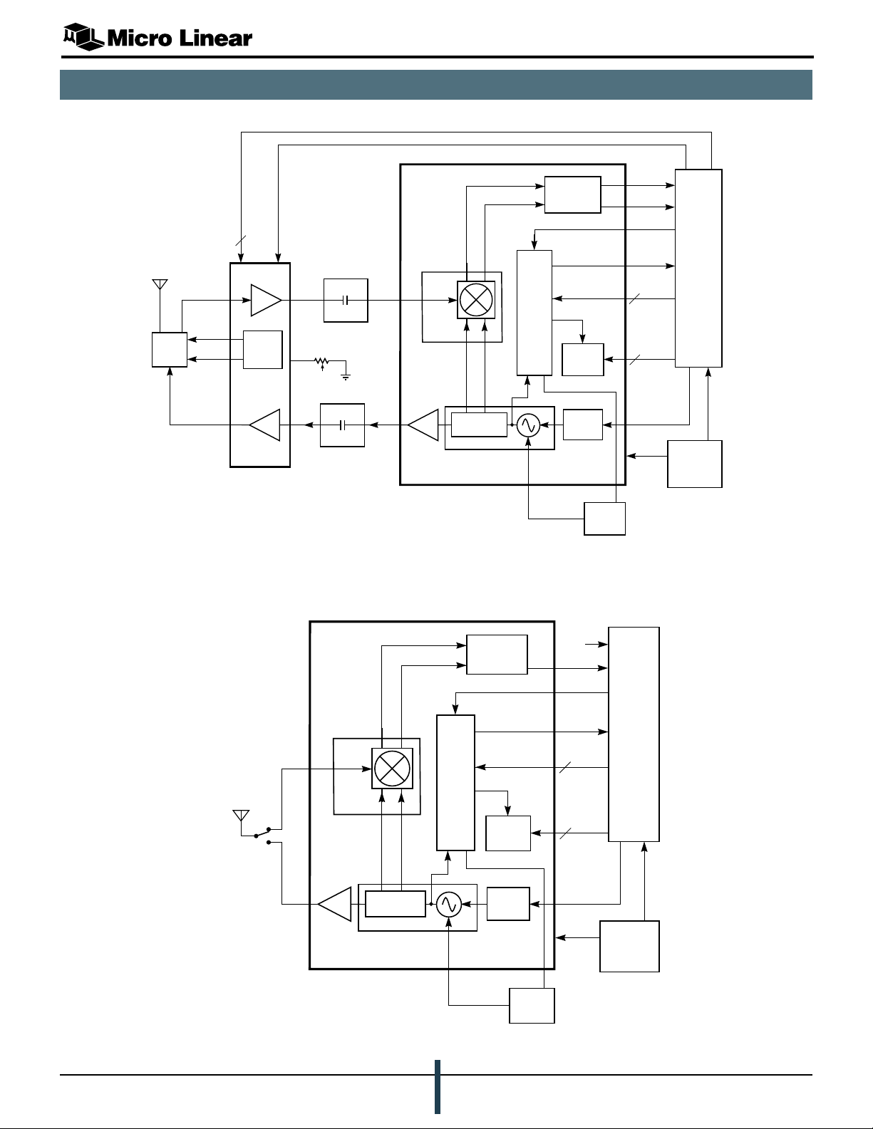
SIMPLIFIED BLOCK DIAGRAMS
ML2721
ANTENNA
RF PIN
DIODE
SWITCH
PINB
PIN
FEEN
2
PAON
ML2751
SWITCH
DRIVERS
TX RF
PA + DRIVER
QPO
LOOP
FILTER
DOUT
RSSI
REF
LD
3
3
DIN
VCCA
CLK,
DATA,
EN
XCEN,
RXON,
PLLEN
BASEBAND
IC
BATTERY
AND
PROTECTION
CIRCUITS
ML2721
TPS
RRFO
RF
TPA
TRFI
LC
FILTER
LC
FILTER
RRFI
TRFO
TX RF
BUFFER
IMAGE
REJECT
MIXER
QUADRATURE
DIVIDE BY 2
1.83GHz VCO
PLL
VTUNE
IF CIRCUITS
CONTROL
LOGIC
TX DATA
FILTER
900MHz DSSS Cordless Phone Application
ANTENNA
RRFI
TRFO
ML2721
IMAGE
REJECT
MIXER
TX RF
BUFFER
QUADRATURE
DIVIDE BY 2
1.83GHz VCO
PLL
VTUNE
IF CIRCUITS
CONTROL
LOGIC
TX DATA
FILTER
QPO
LOOP
FILTER
DOUT
RSSI
REF
LD
3
3
DIN
VCCA
CLK,
DATA,
EN
XCEN,
RXON,
PLLEN
BASEBAND
IC
BATTERY
AND
PROTECTION
CIRCUITS
General Purpose FSK Radio
January, 2000
PRELIMINARY DATASHEET
3
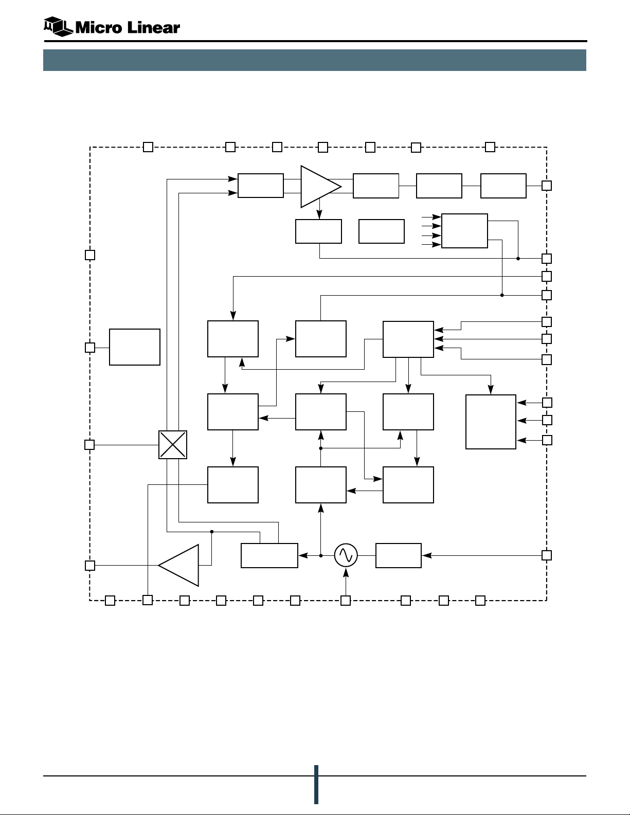
BLOCK DIAGRAM
PRELIMINARY
ML2721
VBG
VCC
RRFI
VDD
31
26
24
5
21
DC
REGULATORS
RX
QUADRATURE
MIXERS
Q
I
RVCC
1
10
REFERENCE
DIVIDER
LO PHASE/
FREQUENCY
DETECTOR
IF
FILTER
RVCC
14
3
RVCC
22
LIMITER
RSSI
LOCK
DETECT
LO 6-BIT
COUNTER
TEST
MUX
VCC
2
13
DATA
SLICER
CONTROL
LOGIC
DOUT
32
RSSI
28
9
REF
7
LD
EN
4
5
DATA
6
CLK
XCEN
1
2
RXON
3
PLLEN
RVCC
4
27
DEMOD
FILTER
ALIGN
6
ADDRESS
DECODE
LO 6-BIT
SWALLOW
COUNTER
RVCC
29
7
DATA
FILTER
TRFO
Q
GND
PRESCALAR
32 / 33
18
1.83GHz VCO
15
VTUNE
PRESCALAR
CONTROL
TX DATA
FILTER
19
GND
20
GND
25
GND
30
DIN
LO CHARGE
PUMP
TX RF
BUFFER
23
8
VSS
11
QPO
LIMITER
12
GND
16
GND
I
QUADRATURE
DIVIDE BY 2
17
GND
4
PRELIMINARY DATASHEET
January, 2000
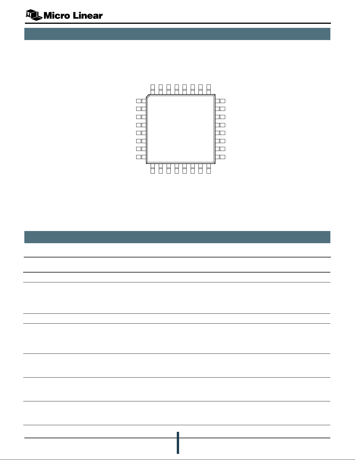
PIN CONFIGURATION
PRELIMINARY
ML2721
32-Pin TQFP (H32-7)
DOUT
VDD
DIN
RVCC7RSSI/TPI
RVCC6VBG
GND
ML2721
XCEN
RXON
PLLEN
EN
DATA
CLK
LD/TPQ
VSS
32 31 30 29 28 27 26 25
1
2
3
4
5
6
7
8
9 10111213141516
REF
1
RVCC
QPO
TOP VIEW
GND
2
VCC
3
RVCC
VTUNE
24
23
22
21
20
19
18
17
GND
VCC
TRFO
RVCC
RRFI
GND
GND
GND
GND
PIN DESCRIPTIONS
Pin # Signal Name I/O Description
5
4
Power & Ground
13 VCC
24 VCC
2
5
16 GND I (analog) DC ground for VCO and LO circuits
10 RVCC
14 RVCC
22 RVCC
27 RVCC
1
3
4
6
I (analog) DC Power Supply Input to the VCO voltage regulator
I (analog) DC power supply Input to Voltage Regulators and unregulated loads:
2.7 to 5.0V. VCC5 is the main (or master) analog VCC pin. There must
be a capacitor to ground from this pin to decouple (bypass) noise and
to stabilize the regulator
O (analog) DC power supply decoupling point for the PLL dividers, phase detector,
and charge pump. This pin is connected to the output of the regulator
and to the PLL supplies. There must be a capacitor to ground from this
pin to decouple (bypass) noise and to stabilize the regulator
O (analog) DC power supply decoupling point for the VCO. Connected to the
output of the VCO regulator. There must be a capacitor to ground from
this pin to decouple (bypass) noise and to stabilize the regulator
O (analog) DC power supply decoupling point for the LO Chain. Connected to the
output of a regulator. There must be a capacitor to ground from this pin
to decouple (bypass) noise and to stabilize the regulator
O (analog) DC power supply decoupling point for Quadrature Mixer and IF filter
circuits. There must be a capacitor to ground from this pin to decouple
(bypass) noise and to stabilize the regulator
January, 2000
PRELIMINARY DATASHEET
5

PRELIMINARY
PIN DESCRIPTIONS (continued)
Pin # Signal Name I/O Description
Power & Ground (Continued)
ML2721
29 RVCC
25 GND I (analog) DC Ground to IF, Demodulator, and Data Slicer circuits
12 GND I (analog) Ground for the PLL dividers, phase detector, and charge pump
17 GND I (analog) Signal ground for RF small signal circuits. Pins 17, 18, and 19 should
18 GND I (analog) Ground return for the Receive RF input
19 GND I (analog) Signal ground for the Receive mixers
20 GND I (analog) DC and Signal ground for the Transmit RF Output buffer
31 VDD I (analog) DC power supply input to the interface logic and control registers. This
8 VSS I (digital) Ground for digital I/O circuits and control logic
7
O (analog) DC power supply decoupling point for IF, Demodulator, and Data
Slicer circuits. There must be a capacitor to ground from this pin to
decouple (bypass) noise and to stabilize the regulator
have short, direct connections to each other and additional
connections to ground
supply is not internally connected to any other supply pin, but its
voltage must be less than or equal to the VCC5 supply, and greater
than 2.7V. There must be a capacitor to ground from this pin to
decouple (bypass) noise and to stabilize the regulator
Transmit/Receive
21 RRFI I (analog) Receive RF Input. Nominal impedance at 902 to 928MHz is 50W, with
a simple matching network required for optimum noise figure. This
input is to the base of an NPN transistor and should be AC coupled
23 TRFO O (analog) Transmit RF Output. A broadband 50W output which sources 0dBm
over the 902 to 928MHz range. This output is an emitter follower and
should be AC coupled
Data
30 DIN I (CMOS) Transmit Data input. Drives the transmit pulse shaping circuits. Serial
digital data on this pin becomes FSK modulation on the Transmit RF
output. Data timing is controlled by the logic timing on this pin. The
modulation deviation is determined by internal circuits. This is a
standard CMOS input referenced to VDD &VSS
32 DOUT O (CMOS) Serial digital output after demodulation, chip rate filtering and center
data slicing. A CMOS level output (VSS to VDD) with controlled slew
rates. A low drive output designed to drive a PCB trace and a CMOS
logic input while generating minimal RFI. In digital test modes this pin
becomes a test access port controlled by the serial control bus
Mode Control and Interface Lines
1 XCEN I (CMOS) Enables the bandgap reference and voltage regulators when high.
Consumes only leakage current in standby mode when low. This is a
CMOS input, and the thresholds are referenced to VDD & VSS
2 RXON I (CMOS) Switches the transceiver between Transmit and Receive modes.
Circuits are powered up and signal paths reconfigured according to the
operating mode. This is a CMOS input, and the thresholds are
referenced to VDD & VSS
6
PRELIMINARY DATASHEET
January, 2000

PRELIMINARY
PIN DESCRIPTIONS (continued)
Pin # Signal Name I/O Description
Mode Control and Interface Lines (Continued)
3 PLLEN I (CMOS) Enables the PLL at the beginning of a Transmit or Receive slot. Goes
low before data is received or transmitted. RXON and PLLEN define
four distinct operating modes. This is a CMOS input, and the thresholds
are referenced to VDD & VSS
7 LD/TPQ O (CMOS) The Lock Detect output is an open drain output that goes low when the
PLL is in frequency lock. In analog test modes this pin and the RSSI
output become test access points controlled by the serial control bus
9 REF I Input for the 6.144MHz or 12.288MHz reference frequency. This is
used as the reference frequency for the PLL, and as a calibration
frequency for the on chip filters. This is a self-biased CMOS input that
is designed to be driven either by a an AC coupled sine wave source
(recommended coupling capacitor is 470pF) or by a standard CMOS
output
11 QPO O Charge Pump Output of the phase detector. This is connected to the
external PLL loop filter
15 VTUNE I VCO Tuning Voltage input from the PLL loop filter. This pin is very
sensitive to noise coupling and leakage currents
ML2721
26 VBG O Bandgap reference voltage. Decoupled to ground with a 220nF
capacitor
28 RSSI/TPI O Buffered Analog RSSI output with a nominal sensitivity of 33mV/dB.
An RF input signal range of –95 to –15dBm gives an RSSI voltage
output of zero to 2.7V. In analog test modes this pin and the LD output
become test access ports
Serial Bus Signals
4 EN I (CMOS) Enable pin for the three wire serial control bus which sets the
operating frequency and programmable options. The control registers
are loaded on a low to high transition of the signal. Serial control bus
data is ignored when it is high. This is a CMOS input, and the
thresholds are referenced to VDD & VSS
5 DATA I (CMOS) Serial control bus data. 16 bit words which include programming data
and the two bit address of a control register. This is a CMOS input, and
the thresholds are referenced to VDD & VSS
6 CLK I (CMOS) Serial control bus data is clocked in on the rising edge when EN is
low. This is a CMOS input, the thresholds are referenced to VDD & VSS
January, 2000
PRELIMINARY DATASHEET
7
PRELIMINARY
FUNCTIONAL DESCRIPTION
ML2721
INTRODUCTION
The ML2721 enables the design and manufacture of low
cost, high performance digital DSSS cordless telephone
transceivers. It can also be used as a general purpose
900MHz transceiver. Integral to the ML2721 is a low IF
receiver whose LO port is driven from an internal
synthesizer. Included are image rejection IF filters,
limiters, discriminator, data slicers, and baseband lowpass
data filters. It also contains internal voltage regulators to
protect critical circuits from power supply noise and
transmit modulation circuits.
The ML2721 has an internal control interface that
programs the synthesizer, the mode of operation, the
external LNA and PA, and provides a convenient and
flexible interface to various baseband processors. For
power level monitoring an RSSI block is included.
The ML2721 is designed to transmit and receive
1.536Mchips signals in 2.048MHz spaced channels in the
902 to 928MHz ISM band. The 1.536Mchips rate with a
15 bit spreading code gives a 102.4kb/s data rate and
provides a 10dB processing gain.
In the Receive mode the ML2721 is a single conversion
low IF receiver. The IF frequency of 1.024MHz results in
an image response in an adjacent channel. An image
reject mixer gives sufficient rejection in this channel. All
IF filtering and demodulation is performed using active
filtering, centered at 1.024MHz. The demodulator is
followed by a matched bit rate filter and a data slicer. The
sliced data is provided to a baseband chip for despreading.
CIRCUIT BLOCK DESCRIPTIONS
PHASE LOCKED LOOP (PLL) AND VOLTAGE
CONTROLLED OSCILLATOR (VCO)
The PLL synthesizes channel frequencies to a 512kHz
resolution, which is more finely spaced than the
1.536MHz signal bandwidth. Non-overlapping channels
are spaced by 2.048MHz where the IF filter and image
reject mixer give a typical adjacent channel rejection of
25dB. There are twelve non-overlapping channels in the
902 to 928MHz ISM band. See Table 1.
lennahCzHMniycneuqerF
1086.309
2827.509
3677.709
4428.909
5278.119
6029.319
7869.519
8610.819
9460.029
01211.229
11061.429
21802.629
Table 1. Non-Overlapping Channel Frequencies
In the Transmit mode the ML2721 uses the Receive mode
VCO and frequency division, with a driver amplifier
providing typically 0dBm output to feed the power
amplifier. The PLL frequency synthesizer loop is opened
during the transmit slot, and the VCO is directly
modulated by low-pass filtered circuits from the internal
modulation filter.
The frequency generation circuits are an internal VCO at
1.83GHz, dividers, a phase comparator and a charge
pump for a PLL frequency synthesizer. The VCO output is
divided by two to produce accurate quadrature outputs at
915MHz. No external components are need for the VCO.
Other modes that are available include power down, and
receive and transmit calibrate, which are discussed in
further detail.
The LO PLL is programmed via a 3-wire serial control bus.
Program words are clocked in on the DATA line (pin 5) by
the CLK (pin 6), and loaded into the dividers or control
circuits when EN (pin 4) is asserted. There is no check for
error in the program words. Once loaded, register contents
are preserved regardless of power conditions. The register
status and operation is independent of the mode of
operation of the PLL.
The reference signal from an external crystal oscillator at
either 6.144MHz or 12.288MHz is fed to a programmable
reference divider. The 1.024MHz reference divider output
is fed to the LO phase frequency detector. The PLL
prescaler input comes from the VCO at 1.83GHz, so the
1.024MHz comparison frequency gives 512kHz frequency
resolution at 902 to 928MHz.
The output of the LO divider is fed to the LO phase/
frequency detector and subsequently to the charge pump.
The dividers and charge pump are disabled during the
active slot to save power.
8
PRELIMINARY DATASHEET
January, 2000

PRELIMINARY
CIRCUIT BLOCK DESCRIPTIONS
ML2721
LO VCO AND TRANSMIT DRIVER
The internal LO VCO operates at 1.8 to 1.86GHz, which
is two times the LO frequency of 900 to 930MHz. The
VCO output is divided by 2 to give accurately matched
quadrature signals at 915MHz. In Receive mode the LO is
offset from the wanted signal by +1.024MHz to produce
the low IF. This 1.024MHz shift is produced by
automatically adding an offset of +2 counts to the PLL
divider programming.
In Transmit mode the LO is frequency modulated by the
transmitted data, using a modulation port of the VCO. The
VCO output is divided by 2 and a driver amplifier
typically develops 0dBm at 900 to 930MHz to directly
drive an ML2751 power amplifier.
TRANSMIT DATA FILTER AND MODULATION DRIVER
Logic level NRZ signals at DIN are scaled and filtered by
th
a 5
-order lowpass filter. The lowpass filter is tuned to
give a 1.35MHz 3dB point to pass the 1.536Mchips
transmit data. The filter data is then fed to the internal
modulation port of the LO tank circuit.
In the transmit closed loop mode the modulation port is
held at its midpoint so that the synthesizer locks to the
center channel frequency. In the transmit open loop mode
the VCO is modulated by Gaussian filtered data via the
VCO modulation port. The modulation driver contains
scaling circuitry to control the FM deviation over the
entire VCO tuning range. This circuit is inactive in the
receive mode.
DATA FILTER AND DATA SLICER
The FM demodulator is followed by a Gaussian lowpass
filter whose 768kHz cutoff frequency is matched to the
transmitted 1.536Mchip/s waveform. This Gaussian filter is
implemented with similar circuits to the IF filter, and is
shared with the Transmit modulation path. The filter output
can be AC coupled to the slicer because the spreading
code is almost DC balanced. The data slicer signal is
output to the baseband processor for timing recovery and
decoding.
POWER SUPPLY
The ML2721 uses multiple voltage regulators to protect
sensitive internal circuits from power supply noise.
Separate regulators supply the PLL dividers, RF circuits
and IF circuits. Each of these regulators takes its power
from VCC5, and supplies power internally to its respective
RVCCn pin. External capacitors are required at each
RVCCn pin to decouple the outputs of the internal
regulators. The VCO regulator takes its power from the
VCC2 pin which is normally connected to the RVCC6 pin.
An external decoupling capacitor is also used on the
internal bandgap voltage reference to improve the noise
performance of the regulators.
These regulators are effective at supply voltages from
3.0V to 5.0V. As the VCC5 supply voltage drops below
3.0V chip performance gradually degrades, but the
ML2721 transceiver will maintain the link as long as the
supply voltage is greater than 2.7V.
RECEIVE MIXERS AND IF CHAIN
The Receive RF quadrature mixers down-convert the
signal to the 1.024MHz receiver IF. The input of the mixer
is single-ended and matched to 50W by a series inductor.
This gives a good terminating impedance for the
preceding RF filter. The quadrature outputs of the down
converter feed the IF filter. The quadrature mixer and IF
filter together achieve a typical image rejection of 35dB.
A quadrature combiner for the image reject mixer and a
12th-order Gaussian bandpass filter make up the active IF
filters. The active filters provide an accurate Gaussian
characteristic with a 1.408MHz, 3dB bandwidth which
improves both sensitivity and adjacent channel rejection.
The IF amplifiers provide the bulk of the receiver’s gain.
An RSSI signal is generated by using the outputs of the IF
amplifiers. The RSSI signal is conditioned and sent to the
baseband controller. A frequency-to-voltage converter
provides highly linear FM demodulation with good data
recovery from the low IF.
January, 2000
PRELIMINARY DATASHEET
9
 Loading...