

Micro Linear Corporation ML2713CH, ML2713EH Datasheet

PRELIMINARY
ML2713 Radio IF Transceiver
GENERAL DESCRIPTION
The ML2713 combined with the ML2712 forms an
FSK (Frequency Shift Keying) 2.4 GHz radio chipset
for systems based on IEEE802.11 and other wireless
communication protocols using the 2.4HGz ISM band.
The ML2713 is the complete IF section of Micro Linear’s
2.4GHz frequency hopping, half duplex radio transceiver
chipset. The chip’s down conversion super-heterodyne
receiver circuit contains an image reject down-convert
mixer, a limiter, a discriminator, a receive data filter and
a tracking A/D converter. The chips transmit circuit
contain a 6 bit D/A converter to digitally modulate the IF,
an anti alias filter and an image reject up-convert mixer.
APPLICATIONS
n 2.4GHz FSK radios
n PC Card and FlashCard Wireless Transceivers
n Systems based on IEEE802.11 1Mbps and 2Mbps
Standard
n TDMA Radio IF circuits
FEATURES
n Highly integrated IF transceiver
n Data rates up to 4Mbps
n Integrated discriminator and filter alignment circuits
n High signal to noise ratio at the discriminator output
n Received signal strength indicator (RSSI)
n D/A Converter for digitally generated IF
n Low sleep mode current - typically less than 1mA
n 3.0V to 5.5V operation
n Fast 10msec switch time between transmit and receive
modes
n 48 Pin TQFP, 7mm body
SIMPLIFIED BLOCK DIAGRAM
1
3
7
2
L
M
s
ia
B
r
lle
tro
n
o
C
T
n
a
i
r
t
s
m
P
o
w
r
e
p
A
m
l
i
f
i
r
e
.
R
C
.
o
L
o
p
F
i
l
t
r
e
ML2712
Tx Regulator
Output
2
o
L
O
L
o
p
F
i
l
t
&
r
e
T
n
a
k
C
u
c
i
r
i
t
1
o
L
O
L
o
p
F
i
l
t
&
r
e
T
n
a
k
C
u
c
i
r
i
t
3
2
M
C
l
o
2LO
Input
j
e
e
g
a
t
c
R
e
I
x
m
R
I
F
D
o
w
n
o
c
n
t
r
e
v
r
e
3
1
7
2
L
M
j
e
e
g
a
t
c
R
e
I
m
T
x
I
F
U
p
o
c
n
t
r
e
v
r
D
e
R
e
C
g
(e
n
e
f
e
e
r
c
R
e
q
e
F
r
u
n
e
c
y
I
n
p
u
t
H
z
c
k
D
RSSI
Limiter
A
C
o
n
C
c
i
r
C
o
n
o
t
r
l
I
n
f
e
c
t
a
r
e
d
n
a
b
se
a
B
r
lle
tro
n
o
C
., M
.g
i
i
m
s
r
c
i
n
t
a
o
r
u
d
Q
a
&
F
i
l
t
r
e
u
t
o
A
l
i
g
o
t
r
l
u
i
t
s
)
B
0
3
7
7
M
S
-
D
t
a
a
F
i
l
t
r
e
n
D
A
C
D
/
A
I
n
p
u
t
3
6
D
C
s
e
t
R
o
e
r
u
x
R
O
t
+
–
PRELIMINARY DATASHEET
January, 2000

PRELIMINARY
ML2713
TABLE OF CONTENTS
General Description ................................................................................................................................................... 1
Applications ............................................................................................................................................................... 1
Features...................................................................................................................................................................... 1
Simplified Block Diagram .......................................................................................................................................... 1
Block Diagram ........................................................................................................................................................... 3
Pin Configuration ....................................................................................................................................................... 4
Pin Descriptions ......................................................................................................................................................... 4
Functional Description ............................................................................................................................................... 7
Introduction.............................................................................................................................................................. 7
Operational Modes .................................................................................................................................................. 8
Mode Control ........................................................................................................................................................... 8
Filter Align Mode..................................................................................................................................................... 8
Receive Mode ......................................................................................................................................................... 12
Sleep Mode.............................................................................................................................................................. 14
Test Mode Control .................................................................................................................................................... 14
Absolute Maximum Ratings........................................................................................................................................ 15
Electrical Characteristics............................................................................................................................................ 15
Operating Conditions ................................................................................................................................................. 15
Physical Dimensions .................................................................................................................................................. 20
Ordering Information .................................................................................................................................................. 20
WARRANTY
Micro Linear makes no representations or warranties with respect to the accuracy, utility, or completeness
of the contents of this publication and reserves the right to make changes to specifications and product
descriptions at any time without notice. No license, express or implied, by estoppel or otherwise, to any
patents or other intellectual property rights is granted by this document. The circuits contained in this
document are offered as possible applications only. Particular uses or applications may invalidate some of
the specifications and/or product descriptions contained herein. The customer is urged to perform its own
engineering review before deciding on a particular application. Micro Linear assumes no liability
whatsoever, and disclaims any express or implied warranty, relating to sale and/or use of Micro Linear
products including liability or warranties relating to merchantability, fitness for a particular purpose, or
infringement of any intellectual property right. Micro Linear products are not designed for use in medical,
life saving, or life sustaining applications.
© Micro Linear 2000. is a registered trademark of Micro Linear Corporation. All other trademarks are the
property of their respective owners.
Products described herein may be covered by one or more of the following U.S. patents: 4,897,611;
4,964,026; 5,027,116; 5,281,862; 5,283,483; 5,418,502; 5,508,570; 5,510,727; 5,523,940; 5,546,017;
5,559,470; 5,565,761; 5,592,128; 5,594,376; 5,652,479; 5,661,427; 5,663,874; 5,672,959; 5,689,167;
5,714,897; 5,717,798; 5,742,151; 5,747,977; 5,754,012; 5,757,174; 5,767,653; 5,777,514; 5,793,168;
5,798,635; 5,804,950; 5,808,455; 5,811,999; 5,818,207; 5,818,669; 5,825,165; 5,825,223; 5,838,723;
5.844,378; 5,844,941. Japan: 2,598,946; 2,619,299; 2,704,176; 2,821,714. Other patents are pending.
2
PRELIMINARY DATASHEET
January, 2000
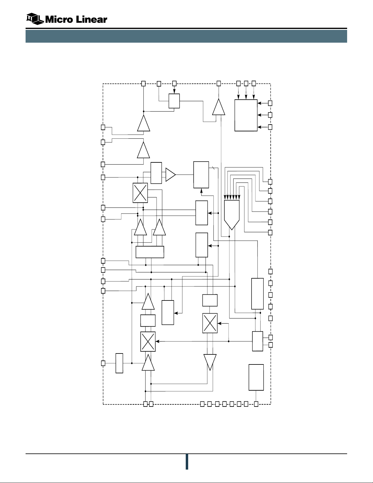
BLOCK DIAGRAM
V
A
R
I
A
B
L
E
C
A
P
A
C
I
T
O
R
A
R
R
A
Y
1
I
F
1
I
F
B
3
2
R
E
G
R
e
c
e
i
v
e
I
m
a
g
e
R
e
j
e
c
t
D
o
w
n
-
C
o
n
v
e
r
t
M
i
x
e
r
T
X
V
C
O
R
E
G
U
L
A
T
O
R
0
/
9
0
R
S
S
I
0
/
9
0
C
O
N
T
R
O
L
0
/
9
0
2
2
2
L
O
2
3
2
L
O
B
R
S
S
I
1
7
B
P
I
B
P
O
1
9
B
P
I
B
2
0
B
P
O
B
D
F
I
1
D
I
S
C
O
V
D
C
4
4
4
3
D
F
O
1
D
F
O
2
D
F
I
2
4
1
3
7
M
S
3
3
1
M
S
2
4
5
M
S
1
D
D
2
D
D
3
D
D
4
D
D
5
D
D
1
D
D
0
1
4
T
S
4
6
S
L
I
C
E
1
5
L
O
E
1
3
R
S
8
C
M
O
2
6
2
7
4
0
4
2
D
P
S
D
P
S
B
3
4
3
5
2
9
3
0
6
B
I
T
D
A
C
3
2
1
4
7
4
5
G
N
D
1
8
2
8
3
9
1
6
9
G
N
D
G
N
D
G
N
D
G
N
D
6
V
C
C
1
7
V
C
C
1
2
1
V
C
C
2
2
4
V
C
C
2
2
5
V
C
C
2
1
0
V
C
C
3
3
3
V
C
C
4
3
8
D
C
R
E
C
F
R
E
Q
U
E
N
C
Y
D
I
V
I
D
E
R
V
A
R
I
A
B
L
E
C
A
P
A
C
I
T
O
R
A
R
R
A
Y
0
/
9
0
V
A
R
I
A
B
L
E
C
A
P
A
C
I
T
O
R
A
R
R
A
Y
L
O
W
P
A
S
S
F
I
L
T
E
R
C
o
m
p
a
r
a
t
o
r
7
-
B
i
t
U
p
/
D
o
w
n
C
O
U
N
T
E
R
U
n
i
t
y
G
a
i
n
O
p
A
m
p
U
n
i
t
y
G
a
i
n
O
p
A
m
p
D
i
s
c
r
i
m
i
n
a
t
o
r
C
o
m
p
a
r
a
t
o
r
L
i
m
i
t
e
r
L
i
m
i
t
e
r
L
i
m
i
t
e
r
R
x
I
/
P
A
m
p
l
i
f
i
e
r
T
x
O
/
P
A
m
p
l
i
f
i
e
r
T
r
a
n
s
m
i
t
I
m
a
g
e
R
e
j
e
c
t
U
p
-
C
o
n
v
e
r
t
M
i
x
e
r
7
PRELIMINARY
ML2713
January, 2000
PRELIMINARY DATASHEET
3
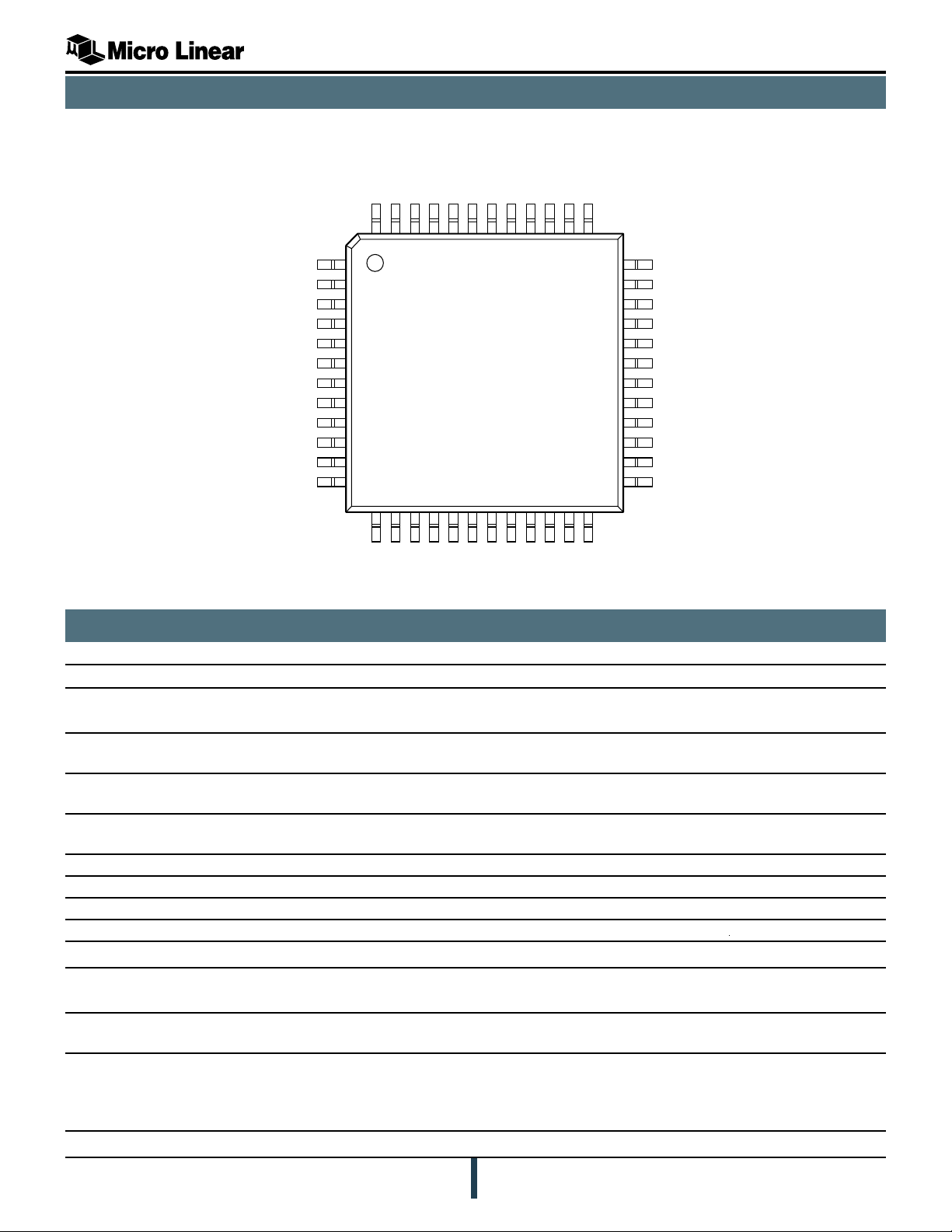
PIN CONFIGURATION
DD4
DD3
DD2
DD1
DD0
VCC1
VCC2
CMO
GND
VCC3
NC
NC
PRELIMINARY
ML2713
48-Pin TQFP (H48-7)
NC
DD5
SLICE
MS1
VDC
DFO2
DFI2
DFO1
DFI1
GND
48 47 46 45 44 43 42 41 40 39 38 37
1
2
3
4
5
6
7
8
9
10
11
12
13 14 15
18 19 20 21 22 23 24
16 17
DISCO
MS3
36
35
34
33
32
31
30
29
28
27
26
25
ML2713
NC
DPS
DPSB
VCC4
REG
MS2
BPO
BPOB
GND
1IF
1IF
VCC2
TS
RS
LOE
GND
RSSI
GND
BPI
BPIB
VCC2
2LO
LON2
VCC2
TOP VIEW
PIN DESCRIPTIONS
Pin # Signal Name I/O Type Description
POWER AND GROUND
6, 7 VCC1 POWER Voltage supply for digital I/O circuits. VCC1 should be greater than or
equal to VCC2, VCC3, and VCC4 in normal operation
21, 24, 25 VCC2 POWER Voltage supply for receive image reject down-converter and transmit
image reject up-converter
10 VCC3 POWER Voltage supply for D/A converter, comparator, mode control, and
alignment circuits
33 VCC4 POWER Voltage supply for limiters, discriminator, data filter, and transmit
regulator
9 GND GND Ground for VCC1
18, 28 GND GND Ground for VCC2
16 GND GND Ground for VCC3
39 GND GND Ground for VCC4
CONTROL
13 RS I (CMOS) Receive mode enable. This CMOS input is referenced to VCC1 and has
an on-chip pull-up. See Table 1 for operation
14 TS I (CMOS) Transmit mode enable. This CMOS input is referenced to VCC1 and has
an on-chip pull-up. See Table 1 for operation.
15 LOE I (CMOS) Chip enable and filter align control. This CMOS input is referenced to
VCC1 and has an on-chip pull up. The pin must be low for the IC to
operate in either transmit, receive or align modes. See Table 1 for
operation
4
PRELIMINARY DATASHEET
January, 2000

PRELIMINARY
ML2713
PIN DESCRIPTIONS (CONTINUED)
Pin # Signal Name I/O Type Description
CONTROL (continued)
45 MS1 MODE SELECT Auto filter alignment disable. Tie to VCC4 to disable the on-chip filter
alignment. Tie to ground for normal operation
31 MS2 MODE SELECT Receive A/D converter disable. Tie MS2 to VCC2 to disable the on-chip
comparator and D/A converter in the receive mode. The D/A will still
be enabled in the transmit mode. Tie to ground for normal operation
37 MS3 MODE SELECT Test mode control pin. Tie this pin to ground at all times
RECEIVE
8 CMO O (CMOS) Comparator output. Active in receive mode, this CMOS output that is
referenced to VCC1 and has a nominal drive capability of 10mA
17 RSSI O(ANLG) Receive Signal Strength Indicator. This output has a nominal 1Volt
range. The RSSI voltage decreases with increasing received signal
level. The RSSI output has a 10k source impedance. It is referred to
VCC2
46 SLICE I(CMOS) DC time constant restore control. This input controls whether VDC is in
the hold or acquire mode. A high on this pin puts VDC in the acquire
mode, low puts VDC in the hold mode. This CMOS input is referred to
VCC1
RECEIVE AND TRANSMIT
47 DD5 I (CMOS) Six data inputs to Digital to Analog Converter. Inputs are not latched.
DD5 is the most significant bit (MSB).
1 DD4 I (CMOS) DD4
2 DD3 I (CMOS) DD3
3 DD2 I (CMOS) DD2
4 DD1 I (CMOS) DD1
5 DD0 I (CMOS) DD0 is the least significant bit (LSB)
22 2LO
23 2LOB I(ANLG) 2LO input. These pins are connected to a differential input stage that is
connected in a common base configuration. A pull-down resistor with a
nominal value of 4k is required on each pin to bias this input. The pull
down resistors are included on the ML2712 and do not need to be added
if that chip is used. The nominal differential input impedance is 200W
26 1IF
27 1IFB I/O(ANLG) Receive 1IF input and transmit 2IF output. These pins are bi-directional
I/O are connected to the receive input amplifier and transmit output
amplifier. These pins have a nominal differential impedance of 340W
set by on-chip resistances
TRANSMIT
32 REG O (ANLG) Transmit regulator output. This output of the on-chip regulator is
enabled in transmit mode. The nominal output voltage of the regulator
is 2.8V and drives current up to 25mA. The pin requires a de-coupling
capacitor with a nominal value 100nF
FILTERS - RECEIVE
35 DPS
34 DPSB ANLG Discriminator phase shift. These pins connect to the external
discriminator phase shift filter. These pins have a nominal differential
impedance of 600W set by on-chip resistors
January, 2000
PRELIMINARY DATASHEET
5

PRELIMINARY
ML2713
PIN DESCRIPTIONS (CONTINUED)
Pin # Signal Name I/O Type Description
FILTERS - RECEIVE (continued)
38 DISCO O (ANLG) Discriminator voltage output. This emitter follower provides a nominal
drive capability of 100mA and a 200W source impedance
40 DFI1 I (ANLG) Stage 1 data filter input. Two on-chip operational amplifiers, Stage 1
and Stage 2, can be configured to make a 5th order filter with the use of
external resistors and capacitors
41 DFO1 O(ANLG) Stage 1 data filter output. The nominal output drive capability is
100mA
42 DFI2 I (ANLG) Stage 2 data filter input
43 DFO2 O (ANLG) Stage 2 data filter output. The nominal output drive capability is 100mA
44 VDC I/O (ANLG) DC time constant restore. An external capacitor sets the acquisition
time constant of the DC receiver restoration circuits that feed the on-
chip receive comparator. In the acquisition mode the nominal
impedance is 15kW. In hold mode the impedance is much higher, with
a nominal leakage current less than 2nA. The SLICE input determines if
VDC is in hold mode or in acquisition mode. This circuit ensures that
the received signal is centered on the on-chip D/A converter by
removing DC drift and transmitter and receiver frequency errors
FILTERS – TRANSMIT AND RECEIVE
19 BPI
20 BPIB I(FLTR) 2IF filter input. These pins connect to the receive image reject down-
convert mixer in the receive mode, to the 6-bit D/A converter in the
transmit mode, and to the 2LO input in the filter align mode. These
pins have a nominal differential impedance of 450 ohms set by on-chip
resistances
29 BPOB O(FLTR) 2IF filter output. These pins connect to the discriminator 0/90 phase
shift circuit in the receive mode and alignment modes, and the transmit
image reject up-convert mixer in the transmit mode
30 BPO
NON-CONNNECTED PINS
11, 12, 36, 48 NC No connect These pins should be left open
6
PRELIMINARY DATASHEET
January, 2000
 Loading...