

Micro Linear Corporation ML2350CIS-5, ML2350CCS-12, ML2350CCS-5, ML2350CIS-12, ML2350CCP-5 Datasheet
...
May 1997
ML2340*, ML2350**
Single Supply, Programmable
8-Bit D/A Converters
GENERAL DESCRIPTION
The ML2340 and ML2350 are CMOS voltage output, 8-bit
D/A converters with an internal voltage reference and a µP
interface. These devices are designed to be powered by a
single supply, although they can be powered from dual
power supplies. The output voltage swings above zero
scale (VZS) in the unipolar mode or around zero scale
(VZS) in the bipolar mode, both with programmable gain.
VZS can be set to any voltage from AGND to 2.25V below
VCC. The digital and analog grounds, DGND and AGND,
are totally independent of each other. DGND can be set to
any voltage from AGND to 4.5V below VCC for easy
interfacing to standard TTL and CMOS logic families.
The high level of integration and versatility of the ML2340
and ML2350 makes them ideal for a wide range of
applications in hard disk drives, automotive, telecom, and
a variety of general purpose industrial uses. One specific
intended application is controlling a hard disk voice coil.
The internal reference of the ML2340 provides a 2.25V or
4.50V output for use with A/D converters that use a single
5V ±10% power supply, while the ML2350 provide a
2.50V or 5.00V reference output.
FEATURES
■ Programmable output voltage gain settings of 2, 1,
1
/2, 1/4 provide 8-, 9-, 10-, or 11-bit effective resolution
around zero
■ AGND to V
■ Bipolar or unipolar output voltage
■ 4.5V to 13.2V single supply or ±2.25V to ±6.5V
dual-supply operation
■ Transparent latch allows microprocessor interface
with 30ns setup time
■ Data flow-through mode
■ Voltage reference output
ML2340 ........................................... 2.25V or 4.50V
ML2350 ........................................... 2.50V or 5.00V
■ Nonlinearity....................................±
■ Output voltage settling time over temperature and
supply voltage tolerance
Within 1V of VCC and AGND ................... 2.5µs max
Within 100mV of VCC and AGND ............... 5µs max
■ TTL and CMOS compatible digital inputs
■ Low supply current (5V supply) ..................... 5mA max
■ 18-pin DIP or surface mount SOlC
output voltage swing
CC
1
/4 LSB or ±1/2 LSB
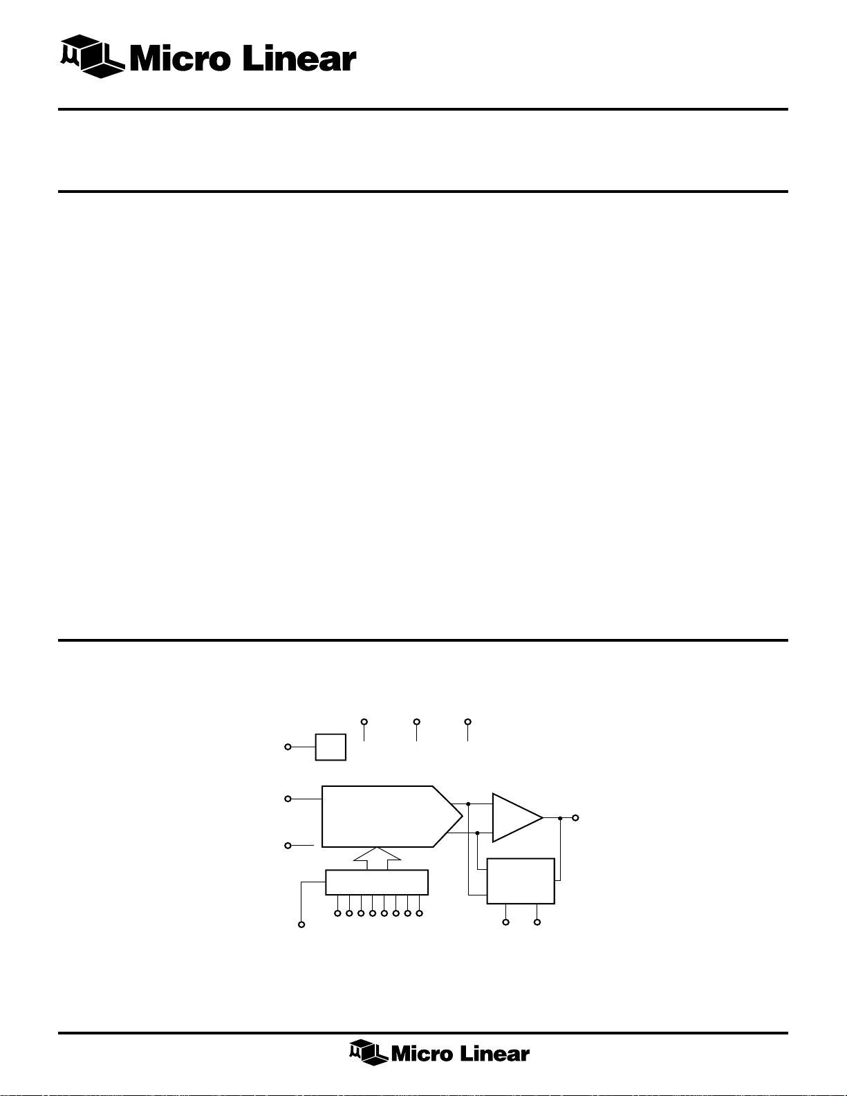
BLOCK DIAGRAM
V
REFOUT
V
DGND
REFIN
XFER
V
REF
DB0
(LSB)
V
ZS
8-BIT D/A
DATA LATCH
V
CC
DB7
(MSB)
AGND
–
OP
AMP
+
RESISTORS
SWITCHES
DECODERS
GAIN 0 GAIN 1
V
OUT
* This Part Is Obsolete
** This Part Is End Of Life As Of August 1, 2000
1
ML2340, ML2350
PIN CONNECTIONS
ML2340
ML2350
18-Pin DIP (P18)
V
1
CC
V
AGND
DGND
OUT
V
DB0
DB1
DB2
DB3
ZS
2
3
4
5
6
7
8
9
TOP VIEW
V
18
REF IN
V
17
REF OUT
GAIN 1
16
GAIN 0
15
XFER
14
DB7
13
DB6
12
DB5
11
DB4
10
V
V
OUT
AGND
DGND
DB0
DB1
DB2
DB3
ML2340
ML2350
18-Pin SOIC (S18W)
1
CC
2
3
V
ZS
4
5
6
7
8
9
TOP VIEW
PIN DESCRIPTION
PIN NAME FUNCTION PIN NAME FUNCTION
1V
CC
2V
OUT
3V
ZS
4 AGND Analog ground.
5 DGND Digital ground. This is the ground
6 DB0 Data input — Bit 0 (LSB).
7 DB1 Data input — Bit 1.
Positive supply.
Voltage output of the D/A converter.
V
is referenced to VZS.
OUT
Zero Scale Voltage. V
is referenced
OUT
to VZS. VZS is normally tied to AGND
in the unipolar mode or to mid-supply
in the bipolar mode. When the device
is operated from a single power
supply, VZS has a maximum current
requirement of –300µA in the bipolar
mode.
reference level for all digital inputs.
The range is AGND - DGND - VCC –
4.5V. DGND is normally tied to
system ground.
8 DB2 Data input — Bit 2.
9 DB3 Data input — Bit 3.
10 DB4 Data input — Bit 4.
11 DB5 Data input — Bit 5.
12 DB6 Data input — Bit 6.
13 DB7 Data input — Bit 7 (MSB).
14 XFER Transfer enable input. The data is
transferred into the transparent latch at
the high level of XFER.
15 GAIN 0 Digital gain setting input 0.
16 GAIN 1 Digital gain setting input 1.
17 V
REF OUT
Voltage reference output. V
referenced to AGND. V
to 2.5V and 5.0V in a low-voltage and
high-voltage operation, respectively
for the ML2350; 2.25V and 4.5V for
the ML2340.
18 V
REF IN
Voltage reference input. V
referenced to AGND.
18
V
REF IN
17
V
REF OUT
16
GAIN 1
15
GAIN 0
14
XFER
13
DB7
12
DB6
11
DB5
10
DB4
REF OUT
REF OUT
REF IN
is
is set
is
2
ML2340, ML2350
ABSOLUTE MAXIMUM RATINGS
Absolute maximum ratings are those values beyond which
the device could be permanently damaged. Absolute
maximum ratings are stress ratings only and functional
device operation is not implied.
Supply Voltage VCC with Respect to AGND ............ 14.2V
DGND ............................................ –0.3V to VCC + 0.3V
VZS, V
................................................–0.3V to V
REF IN
+ 0.3V
CC
OPERATING CONDITIONS
Supply Voltage, VCC.......................... 4.5VDC to 13.2V
Temperature Range
ML2350BIJ .......................................... –40°C to +85°C
ML2340BCP, ML2340CCP
ML2350BCP, ML2350CCP
ML2340BCS, ML2340CCS
ML2350BCS, ML2350CCS ..................... 0°C to +70°C
Logic Inputs .................................... –0.3V to VCC + 0.3V
Input Current per Pin ............................................ ±25mA
Storage Temperature..............................–65°C to +150°C
Package Dissipation at TA = 25°C (Board Mount) ... 875mW
Lead Temperature (Soldering 10 sec.)
Dual-In-Line Package (Molded).......................... 260°C
Dual-In-Line Package (Ceramic)......................... 300°C
Molded Small Outline IC Package
Vapor Phase (60 sec.) ..................................... 215°C
Infrared (15 sec.) ............................................ 220°C
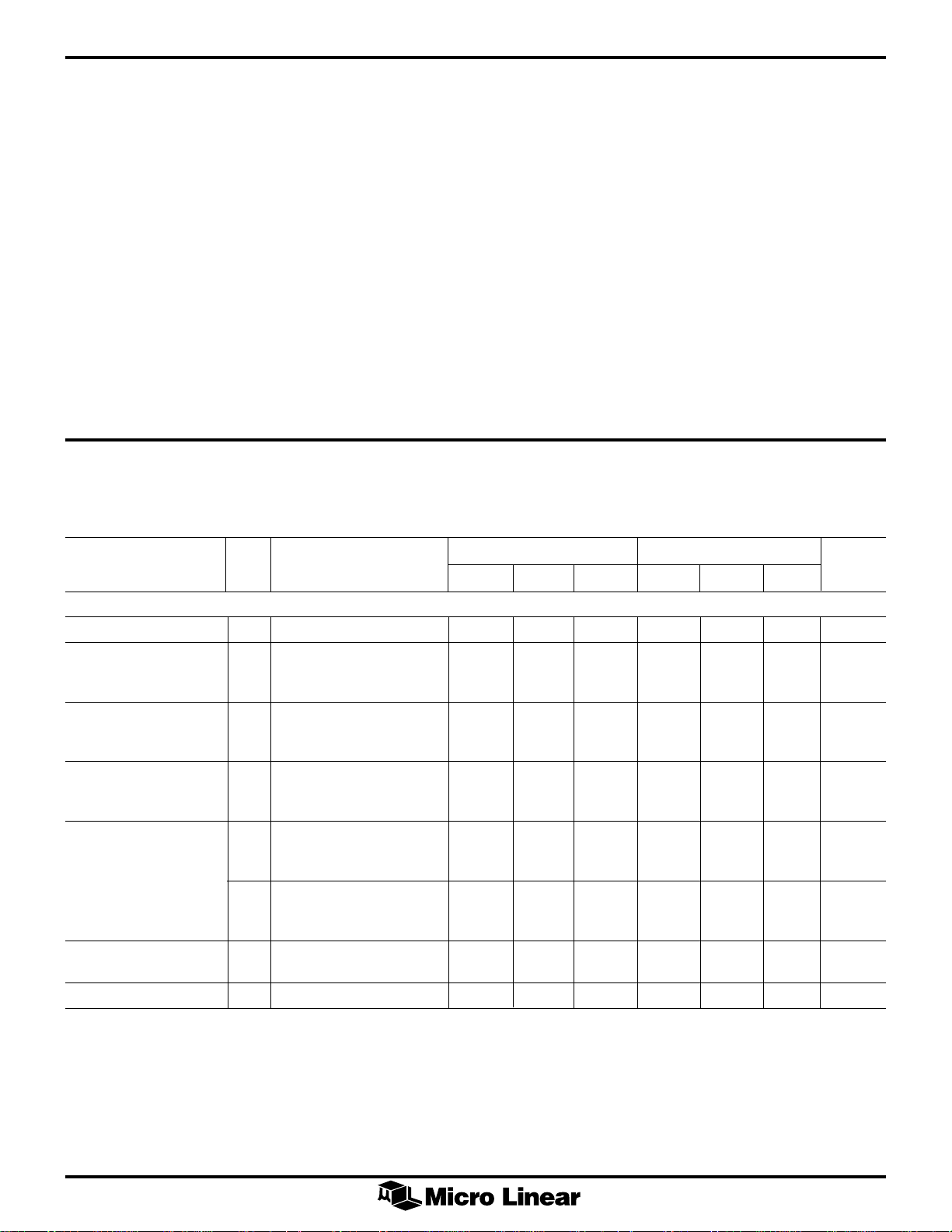
ELECTRICAL CHARACTERISTICS
Unless otherwise specified, TA = Operating temperature range, VCC – AGND = 5V ±10% and 12V ±10%, V
ML2340 = 2.25V and 4.50V, for ML2350 V
RL = 1kW and CL = 100pF and input control signals with tR = tF - 20ns. (Note 1)
= 2.50V and 5.00V, V
REF IN
load is RL = 1kW and CL = 100pF, V
OUT
ML2340XCX, ML2350XCX ML2350XIX
REF IN
for
REF
DC
load is
PARAMETER NOTES CONDITIONS MIN TYP MAX MIN TYP MAX UNITS
Converter and Programmable Gain Amplifier
Converter Resolution 8 8 Bits
Integral Linearity Error GAIN = 2, 1,
ML2340BXX, ML2350BXX ±1/4 ±1/4 LSB
ML2340CXX, ML2350CXX ±1/2 ±1/2 LSB
Differential Linearity Error GAIN = 2, 1,
ML2340BXX, ML2350BXX ±1/4 ±1/4 LSB
ML2340CXX, ML2350CXX ±1/2 ±1/2 LSB
Mode Select V
Unipolar Output 0 1.0 0 1.0 V
Bipolar Output 1.50 VCC–2.25 1.50 VCC–2.25 V
Offset Error Figure 1
Unipolar Mode GAIN = 1/4, 1/2, 1 ±10 ±12 mV
Bipolar Mode Figure 1
Gain Error Figure 1
Unipolar Mode GAIN = 1/4, 1/2, 1, 2 ±0.5 ±2 ±0.5 ±2.5 %FS
Bipolar Mode GAIN = 1/4, 1/2, 1, 2 ±0.5 ±2 ±0.5 ±2.5 %FS
with respect to AGND
ZS
GAIN = 2 ±20 ±24 mV
GAIN =
1
/2, or 1/4
1
/2, or 1/4
1
/4, 1/2, 1, 2 ±10 plus ±10 plus mV
±21/2 LSB ±21/2 LSB
3
ML2340, ML2350
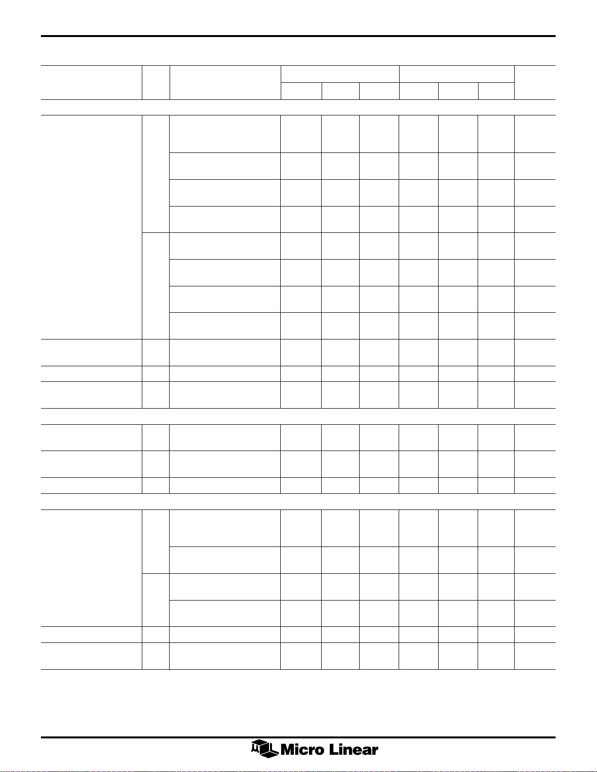
ELECTRICAL CHARACTERISTICS (Continued)
ML2340XCX, ML2350XCX ML2350XIX
PARAMETER NOTES CONDITIONS MIN TYP MAX MIN TYP MAX UNITS
Reference
V
ML2340BXX V
ML2340CXX V
ML2350BXX V
ML2350CXX V
Temperature Coefficient
V
V
V
Rejection Ratio Sinewave on V
V
V
V
Resistance
VZS Voltage Range 2 VCC - 7.0V AGND VCC–2.25 AGND VCC–2.25 V
Analog Output
V
Unipolar Mode 2 R
Bipolar Mode R
V
Power Supply 100mV
Rejection Ratio sinewave on V
Voltage
REF OUT
REF OUT
Output Current 0.75 5 0.75 5 mA
REF
Power Supply 100mV
REF OUT
and V
REF IN
REF IN
ZS
Input Range VCC - 8.75V AGND+2 VCC–1.75 AGND+2 VCC–1.75 V
- 7.0V TA = 25°C 2.23 2.25 2.27 2.23 2.25 2.27 V
CC
V
• 8.0V TA = 25°C 4.48 4.50 4.52 4.48 4.50 4.52 V
CC
- 7.0V TA = 25°C 2.22 2.25 2.29 2.22 2.25 2.28 V
CC
V
• 8.0V TA = 25°C 4.45 4.50 4.55 4.45 4.50 4.55 V
CC
- 7.0V TA = 25°C 2.48 2.50 2.52 2.48 2.50 2.52 V
CC
• 8.0V TA = 25°C 4.98 5.00 5.02 4.98 5.00 5.02 V
V
CC
- 7.0V TA = 25°C 2.45 2.50 2.55 2.46 2.50 2.55 V
CC
• 8.0V TA = 25°C 4.95 5.00 5.05 4.95 5.00 5.05 V
V
CC
T
T
T
T
T
T
T
T
MIN
MIN
MIN
MIN
MIN
MIN
MIN
MIN
to T
to T
to T
to T
to T
to T
to T
to T
MAX
MAX
MAX
MAX
MAX
MAX
MAX
MAX
2.22 2.28 2.18 2.32 V
4.46 4.54 4.43 4.57 V
2.20 2.30 2.18 2.32 V
4.40 4.60 4.35 4.65 V
2.47 2.53 2.43 2.57 V
4.96 5.04 4.90 5.10 V
2.44 2.58 2.42 2.59 V
4.90 5.10 4.85 5.15 V
50 50 ppm/°C
, 1kHz –40 –60 –40 –60 dB
P–P
CC
VCC • 8.75V AGND+2 AGND+7 AGND+2 AGND+7 V
DC Input 10 10 M ý
REF IN
Output Swing
OUT
= 100kW AGND+ VCC–0.5 AGND+ VCC–0.5 V
L
0.01 0.01
= 1kW AGND+ VCC–1.0 AGND+ VCC–1.0 V
R
L
1.0 1.0
= 100kW AGND+ VCC–0.1 AGND+ VCC–0.1 V
L
0.1 0.1
R
= 1kW AGND + VCC–1.0 AGND + VCC–1.0 V
L
1.0 1.0
Output Current AGND+1V<V
OUT
OUT<VCC
, 1kHz –60 –60 dB
P–P
CC
–1V –10 +10 –10 +10 mA
4

ML2340, ML2350
ELECTRICAL CHARACTERISTICS (Continued)
ML2340XCX, ML2350XCX ML2350XIX
PARAMETER NOTES CONDITIONS MIN TYP MAX MIN TYP MAX UNITS
Digital and DC
V
Logical “0” 0.8 0.8 V
IN(0)
Input Voltage
V
Logical “1” 2.0 2.0 V
IN(1)
Input Voltage
I
Logical “0” VIN = DGND –1 –1 µA
IN(0)
Input Current
I
Logical “1” VIN = V
IN(1)
CC
Input Current
Supply Current,
Bipolar Mode
I
, VCC Current VCC = 5V ± 10% 5.3 5.3 mA
CC
,
I
AGND
Analog Ground Current –5.0 –5.0 mA
I
, VZS Current –90 –300 –90 –300 µA
VZS
I
, VCC Current VCC = 12V ± 10% 9.3 9.3 mA
CC
,
I
AGND
Analog Ground Current –9.0 –9.0 mA
I
, VZS Current –90 –300 –90 –300 µA
VZS
Supply Current,
Unipolar Mode
, VCC Current 3 VCC = 5V ± 10% 6.0 6.0 mA
I
CC
,
I
AGND
Analog Ground Current –4.3 –4.3 mA
I
, VZS Current –1.7 –1.7 mA
VZS
I
, VCC Current VCC = 12V ±10% 11.0 11.0 mA
CC
,
I
AGND
Analog Ground Current 3 –7.3 –7.3 mA
I
, VZS Current –3.7 –3.7 mA
VZS
AC Performance
Settling Time Figure 2,
t
S1
Output Step of AGND + 1V 1.2 2.5 1.2 3.0 µs
to VCC – 1V, RL = 1kW
t
S2
Output Step of 2.5 5 2.5 6 µs
AGND + 100mV to
VCC – 100mV, RL = 100kW
t
S3
Output Step of ±1LSB 1 1 µs
tS4, Gain Change Change of Any Gain Setting 1.1 2.5 1.1 µs
t
, XFER Pulse Width Figure 3 60 60 ns
XFER
, DB0–DB7 Figure 3 40 45 ns
t
DBS
Setup Time
t
, DB0–DB7 Figure 3 0 0 ns
DBH
Hold Time
t
, Power-On 16 16 µs
RESET
Reset Time
11µA
Note 1: Limits are guaranteed by 100% testing, sampling, or correlation with worst-case test conditions.
Note 2: Supply current and analog ground current are specified with the digital inputs stable and no load on V
Note 3: In unipolar operation with V
and AGND tied together, digital codes that represent an analog value of less than 100mV from AGND should be avoided.
ZS
OUT
.
5

ML2340, ML2350
ACTUAL
GAIN ERROR
IDEAL WITH OFFSET
OFFSET
ERROR
IDEAL WITH
OFFSET
ANALOG
OUTPUT
GAIN
ERROR
ACTUAL
IDEAL
DIGITAL INPUT
OFFSET (ZERO) ERROR
DIGITAL INPUT
IDEAL
ANALOG
OUTPUT
Unipolar Mode Unipolar Mode
Figure 1. Gain and Offset Error
GAIN 0, GAIN 1
t
XFER
V
OUT
tS1, tS2, t
S4
SETTLED TO
±1/2 LSB
S3
Figure 2. Settling Time
XFER
t
WR
DB0–DB7
t
DBS
VALID DATA
t
DBH
Figure 3. Single Buffered Mode
6

1.0 FUNCTIONAL DESCRIPTION
1.1 D/A CONVERTER
ML2340, ML2350
The D/A converter is implemented using an array of equal
current sources that are decoded semi-linearly for the four
most significant bits to improve differential linearity and to
reduce output glitch around major carries. See Figure 4.
The input voltage reference of the D/A converter is the
difference between V
and AGND. This difference
REF IN
voltage is converted to a reference current using an
internal resistor to set up the appropriate current level in
4I 4I 4I 2I I I
Figure 4. D/A Converter Implementation
the D/A converter. The D/A converter output current is
then converted to a voltage output by an output buffer
and a resistive network. The matching among the
on-chip resistors preserves the gain accuracy between
these conversions.
The D/A converter can be used in a multiplying mode by
modulating the reference input within the specified
V
REF IN
range.
4-BIT
DIVIDER
V
CC
DAC
DAC
OUT
OUT
1.2 SINGLE-SUPPLY vs. DUAL-SUPPLY OPERATION
ML2340 and ML2350 can be powered from a single
supply ranging from 4.5V to 13.2V or dual supplies
ranging from ±2.25V to ±6.6V.
The internal digital and analog circuitry is powered
between VCC and AGND. The range of DGND is
AGND - DGND - VCC – 4.5V with the logic thresholds
set between 0.8V and 2.0V above DGND (standard TTL
logic level). The range of VZS is AGND - VZS - (VCC –
2.25V).
1.3 UNIPOLAR AND BIPOLAR OUTPUT
VOLTAGE SWING
ML2340 and ML2350 can operate in either unipolar or
bipolar output voltage mode. Unipolar/bipolar mode
selection is determined by comparing the zero scale
voltage (VZS) of these devices to a precise internal
reference that is referred to AGND. VZS is ideally the
voltage that will be produced at the DAC voltage output
when the digital input data is set to all “0’s” Unipolar
mode is selected when VZS is lower than 1.00 volt, and
bipolar mode is selected when VZS is greater than 1.50
volts.
1.3.1 Unipolar Output Mode
In the unipolar mode, V
swings above VZS. Ideally the
OUT
00000000 code results in an output voltage of VZS, and
the 11111111 code results in an output voltage of
VFS x 255/256, where VFS is the full-scale voltage
determined by V
and the gain setting.
REF IN
1.3.2 Bipolar Output Mode
In the bipolar mode, V
swings around VZS. The input
OUT
data is in 2’s complement binary format. Ideally, the
00000000 code results in an output voltage of VZS; the
10000000 code results in an output voltage of (VZS – VFS);
and the 01111111 results in an output voltage of (VZS +
VFS 127/128), where VFS is the full scale output voltage
determined by V
and the gain setting.
REF IN
1.4 OUTPUT BUFFER AND GAIN SETTING
The output buffer converts the D/A output current to a
voltage output using a resistive network with proper gain
setting determined by the GAIN 0 and GAIN 1 inputs.
There are four possible gain settings for unipolar output
voltage mode and bipolar output voltage mode as listed
below:
Unipolar Output Voltage Mode
Voltage Output Swing
GAIN 1 GAIN 0 GAIN Relative to V
00
01
101 V
112 V
1
/4 V
1
/2 V
REF IN
REF IN
REF IN
REF IN
ZS
¥ 1/4
¥ 1/2
¥ 1
¥ 2
7

ML2340, ML2350
Bipolar Output Voltage Mode
GAIN 1 GAIN 0 GAIN Voltage Output
00
01
101 V
112 V
1
/4 V
1
/2 V
REF IN
REF IN
REF IN
REF IN
P-P
¥ 1/8
¥ 1/4
¥ 1/2
¥ 1
The output buffer can source or sink as much as 10mA of
current with an output voltage of at least 1V from either
VCC or AGND. As the output voltage approaches VCC or
AGND the current sourcing/sinking capability of the
output buffer is reduced. The output buffer can still swing
down to within 10mV of AGND and up to within 40mV of
VCC with a 100kW load at V
to AGND in the unipolar
OUT
operation. In the bipolar operation, the output buffer
swing is limited to about 100mV from either rails.
1.5 VOLTAGE REFERENCE
A bandgap voltage reference is incorporated on the ML2340
and ML2350. Two reference voltages can be produced by
each device. An internal comparator monitors the power
supply voltage to determine the selection of the reference
voltage. A reference voltage of 2.25 volts on the ML2340
and 2.50 volts on the ML2350 is selected when the supply
voltage is less than approximately 7.50 volts. Otherwise, a
reference voltage of 4.50 volts and 5.00 volts is selected. To
prevent the comparator from oscillating between the two
selections, avoid operation with a power supply between 70
and 8.0 volts.
The bandgap reference is trimmed for zero Temperature
Coefficient (TC) at 35°C to minimize output voltage drift
over the specified operating temperature range.
The internal reference is buffered for use by the DAC and
external circuits. The reference buffer will source more
than 5mA of current and sink more than 1mA of current.
With V
connected to V
REF IN
REF OUT
, the following output
voltage ranges of the DAC are obtained:
ML2340
V
= 2.25V with V
REF
- 7.0V VCC • 8.0V
V
Gain
Setting Unipolar Bipolar Unipolar Bipolar
1
/4 0 to 0.562V –0.281V to 0 to 1.125V –0.562V to
1
/2 0 to 1.125V –0.562V to 0 to 2.250V –1.125V to
1 0 to 2.250V –1.125V to 0 to 4.500V –2.250V to
2 0 to 4.500V –2.250V to 0 to 9.000V –4.500V to
CC
+0.281V +0.562V
+0.562V +1.125V
+1.125V +2.250V
+2.250V +4.500V
= 4.5V with
REF
ML2350
V
= 2.50V with V
REF
- 7.0V VCC • 8.0V
V
Gain
Setting Unipolar Bipolar Unipolar Bipolar
1
/4 0 to 0.625V –0.3125V to 0 to 1.25V –0.625V to
1
/2 0 to 1.250V –0.6250V to 0 to 2.50V –1.250V to
1 0 to 2.500V –1.2500V to 0 to 5.00V –2.500V to
2 0 to 5.000V –2.5000V to 0 to 10.00V –5.000V to
CC
+0.3125V +0.625V
+0.6250V +1.250V
+1.2500V +2.500V
+2.5000V +5.000V
An external reference can alternatively be used on V
= 5.0V with
REF
REF IN
to set the desired full scale voltage. The linearity of the D/A
converter depends on the reference used, however. To
insure integral linearity at an 8-bit level, a reference
voltage of no less than 2V and no more than 7V (2.75V
for operation with a low-voltage power supply) should
be used.
1.6 DIGITAL INTERFACE
The digital interface of the ML2340 and ML2350 consist
of a transfer input (XFER) and eight data inputs, DB0
through DB7. The digital interface operates in one of the
two modes:
1.6.1 Single-Buffered Mode
Digital input data on DB0–DB7 is passed through an 8-bit
transparent input latch on the rising edge of XFER.
Because the outputs of the latch are connected directly to
the inputs of the internal DAC, changes on the digital data
while the XFER input is still active will cause an
immediate change in the DAC output voltage. To hold the
input data on the latch, the XFER input needs deactivated
while the data is still stable.
1.6.2 Flow-Through Mode
In the flow-through mode, the input latch is bypassed.
When XFER is set to logic “1”, a change of data inputs,
DB0–DB7, results in an immediate update of the output
voltage.
1.7 POWER-ON-RESET
The ML2340 and ML2350 have an internal power-on-
reset circuit to initialize the device when power is first
applied to the device. The power-on-reset interval of
typically 8µs begins when the supply voltage, VCC reaches
approximately 2.0V. During the power-on-reset interval,
the transparent latch is reset to all “0’s”.
8

2.0 TYPICAL APPLICATIONS
ML2340, ML2350
4.5V
µP
V
REFOUT
V
REFIN
ML2340
D/A
WITH
REFERENCE
V
OUT
0 ≤ VIN ≤ 4.5V
+V
ML2271
REF
Figure 5. Using 4.50V Reference of D/A for Reference of A/D Using Single 5V VCC ± 10%
DB7
DB0
INT
RD
V
IN
ML2261
WR
CS
CLOCK
SOURCE
OR
TIMER
V
OUT
DATA
ADDRESS
DECODE
DB7
DB0
ML2340
D/A
XFER
D7
D0
INT
DEN
HEN
TMS320
/E14
C15
PA0
PA1
PA2
ML2350
V
GAIN 0
GAIN 1
V
CC
V
OUT
V
REFIN
REFOUT
V
AGND
Figure 6. TMS320 Interface
+5V
UNIPOLAR
V
OUT
0 TO 5V
2.50V
ZS
V
, GAIN 2 V
OUT
256 CODES
Figure 7. Single 5V Supply Unipolar V
5.0V – 100mV
OUT
2.5V
256 CODES
, GAIN 1 V
OUT
1.25V
256 CODES
, GAIN 1/2 V
OUT
0.625V
GNDGNDGND
OUT
256 CODES
GND
, GAIN 1/4
9

ML2340, ML2350
TYPICAL APPLICATIONS (Continued)
ML2340
GAIN 0
GAIN 1
V
V
V
REFOUT
AGND
+12V
V
CC
4.50V
BIPOLAR
V
OUT
AROUND
4.5V
V
OUT
OUT
REFIN
V
ZS
Figure 8. Single 12V Supply, Bipolar V
256 CODES
, GAIN 2
9.0V
6.75V
256 CODES
4.5V 4.5V 4.5V 4.5V
V
OUT
, GAIN 1
V
OUT
GND + 100mV
with 11-Bits Resolution Around 4.5V
OUT
+12V
2.25V
5.625V
256 CODES
3.375V
, GAIN 1/2
+5V +12V
V
OUT
5.062V
256 CODES
3.938V
, GAIN 1/4
MICRO-
CONTROLLER
19
+5V
PWR VC
OUTPUT+
PWR GND A
R
SENSE
OUTPUT–
PWR GND B
V(RET)
I(RET) SET
11
10
13
8
12
9
7
R(RET)
4
17
18
19
XFER
DB0
DB7
GAIN 0
GAIN 1
ML2340
V
V
REF OUT
V
REF IN
V
V
OUT
AGND
DGND
CC
22
+12V
0.1µF
16
REF
0.1µF
20
1
ZS
5
6
144
153
20
CONTROL+
CONTROL–
3
DISABLE
6
GND
POWERFAIL
1
RETRACT
5
HIGH/LOW
ML4406
Figure 9. Hard Disc Drive Servo Coil Driver Providing 13-Bit Effective Resolution
1Ω
SERVO
COIL
FROM
MOTOR
WINDINGS
10

PHYSICAL DIMENSIONS inches (millimeters)
0.890 - 0.910
(22.60 - 23.12)
18
ML2340, ML2350
Package: P18
18-Pin PDIP
0.045 MIN
(1.14 MIN)
(4 PLACES)
0.170 MAX
(4.32 MAX)
0.125 MIN
(3.18 MIN)
18
PIN 1 ID
1
0.449 - 0.463
(11.40 - 11.76)
0.050 - 0.065
(1.27 - 1.65)
0.016 - 0.022
(0.40 - 0.56)
0.100 BSC
(2.54 BSC)
SEATING PLANE
Package: S18
18-Pin SOIC
0.240 - 0.260
(6.09 - 6.61)
0.015 MIN
(0.38 MIN)
0.295 - 0.325
(7.49 - 8.26)
0º - 15º
0.008 - 0.012
(0.20 - 0.31)
0.024 - 0.034
(0.61 - 0.86)
(4 PLACES)
0.090 - 0.094
(2.28 - 2.39)
0.291 - 0.301
(7.39 - 7.65)
PIN 1 ID
1
0.050 BSC
(1.27 BSC)
0.012 - 0.020
(0.30 - 0.51)
0.095 - 0.107
(2.41 - 2.72)
SEATING PLANE
0.398 - 0.412
(10.11 - 10.47)
0.005 - 0.013
(0.13 - 0.33)
0º - 8º
0.022 - 0.042
(0.56 - 1.07)
0.009 - 0.013
(0.22 - 0.33)
11
ML2340, ML2350
ORDERING INFORMATION
INTEGRAL & DIFFERENTIAL TEMPERATURE
PART NUMBER NON-LINEARITY RANGE PACKAGE
V
= 2.25V with VCC = 5V
REF OUT
ML2340CCP/5 (OBS) ±1/2 LSB 0°C to 70°C Molded DIP (P18)
ML2340CCS/5 (OBS) 0°C to 70°C Molded SOIC (S18)
V
= 2.50V with VCC = 5V
REF OUT
ML2350CCP/5 (OBS) ±1/2 LSB 0°C to 70°C Molded DIP (P18)
ML2350CCS/5 (EOL) 0°C to 70°C Molded SOIC (S18)
ML2350CIS/5 (EOL) –40°C to 85°C Molded SOIC (S18)
V
= 4.50V with VCC = 12V
REF OUT
ML2340CCP/12 (OBS) ±1/2 LSB 0°C to 70°C Molded DIP (P18)
ML2340CCS/12 (OBS) 0°C to 70°C Molded SOIC (S18)
V
= 5.00V with VCC = 12V
REF OUT
ML2350CCP/12 (OBS) ±1/2 LSB 0°C to 70°C Molded DIP (P18)
ML2350CCS/12 (OBS) 0°C to 70°C Molded SOIC (S18)
ML2350CIS/12 (OBS) –40°C to 85°C Molded SOIC (S18)
© Micro Linear 1997 is a registered trademark of Micro Linear Corporation
Products described in this document may be covered by one or more of the following patents, U.S.: 4,897,611; 4,964,026; 5,027,116; 5,281,862; 5,283,483; 5,418,502; 5,508,570; 5,510,727; 5,523,940;
5,546,017; 5,559,470; 5,565,761; 5,592,128; 5,594,376; Japan: 2598946; 2619299. Other patents are pending.
Micro Linear reserves the right to make changes to any product herein to improve reliability, function or design.
Micro Linear does not assume any liability arising out of the application or use of any product described herein,
neither does it convey any license under its patent right nor the rights of others. The circuits contained in this
data sheet are offered as possible applications only. Micro Linear makes no warranties or representations as to
whether the illustrated circuits infringe any intellectual property rights of others, and will accept no responsibility
or liability for use of any application herein. The customer is urged to consult with appropriate legal counsel
before deciding on a particular application.
12
2092 Concourse Drive
San Jose, CA 95131
Tel: 408/433-5200
Fax: 408/432-0295
DS2340_50-01
 Loading...