

Micro Linear Corporation ML2288BCQ, ML2284CCP, ML2284CCS, ML2284CIP, ML2288BCP Datasheet
...
May 1997
ML2281, ML2282*,
ML2284#, ML2288#
Serial I/O 8-Bit A/D Converters with
Multiplexer Options
GENERAL DESCRIPTION
The ML2281 family are 8-bit successive approximation
A/D converters with serial I/O and configurable input
multiplexers with up to 8 input channels.
All errors of the sample-and-hold, incorporated on the
ML2281 family are accounted for in the analog-to-digital
converters accuracy specification.
The voltage reference can be externally set to any value
between GND and VCC, thus allowing a full conversion
over a relatively small voltage span if desired.
The ML2281 family is an enhanced double polysilicon
CMOS pin compatible second source for the ADC0831,
ADC0832, ADC0834, and ADC0838 A/D converters. The
ML2281 series enhancements are faster conversion time,
true sample-and-hold function, superior power supply
rejection, improved AC common mode rejection, faster
digital timing, and lower power dissipation. All parameters
are guaranteed over temperature with a power supply
voltage of 5V ±10%.
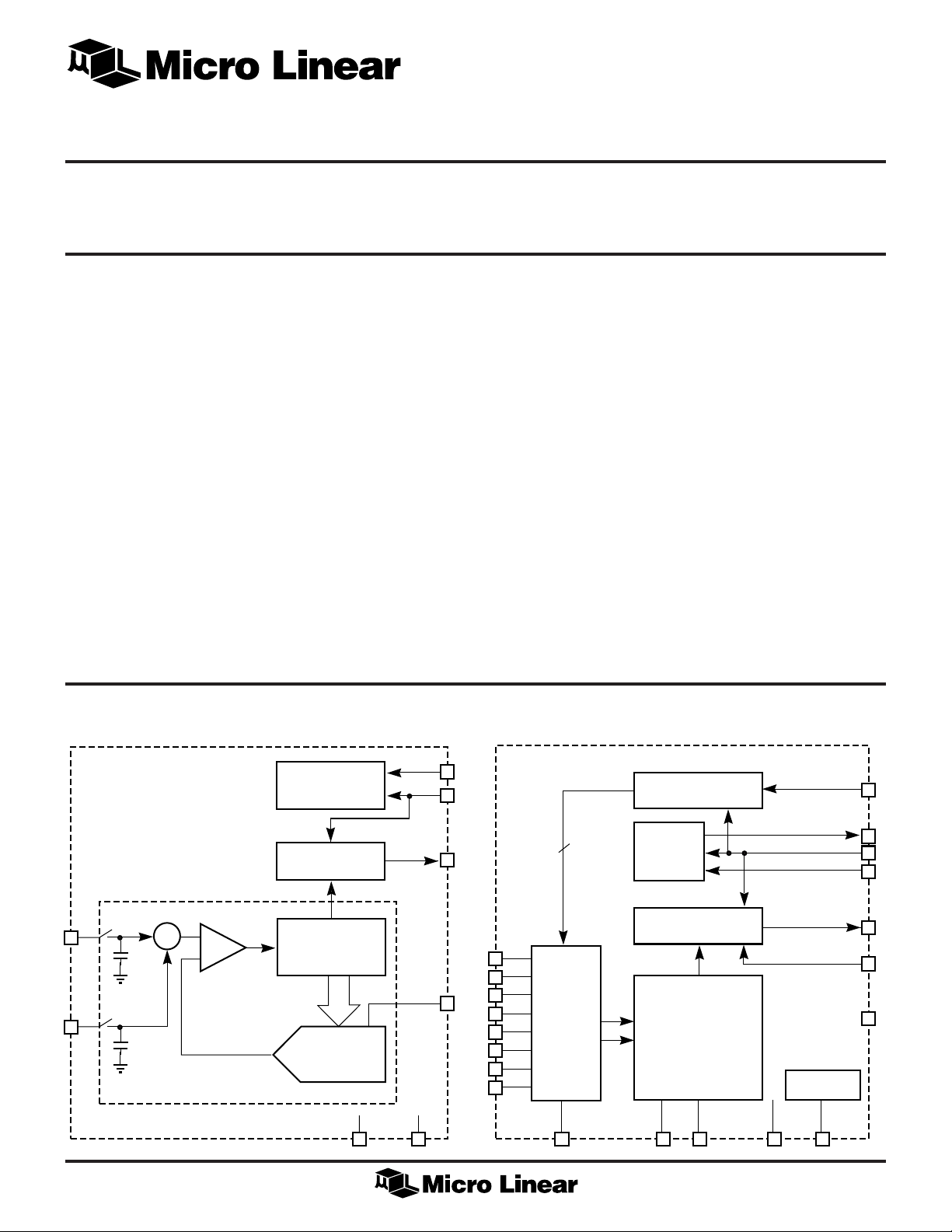
BLOCK DIAGRAM
ML2281
FEATURES
■ Conversion time: 6µs
■ Total unadjusted error: ±1/2LSB or ±1LSB
■ Sample-and-hold: 375ns acquisition
■ 2, 4 or 8-input multiplexer options
■ 0 to 5V analog input range with single 5V
power supply
■ Operates ratiometrically or with up to 5V
voltage reference
■ No zero or full-scale adjust required
■ ML2281 capable of digitizing a 5V, 40kHz sine wave
■ Low power: 12.5mW MAX
■ Superior pin compatible replacement for ADC0831,
ADC0832, ADC0834, and ADC0838
■ Analog input protection: 25mA (min) per input
■ Now in 8-Pin SOIC Package (ML2281, ML2282)
(* Indicates Part is Obsolete)
(# Indicates Part is End Of Life as Of July 1, 2000)
ML2288
ML2284
ML2284
(8-Channel SE or 4-Channel Diff Multiplexer)
(4-Channel SE or 2-Channel Diff Multiplexer)
(2-Channel SE or 1-Channel Diff Multiplexer)
A/D WITH SAMPLE & HOLD FUNCTION
V
IN+
V
IN–
8pF
8pF
+
+
Σ
COMP
–
–
CONTROL
AND
TIMING
OUTPUT
SHIFT-REGISTER
SUCCESSIVE
APPROXIMATION
REGISTER
D/A
CONVERTER
V
CC
GND
CLK
V
CS
DO
REF
CH0
CH1
CH2
CH3
CH4
CH5
CH6
CH7
COMMON
4-BIT
MULTIPLEXER
(ML2288 SHOWN)
AGND
INPUT
SHIFT-REGISTER
CONTROL
AND
TIMING
OUTPUT
SHIFT-REGISTER
A/D
CONVERTER
WITH
SAMPLE & HOLD
FUNCTION
V
REF
V
CC
DI
SARS
CLK
CS
DO
SE
DGND
SHUNT
REGULATOR
V+
1
ML2281, ML2282, ML2284, ML2288
CH0
CH1
CH2
CH3
CH4
CH5
CH6
CH7
COM
DGND
V
CC
V+
CS
DI
CLK
SARS
DO
SE
V
REF
AGND
1
2
3
4
5
6
7
8
9
10
20
19
18
17
16
15
14
13
12
11
TOP VIEW
PIN CONFIGURATION
ML2281
Single Differential Input
8-Pin DIP
CS
V
IN+
V
IN–
GND
1
2
3
4
TOP VIEW
8
7
6
5
ML2281
8-Pin SOIC
V
IN+
V
IN–
GND
CS
1
2
3
4
TOP VIEW
8
7
6
5
ML2284
14-Pin SOIC
V
CLK
DO
V
CC
REF
V
CLK
DO
V
CC
REF
2-Channel MUX
CS
CH0
CH1
GND
CS
CH0
CH1
GND
4-Channel MUX
ML2282
8-Pin DIP
1
2
3
4
TOP VIEW
ML2282
8-Pin SOIC
1
2
3
4
TOP VIEW
ML2284
14-Pin DIP
V
8
CLK
7
DO
6
DI
5
8
7
6
5
CC (VREF
VCC (V
CLK
DO
DI
REF
)
)
2
V+
CS
CH0
CH1
CH2
CH3
DGND
1
2
3
4
5
6
7
TOP VIEW
14
13
12
11
10
V
CC
DI
CLK
SARS
DO
V
9
8
REF
AGND
V+
CS
CH0
CH1
CH2
CH3
DGND
1
2
3
4
5
6
7
14
13
12
11
10
V
CC
DI
CLK
SARS
DO
V
9
REF
AGND
8
TOP VIEW
ML2288
8-Channel MUX
20-Pin PCC
ML2288
8-Channel MUX
20-Pin DIP
CH2
CH1
CH0
VCCV+
CH3
CH4
CH5
CH6
CH7
3212019
4
5
6
7
8
910111213
COM
TOP VIEW
DGND
AGND
V
REF
18
CS
17
DI
16
CLK
15
SARS
14
DO
SE

PIN DESCRIPTION
ML2281, ML2282, ML2284, ML2288
NAME FUNCTION
V
CC
DGND Digital ground. 0 volts. All digital inputs and
AGND Analog ground. The negative reference voltage
CH0-7, Analog inputs. Digitally selected to be single
VIN+, VIN– ended (VIN) or; VIN+ or VIN– of a differential
COM Common reference point for analog inputs.
V
REF
SE Shift enable. Input controls whether LSB first
V+ Input to the Shunt Regulator.
Positive supply. 5V ± 10%
outputs are referenced to this point.
for A/D converter.
input. Analog range = GND - VIN - VCC.
A/D conversion is performed on voltage
difference between analog input and this
common reference point if single-end
conversion is specified.
Reference. The positive reference voltage for
A/D converter.
bit stream is shifted out on serial output DO.
If SE = 1, MSB first is shifted out only. If SE = 0,
an MSB first bit stream is shifted out, then a
second bit stream with LSB first is shifted out
after end of conversion.
NAME FUNCTION
DO Data out. Digital output which contains result
of A/D conversion. The serial data is clocked
out on falling edges of CLK.
SARS Successive approximation register status.
Digital output which indicates that a
conversion is in progress. When SARS goes
to 1, the sampling window is closed and
conversion begins. When SARS goes to 0,
conversion is completed. When CS = 1, SARS
is in high impedance state.
CLK Clock. Digital input which clocks data in on
DI on rising edges and out on DO on falling
edges. Also used to generate clocks for A/D
conversion.
DI Data input. Digital input which contains serial
data to program the MUX and channel
assignments.
CS Chip select. Selects the chip for multiplexer
and channel assignment and A/D conversion.
When CS = 1, all digital outputs are in high
impedance state. When CS = 0, normal A./D
conversion takes place.
3
ML2281, ML2282, ML2284, ML2288
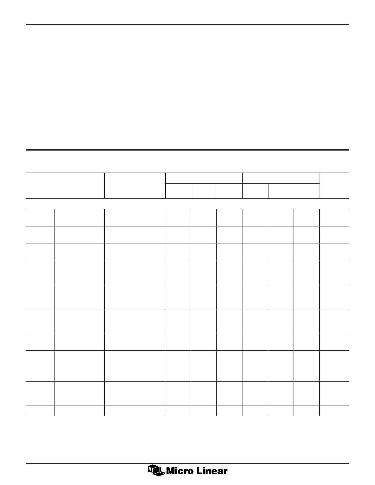
ABSOLUTE MAXIMUM RATINGS
Absolute maximum ratings are those values beyond which
the device could be permanently damaged. Absolute
maximum ratings are stress ratings only and functional
device operation is not implied.
Current into V+ ...................................................... 15mA
Supply Voltage, VCC................................................. 6.5V
Voltage
Logic Inputs ........................................... –7 to VCC +7V
Analog Inputs ................................ –0.3V to VCC +0.3V
Input Current per Pin (Note 1) .............................. ±25mA
Storage Temperature ................................ –65°C to 150°C
Package Dissipation
at TA = 25°C (Board Mount) .............................800mW
ELECTRICAL CHARACTERISTICS
Unless otherwise specified, TA = T
SYMBOL PARAMETER CONDITIONS MIN NOTE 3 MAX MIN NOTE 3 MAX UNITS
MIN
to T
MAX
, VCC = V
REF
Lead Temperature (Soldering 10 sec.)
Dual-In-Line Package (Molded) .......................... 260°C
Dual-In-Line Package (Ceramic) ......................... 300°C
Molded Chip Carrier Package
Vapor Phase (60 sec.) ..................................... 215°C
Infrared (15 sec.)............................................. 220°C
OPERATING CONDITIONS
Supply Voltage, VCC............................ 4.5VDC to 6.3V
Temperature Range (Note 2) ................. T
ML2281/2/4/8 BIX .................................. –40°C to 85°C
ML2281/2/4/8 CIX
ML2281/2/4/8 BCX ....................................0°C to 70°C
ML2281/2/4/8 CCX
= 5V ±10%, and f
ML228XB ML228XC
TYP TYP
= 1.333MHz.
CLK
MIN
- TA - T
DC
MAX
CONVERTER AND MULTIPLEXER CHARACTERISTICS
Total Unadjusted V
Error
Reference Input (Notes 4, 7) 10 15 20 10 15 20 kW
Resistance
Common-Mode (Notes 4, 8) GND V
Input Range –0.05 +0.05 –0.05 +0.05
DC Common-Mode Common mode voltage ±1/16 ±1/4 ±1/16 ±1/4 LSB
Error voltage GND to V
AC Common-Mode Common mode voltage ±1/4 ±1/4 LSB
Error GND to V
DC Power Supply VCC = 5V ±10% ±1/32 ±1/4 ±1/32 ±1/4 LSB
Sensitivity V
AC Power Supply 100mV
Sensitivity on V
Change in Zero 15mA into V+ ±1/2 ±1/2 LSB
Error from V
to Internal Zener (Note 5)
Operation
=5V VCC = N.C. V
CC
= VCC (Notes 4, 6) ±1/2 ±1 LSB
REF
,
REF
CC/2
= 5V
(Note 5)
0 to 50kHz (Note 5)
REF
(Note 5)
CC/2
- VCC +0.1V
, 25kHz sine ±1/4 ±1/4 LSB
P-P
(Note 5)
CC
CC
GND V
CC
V
V
V+ Input Resistance (Note 4) 20 35 20 35 kW
Internal Diode 15mA into V+ 6.9 6.9 V
Z
Regulated Breakdown (at V+)
4

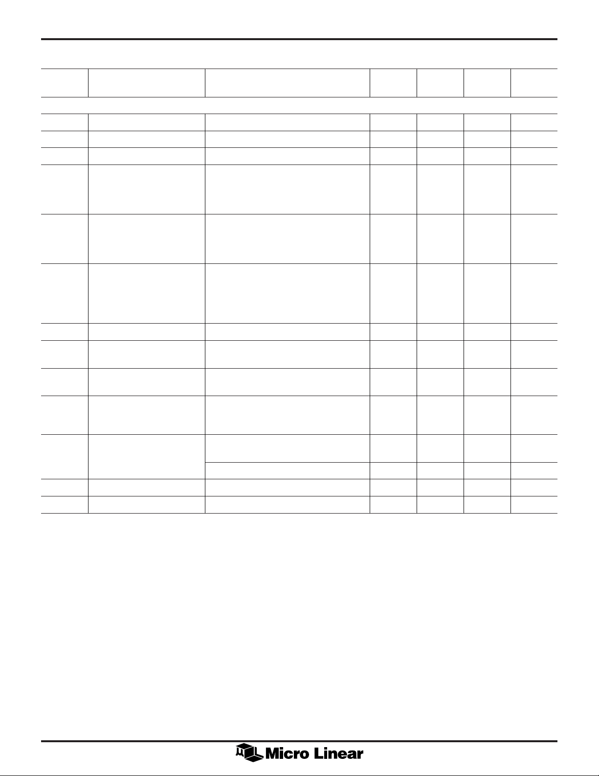
ML2281, ML2282, ML2284, ML2288
ELECTRICAL CHARACTERISTICS
(Continued)
ML228XB ML228XC
TYP TYP
SYMBOL PARAMETER CONDITIONS MIN NOTE 3 MAX MIN NOTE 3 MAX UNITS
CONVERTER AND MULTIPLEXER CHARACTERISTICS (CONTINUED)
I
OFF
Off Channel On channel = V
CC
–1 –1 µA
Leakage Current Off channel = 0V
(Notes 4, 9)
On channel = 0V +1 +1 µA
Off channel = V
CC
(Notes 4, 9)
I
ON
On Channel On channel = 0V –1 –1 µA
Leakage Current Off channel = V
CC
(Notes 4, 9)
On channel = V
CC
+1 +1 µA
Off channel = 0V
(Notes 4, 9)
DIGITAL AND DC CHARACTERISTICS
V
IN(1)
Logical “1” (Note 4) 2.0 2.0 V
Input Voltage
V
IN(0)
Logical “0” (Note 4) 0.8 0.8 V
Input Voltage
I
IN(1)
Logical “1” Input VIN = V
Current
I
IN(0)
Logical “0” Input VIN = 0V (Note 4) –1 –1 µA
Current
V
OUT(1)
Logical “1” I
Output Voltage
V
OUT(0)
Logical “0” I
Output Voltage
I
OUT
HI-Z Output V
Current V
I
SOURCE
Output Source V
Current
I
SINK
I
CC
Output Sink Current V
Supply Current ML2281, ML2284 1.3 2.5 1.3 2.5 mA
(Note 4) 1 1 µA
CC
= –2mA (Note 4) 4.0 4.0 V
OUT
= 2mA (Note 4) 0.4 0.4 V
OUT
= 0V (Note 4) –1 –1 µA
OUT
= V
OUT
OUT
OUT
CC
= 0V (Note 4) –6.5 –6.5 mA
= V
(Note 4) 8.0 8.0 mA
CC
11µA
ML2288 (Note 4)
ML2282 Includes ladder 1.8 3.5 1.8 3.5 mA
Current (Note 4)
5
ML2281, ML2282, ML2284, ML2288
ELECTRICAL CHARACTERISTICS
(Continued)
TYP LIMIT
SYMBOL PARAMETER CONDITIONS MIN NOTE 3 MAX UNITS
AC ELECTRICAL CHARACTERISTICS
f
CLK
t
ACQ
t
C
SNR Signal to Noise Ratio VIN = 40kHz, 5V sine. f
Clock Frequency (Note 4) 10 1.333 kHz
Sample-and-Hold Acquisition 1/2 1/f
Conversion Time Not including MUX adddressing time 8 1/f
= 1.333MHz 47 dB
ML2281 (f
SAMPLING
» 120kHz). Noise is sum of all
CLK
nonfundamental components up to 1/2
of f
SAMPLING
THD Total Harmonic Distortion VIN = 40kHz, 5V sine. f
ML2281 (f
SAMPLING
(Note 11)
= 1.333MHz –60 dB
CLK
» 120kHz). THD is sum of 2,
3, 4, 5 harmonics relative to fundamental
(Note 11)
IMD Intermodulation Distortion V
ML2281 f
= fA + fB. fA = 40kHz, 2.5V sine. –60 dB
IN
= 39.8kHz, 2.5V Sine, f
B
(f
SAMPLING
– fB), (2fA + fB), (2fA – fB), (fA + 2fB),
(f
A
» 120kHz). IMD is (fA + fB),
= 1.333MHz
CLK
(fA – 2fB) relative to fundamental (Note 11)
Clock Duty Cycle (Notes 4, 10) 40 60 %
CLK
CLK
t
SET-UP
CS Falling Edge or Data Input (Note 4) 130 ns
Valid to CLK Rising Edge
t
HOLD
Data Input Valid after (Note 4) 80 ns
CLK Rising Edge
t
, CLK Falling Edge to Output CL = 100pF (Note 4 & 12)
PD1
t
PD0
Data Valid Data MSB first 90 200 ns
Data LSB first 50 110 ns
t
, Rising Edge of CS to Data CL = 10pF, RL = 10k (see high impedance 40 90 ns
1H
t
0H
Output and SARS Hi-Z test circuits) (Note 5)
CL = 100pF, RL = 2k (Note 4) 80 160 ns
C
IN
C
OUT
Note 1: When the input voltage (VIN) at any pin exceeds the power supply rails (VIN < GND or VIN > VCC) the absolute value of current at that pin should be limited to 25mA
Note 2: 0°C to 70°C and –40°C to +85°C operating temperature range devices are 100% tested with temperature limits guaranteed by 100% testing, sampling, or by
Note 3: Typicals are parametric norm at 25°C.
Note 4: Parameter guaranteed and 100% production tested.
Note 5: Parameter guaranteed. Parameters not 100% tested are not in outgoing quality level calculation.
Note 6: Total unadjusted error includes offset, full-scale, linearity, multiplexer and sample-and-hold errors.
Note 7: Cannot be tested for ML2282.
Note 8: For V
Note 9: Leakage current is measured with the clock not switching.
Note 10: A 40% to 60% clock duty cycle range insures proper operation at all clock frequencies. In the case that an available clock has a duty cycle outside of these limits, the
Note 11: Because of multiplexer addressing, test conditions for the ML2282 would be V
Note 12: Since data, MSB first, is the output of the comparator used in the successive approximation loop, an additional delay is built in (see Block Diagram) to allow for
Capacitance of Logic Input 5 pF
Capacitance of Logic Outputs 5 pF
or less.
correlation with worst-case test conditions.
– ³ VIN+ the digital output code will be 0000 0000. Two on-chip diodes are tied to each analog input (see Block Diagram) which will forward conduct for
IN
analog input voltages one diode drop below ground or one diode drop greater than the V
analog inputs (5V) can cause this input diode to conduct—especially at elevated temperatures, and cause errors for analog inputs near full-scale. The spec allows
50mV forward bias of either diode. This means that as long as the analog V
correct. To achieve an absolute 0V to 5V input voltage range will therefore require a minimum supply voltage of 4.950V
tolerance and loading.
minimum time the clock is high or the minimum time the clock is low must be at least 300ns. The maximum time the clock can be high or low is 60µs.
(f
comparator response time.
» 95kHz); ML2288 VIN = 30kHz, 5V sine (f
SAMPLING
SAMPLING
» 89kHz).
or V
IN
= 34kHz, 5V sine (f
IN
supply. Be careful, during testing at low VCC levels (4.5V), as high level
CC
does not exceed the supply voltage by more than 50mV, the output code will be
REF
» 102kHz); ML2284 VIN = 32kHz, 5V sine
SAMPLING
over temperature variations, initial
DC
6
ML2281, ML2282, ML2284, ML2288
DATA
OUTPUT
DATA
OUTPUT
t
1H
V
CC
CS
R
C
L
L
DO AND
SARS OUTPUTS
t
0H
V
CC
R
L
C
L
DO AND
SARS OUTPUTS
CS
GND
V
OH
GND
V
GND
V
V
t
1H
t
r
90%
50%
10%
t
1H
90%
t
0H
t
50%
10%
t
r
90%
0H
10%
CC
CC
OL
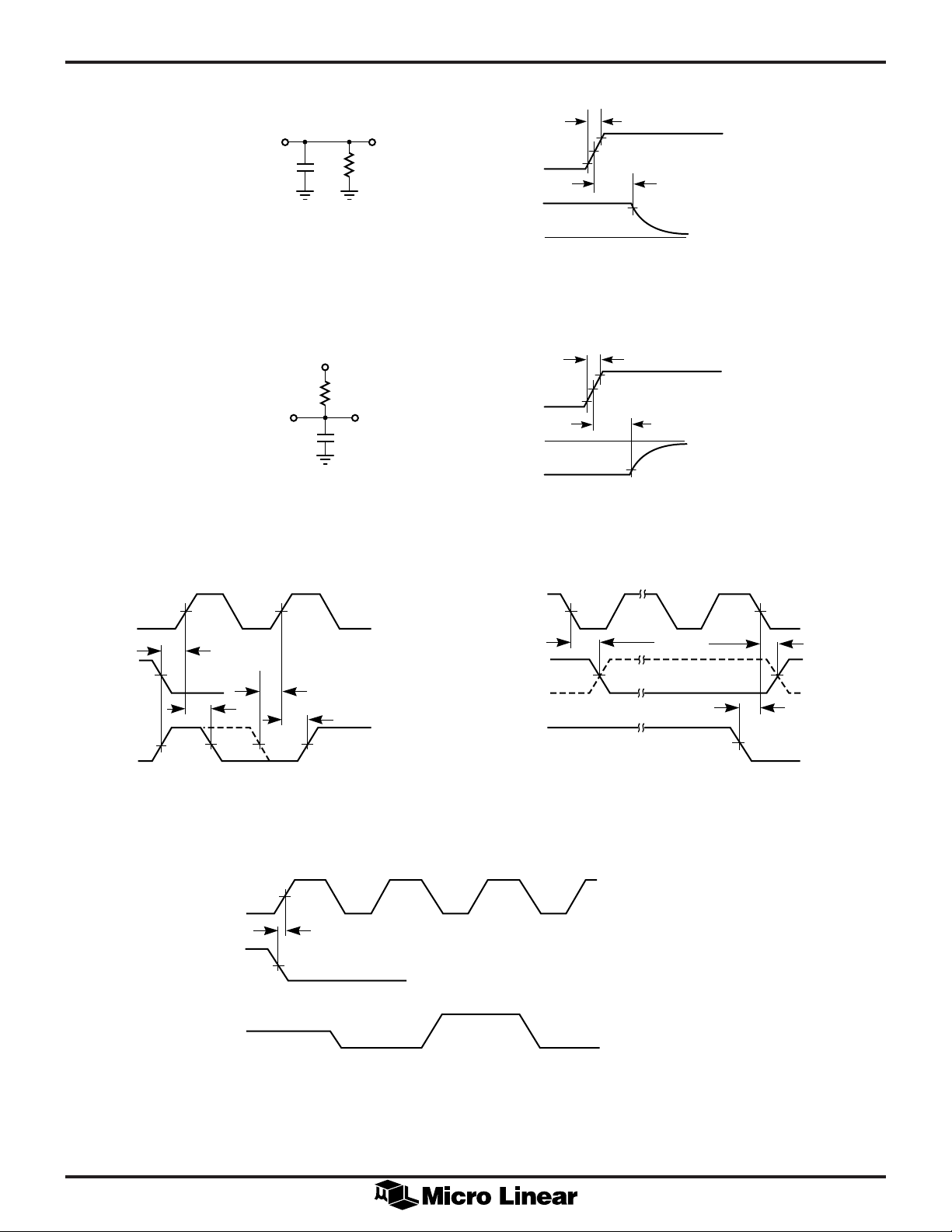
Figure 1. High Impedance Test Circuits and Waveforms
CLK
CS
DATA
IN (DI)
Data Input Timing
t
SET-UP
t
HOLD
CLK
CS
t
SET-UP
t
HOLD
ML2281 Start Conversion Timing
t
SET-UP
START CONVERSION
CLK
DATA
OUT (DO)
Data Output Timing
t
PD0, tPD1
SE
t
SET-UP
t
PD0, tPD1
DO
BIT 7
(MSB)
Figure 2. Timing Diagrams
BIT 6
7
ML2281, ML2282, ML2284, ML2288
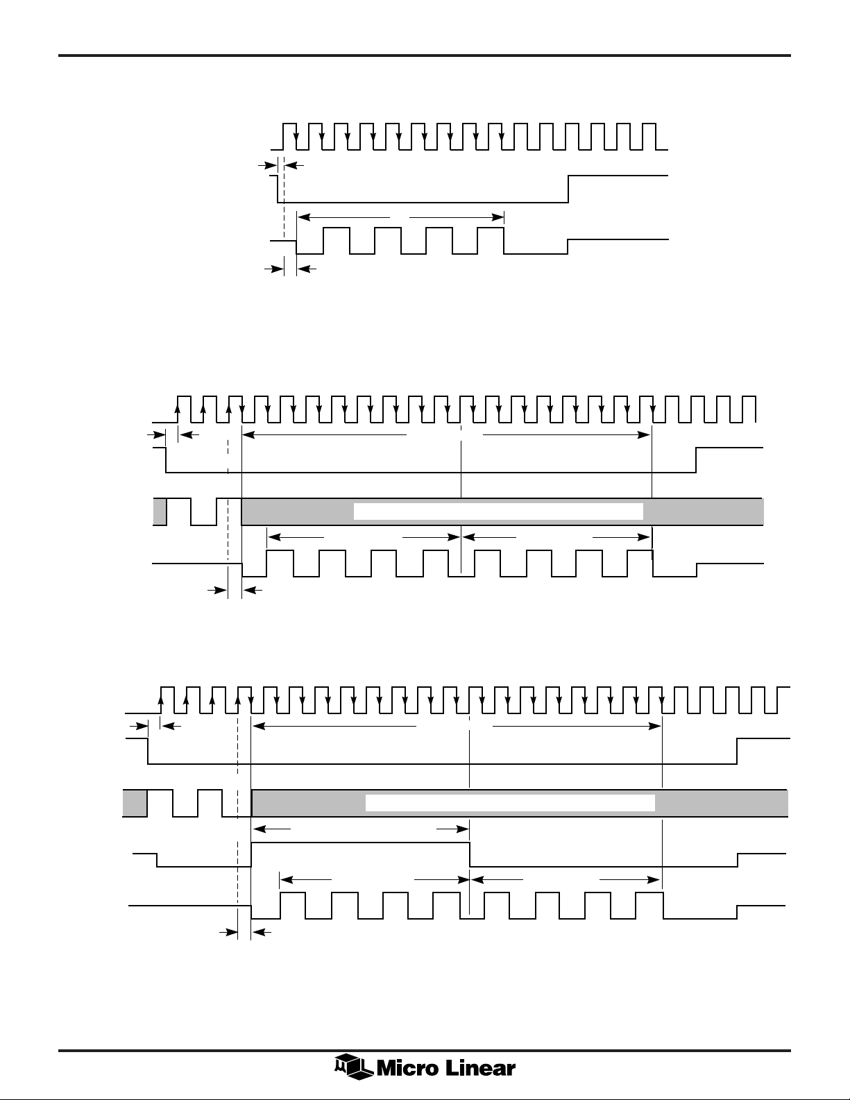
ML2281 Timing
1
234567891011
CLOCK (CLK)
t
SET-UP
CHIP SELECT (CS)
t
C
DATA OUT (DO)
SAMPLE & HOLD
ACQUISITION (t
1234567891011121314151617181920
CLOCK (CLK)
ACQ
HI-Z
)
76 543210
(MSB)
*LSB FIRST OUTPUT NOT AVAILABLE ON ML2281
ML2282 Timing
(LSB)
*
HI-Z
CHIP SELECT (CS)
DATA IN (DI)
DATA OUT (DO)
ACQUISITION (t
CLOCK (CLK)
CHIP SELECT (CS)
DATA IN (DI)
SAR STATUS (SARS)
ADDRESS MUX
START
BIT
SGL/DIF
HI-Z HI-Z
SAMPLE & HOLD
ACQ
t
SET-UP
)
ODD/
SIGN
DON’T CARE (DI DISABLED UNTIL NEXT CONVERSION CYCLE)
7654 321 123456
(MSB)
OUTPUT DATA
0
(LSB)
LSB FIRST DATAMSB FIRST DATA
7
(MSB)
ML2284 Timing
1234567891011121314151617181920
t
SET-UP
ADDRESS MUX
START
ODD/SIGN
BIT
DON’T CARE (DI DISABLED UNTIL NEXT CONVERSION CYCLE)
SGL/DIF SELECT
BIT 1
HI-Z HI-Z
A/D CONVERSION IN PROCESS
OUTPUT DATA
LSB FIRST DATAMSB FIRST DATA
DATA OUT (DO)
8
HI-Z HI-Z
SAMPLE & HOLD
ACQUISITION (t
ACQ
765432 012345
)
(MSB)
1
(LSB)
67
(MSB)
Figure 2. Timing Diagrams (Continued)

CLOCK (CLK)
ML2281, ML2282, ML2284, ML2288
ML2288 Timing
1234567891011121314151617181920212223242526
CHIP SELECT (CS)
DATA IN (DI)
SAR STATUS (SARS)
SE = “0”
DATA OUT (DO)
USING SE
TO CONTROL
LSB FIRST
OUTPUT
DO
START
SE
SAMPLE & HOLD
ACQUISITION (t
t
SET-UP
ADDRESS MUX
ODD/
SIGN
ACQ
SELECT
BIT 0
SELECT
BIT 1
)
DON’T CARE (DI DISABLED UNTIL NEXT CONVERSION CYCLE)
A/D CONVERSION IN PROCESS
765432 01234 5
(MSB)
7654321 0 1234567
BIT
SGL/DIF
HI-Z HI-Z
1
(LSB)
OUTPUT DATA
LSB FIRST DATAMSB FIRST DATA
DATA HELD LSB FIRST DATAMSB FIRST DATA
(LSB) (MSB)(MSB)
t
SET-UP
67
(MSB)
Figure 2. Timing Diagrams (Continued)
HI-ZHI-Z
HI-ZHI-Z
1.0
0.75
0.5
–55 C
LINEARITY ERROR (LSB)
0.25
25 C
0
0 0.01 0.1 1
CLOCK FREQUENCY (MHz)
125 C
Figure 3. Linearity Error vs f
VCC = 5V
V
= 5V
REF
CLK
9

ML2281, ML2282, ML2284, ML2288
1
V
= 5V
CC
f
= 1.333MHz
CLK
0.75
0.5
–55 C
LINEARITY ERROR (LSB)
0.25
0
0235
Figure 4. Linearity Error vs V
125 C
25 C
41
V
(VDC)
REF
Voltage
REF
1
0.75
0.5
OFFSET ERROR (LSB)
0.25
0
0235
V
REF
V
= 5V
CC
V
= 0V
IN
f
= 1.333MHz
CLK
T
= 25 C
A
(VDC)
Figure 5. Unadjusted Offset Error vs V
41
REF
Voltage
10

DI*
CS
ML2281, ML2282, ML2284, ML2288
17
18
CLK
CH0*
CH1*
CH2
CH3
CH4*
CH5*
CH6*
CH7*
COM*
V
REF
V
CC
V+*
DGND*
AGND*
RRRR R
16
V
CC
1
2
3
4
5
6
7
8
9
12
20
INPUT PROTECTION—ALL LOGIC INPUTS
5-BIT SHIFT-REGISTER
SGL/DIF
7V SHUNT
REGULATOR
ODD/
SIGN
MUX
ADDRESS
TO INTERNAL
CIRCUITRY
INPUT
13
16
17
18
NOTE 1
ANALOG
(EQUIVALENT)
V
CC
TO
INTERNAL
CIRCUITS
+
MUX
SELECT 0SELECT 1START
Σ
–
R
NOTE 1
C
C
LADDER
AND
DECODER
D
C
+
–
COMP
COMP
SAR
LOGIC
AND
LATCH
T
D
TIME
DELAY
DSTART 2
CS
B7
B6
B5
B4
B3
B2
B1
B0
LSB FIRST
CS
START
RRC
9-BIT
SHIFT
REGISTER
EOC
CS
EOC
13
CQR
DCQ
DCQ
C
R
D
D
R
R
Q
SE*
CS
DEOC
SARS*
15
CS
CS
CS
DSTART 1
CS
14
DO
MSB FIRST
PARALLEL XFR
TO SHIFT REGISTER
*SOME OF THESE FUNCTIONS/PINS ARE NOT AVAILABLE WITH OTHER OPTIONS.
NOTE 1: FOR THE ML2284 DI IS INPUT DIRECTLY TO THE D INPUT OF SELECT 1. SELECT 0 IS FORCED TO A “1”. FOR THE ML2282, DI IS INPUT DIRECTLY TO THE D
INPUT OF ODD/SIGN. SELECT 0 IS FORCED TO A “1” AND SELECT 1 IS FORCED TO A “0”.
Figure 6. ML2288 Functional Block Diagram
11

ML2281, ML2282, ML2284, ML2288
FUNCTIONAL DESCRIPTION
MULTIPLEXER ADDRESSING
The design of these converters utilizes a sample data
comparator structure which provides for a differential
analog input to be converted by a successive
approximation routine.
The actual voltage converted is always the difference
between an assigned “+” input terminal and a “–” input
terminal. The polarity of each input terminal of the pair
being converted indicates which line the converter expects
to be the most positive. If the assigned “+” input is less than
the “–” input, the converter responds with an all zeros
output code.
A unique input multiplexing scheme has been utilized
to provide multiple analog channels with software
configurable single ended, differential, or pseudo
differential options. The pseudo differential option will
convert the difference between the voltage at any analog
input and a common terminal. One converter package
can now accommodate ground referenced inputs and
true differential inputs as well as signals with some
arbitrary reference voltage.
A particular input configuration is assigned during the MUX
addressing sequence, prior to the start of a conversion. The
MUX address selects which of the analog inputs are to be
enabled and whether this input is single ended or
differential. In the differential case, it also assigns the
polarity of the analog channels. Differential inputs are
restricted to adjacent channel pairs. For example, channel 0
and channel 1 may be selected as a different pair but
channel 0 or channel 1 cannot act differentially with any
other channel. In addition to selecting the differential mode,
the sign may also be selected. Channel 0 may be selected as
the positive input and channel 1 as the negative input or
vice versa. This programmability is illustrated by the MUX
addressing codes shown in Tables 1, 2, and 3.
The MUX address is shifted into the converter via the DI
input. Since the ML2281 contains only one differential
input channel with a fixed polarity assignment, it does
not require addressing.
The common input line on the ML2288 can be used as a
pseudo differential input. In this mode, the voltage on the
COM pin is treated as the “–” input for any of the other
input channels. This voltage does not have to be analog
ground; it can be any reference potential which is common
to all of the inputs. This feature is most useful in single
supply applications where the analog circuitry may be
biased at a potential other than ground and the output
signals are all referred to this potential.
Since the input configuration is under software control, it
can be modified, as required, at each conversion. A channel
can be treated as a single-ended, ground referenced input
for one conversion; then it can be reconfigured as part of a
differential channel for another conversion. Figure 7
illustrates these different input modes.
SINGLE-ENDED MUX MODE
MUX ADDRESS ANALOG SINGLE-ENDED CHANNEL#
SGL/ ODD/
DIF SIGN 1 001234567COM
1000+ –
1001 + –
1010 + –
1011 + –
1100+ –
1101 + –
1110 + –
1111 +–
SELECT
DIFFERENTIAL MUX MODE
MUX ADDRESS ANALOG DIFFERENTIAL
CHANNEL-PAIR#
SGL/ ODD/
DIF SIGN 1 0 0 1234567
0000+–
0001 +–
0010 +–
0011 +–
0100–+
0101 –+
0110 –+
0111 –+
SELECT 0123
Table 1. ML2288 MUX Addressing 8 Single-Ended
or 4 Differential Channels
SINGLE-ENDED MUX MODE
MUX ADDRESS CHANNEL#
SGL/ ODD/
DIF SIGN 1 0123
10 0 +
10 1 +
11 0 +
11 1 +
SELECT
COM is internally tied to AGND
DIFFERENTIAL MUX MODE
MUX ADDRESS CHANNEL#
SGL/ ODD/
DIF SIGN 1 0123
00 0 + –
00 1 + –
01 0 – +
01 1 – +
SELECT
Table 2. ML2284 MUX Addressing 4 Single-Ended
or 2 Differential Channel
12

ML2281, ML2282, ML2284, ML2288
SINGLE-ENDED MUX MODE
MUX ADDRESS CHANNEL#
SGL/DIF ODD/SIGN 0 1
10 +
11 +
DIFFERENTIAL MUX MODE
MUX ADDRESS CHANNEL#
SGL/DIF ODD/SIGN 0 1
00 + –
01 – +
Table 3. ML2282 MUX Addressing 2 Single-Ended
or 1 Differential Channel
8 Single-Ended
+
0
+
1
+
2
+
3
+
4
+
5
+
6
+
7
COM (–)
8 Pseudo-Differential
+
0
+
1
+
2
+
3
+
4
+
5
+
6
+
7
COM (–)
V
+
BIAS
DIGITAL INTERFACE
The block diagram and timing diagrams in Figures 2-5
illustrate how a conversion sequence is performed.
A conversion is initiated when CS is pulsed low. This line
must me held low for the entire conversion. The converter is
now waiting for a start bit and its MUX assignment word.
A clock is applied to the CLK input. On each rising edge
of the clock, the data on DI is clocked into the MUX
address shift register. The start bit is the first logic “1” that
appears on the DI input (all leading edge zeros are
ignored). After the start bit, the device clocks in the next 2
to 4 bits for the MUX assignment word.
When the start bit has been shifted into the start location
of the MUX register, the input channel has been assigned
and a conversion is about to begin. An interval of 1/2
clock period is used for sample & hold settling through the
selected MUX channels. The SAR status output goes high
at this time to signal that a conversion is now in progress
and the DI input is ignored.
The DO output comes out of High impedance and
provides a leading zero for this one clock period.
When the conversion begins, the output of the
comparator, which indicates whether the analog input is
greater than or less than each successive voltage from the
internal DAC, appears at the DO output on each falling
edge of the clock. This data is the result of the conversion
being shifted out (with MSB coming first) and can be read
by external logic or µP immediately.
After 8 clock periods, the conversion is completed. The SAR
status line returns low to indicate this 1/2 clock cycle later.
4 Differential
V
0, 1
2, 3
4
5
6
7
BIAS
0, 1
2, 3
4, 5
6, 7
+ (–)
– (+)
+ (–)
– (+)
+ (–)
– (+)
+ (–)
– (+)
Figure 7. Analog Input Multiplexer Functional
Options for ML2288
Mixed Mode
+
–
–
+
+
+
+
+
COM (–)
+
The serial data is always shifted out MSB first during the
conversion. After the conversion has been completed, the
data can be shifted out a second time with LSB first,
depending on level of SE input. For the case of ML2288, if
SE = 1, the data is shifted out MSB first during the
conversion only. If SE is brought low before the end of
conversion (which is signalled by the high to low transition
of SARS), the data is shifted out again immediately after the
end of conversion; this time LSB first. If SE is brought low
after end of conversion, the LSB first data is shifted out on
falling edges of clock after SE goes low. For ML2282 and
2284, SE is internally tied low, so data is shifted out MSB
first, then shifted out a second time LSB first at end of
conversion. For ML2281, SE is internally tied high, so data is
shifted out only once MSB first.
All internal registers are cleared when the CS input is
high. If another conversion is desired, CS must make a
high to low transition followed by address information.
The DI input and DO output can be tied together and
controlled through a bidirectional µP I/O bit with one
connection. This is possible because the DI input is only
latched in during the MUX addressing interval while the
DO output is still in the high impedance state.
13

ML2281, ML2282, ML2284, ML2288
REFERENCE
The voltage applied to the reference input to these
converters defines the voltage span of the analog input
(the difference between V
IN MAX
and V
IN MIN
) over which
the 256 possible output codes apply. The devices can be
used in either ratiometric applications or in systems
requiring absolute accuracy. The reference pin must be
connected
to a voltage source capable of driving the reference input
resistance, typically 10k. This pin is the top of a resistor
divider string used for the successive approximation
conversion.
In a ratiometric system, the analog input voltage is
proportional to the voltage used for the A/D reference.
This voltage is typically the system power supply, so the
V
pin can be tied to VCC. This technique relaxes the
REF
stability requirements of the system reference as the analog
input and A/D reference move together maintaining the
same output code for a given input condition.
For absolute accuracy, where the analog input varies
between specific voltage limits, the reference pin can be
biased with a time and temperature stable voltage source.
The maximum value of the reference is limited to the V
CC
supply voltage. The minimum value, however, can be quire
small to allow direct conversion of inputs with less than 5V
of voltage span. Particular care must be taken with regard to
noise pickup, circuit layout and system error voltage sources
when operating with a reduced span due to the increased
sensitivity of the converter.
ANALOG INPUTS AND SAMPLE/HOLD
An important feature of the ML2281 family of devices is that
they can be located at the source of the analog signal and
then communicate with a controlling µP with just a few
wires. This avoids bussing the analog inputs long distances
and thus reduces noise pickup on these analog lines.
However, in some cases, the analog inputs have a large
common mode voltage or even some noise present along
with the valid analog signal.
The differential input of these converters reduces the effects
of common mode input noise. Thus, if a common mode
voltage is present on both “+” and “–” inputs, such as 60Hz,
the converter will reject this common mode voltage since it
only converts the difference between “+” and “–” inputs.
The ML2281 family have a true sample and hold circuit
which samples both “+” and “–” inputs simultaneously. This
simultaneous sampling with a true S/H will give common
mode rejection and AC linearity performance that is superior
to devices where the two input terminals are not sampled at
the same instant and where true sample and hold capability
does not exist. Thus, the ML2281 family of devices can
reject AC common mode signals from DC-50kHz as well as
maintain linearity for signals from DC-50kHz.
The signal at the analog input is sampled during the interval
when the sampling switch is closed prior to conversion
start. The sampling window (S/H acquisition time) is 1/2
CLK period wide and occurs 1/2 CLK period before DO
goes from high impedance to active low state. When the
sampling switch closes at the start of the S/H acquisition
time, 8pF of capacitance is thrown onto the analog input.
1/2 CLK period later, the sampling switch is opened and the
signal present at the analog input is stored. Any error on the
analog input at the end of the S/H acquisition time will
cause additional conversion error. Care should be taken to
allow adequate charging or settling time from the source.
If more charging or settling time is needed to reduce these
analog input errors, a longer CLK period can be used.
The ML2281X family has improved latchup immunity.
Each analog input has dual diodes to the supply rails, and
a minimum of ±25mA (±100mA typically) can be injected
into each analog input without causing latchup.
DYNAMIC PERFORMANCE
Signal-to-Noise-Ratio
Signal-to-noise ration (SNR) is the measured signal-to-noise
at the output of the converter. The signal is the RMS
magnitude of the fundamental. Noise is the RMS sum of all
the nonfundamental signals up to half the sampling
frequency. SNR is dependent on the number of quantization
levels used in the digitization process; the more levels, the
smaller the quantization noise. The theoretical SNR for a
sine wave is given by
SNR = (6.02N + 1.76)dB
where N is the number of bits. Thus for ideal 8-bit converter,
SNR = 49.92dB.
Harmonic Distortion
Harmonic distortion is the ratio of the RMS sum of
harmonics to the fundamental. Total harmonic distortion
(THD) of the ML2281 Series is defined as
2
4
V
1
252
THD
=
20
VVVV
+++
223
log
where V1 is the RMS amplitude of the fundamental and V2,
V3, V4, V5 are the RMS amplitudes of the individual
harmonics.
Intermodulation Distortion
With inputs consisting of sine waves at two frequencies, f
A
and fB, any active device with nonlinearities will create
distortion products, of order (m + n), at sum and difference
frequencies of mfA + nfB, where m, n = 0, 1, 2, 3… .
Intermodulation terms are those for which m or n is not
equal to zero. The (IMD) intermodulation distortion
specification includes the second order terms (fA + fB) and
(fA – fB) and the third order terms (2fA + fB), (2fA – fB),
(fA + 2fB) and (fA – 2fB) only.
14

ML2281, ML2282, ML2284, ML2288
ZERO ERROR ADJUSTMENT
The zero of the A/D does not require adjustment. If the
minimum analog input voltage value, V
IN MIN
is not ground,
a zero offset can be done. The converter can be made to
output 00000000 digital code for this minimum input
voltage by biasing any VIN– input at this V
IN MIN
value.
This utilizes the differential mode operation of the A/D.
The zero error of the A/D converter relates to the location
of the first riser of the transfer function and can be
measured by grounding the VIN– input and applying a
small magnitude positive voltage to the VIN+ input. Zero
error is the difference between the actual DC input
voltage which is necessary to just cause an output digital
code transition from 00000000 to 00000001 and the ideal
1/2 LSB value (1/2 LSB = 9.8mV for V
= 5.000VDC).
REF
FULL-SCALE ADJUSTMENT
The full-scale adjustment can be made by applying a
differential input voltage which is 1-1/2 LSB down from
the desired analog full-scale voltage range and then
adjusting the magnitude of the V
input or VCC for a
REF
digital output code which is just changing from 11111110
to 11111111.
ADJUSTMENT FOR AN ARBITRARY ANALOG
INPUT VOLTAGE RANGE
If the analog zero voltage of the A/D is shifted away from
ground (for example, to accommodate an analog input
signal which does not go to ground), this new zero
reference should be properly adjusted first. A VIN+ voltage
which equals this desired zero reference plus 1/2 LSB
(where the LSB is calculated for the desired analog span,
1 LSB = analog span/256) is applied to selected “+” input
and the zero reference voltage at the corresponding “–”
input should then be adjusted to just obtain the 00000000
to 00000001 code transition.
The full-scale adjustment should be made by forcing a
voltage to the VIN+ input which is given be:
V fs adjust V
IN MAX
where V
V
The V
REF
VV
−
()
+=−×
= high end of the analog input range
MAX
= low end (offset zero) of the analog range
MIN
15
.
MAX MIN
256
or VCC voltage is then adjusted to provide a
code change from 11111110 to 11111111.
SHUNT REGULATOR
A unique feature of ML2288 and ML2284 is the inclusion
of a shunt regulator connected from V+ terminal to
ground which also connects to the VCC terminal (which is
the actual converter supply) through a silicon diode as
shown in Figure 8. When the regulator is turned on, the
V+ voltage is clamped at 11VBE set by the internal resistor
ratio. The typical I-V of the shunt regulator is shown in
Figure 9. It should be noted that before V+ voltage is high
enough to turn on the shunt regulator (which occurs at
about 5.5V), 35kW resistance is observed between V+ and
GND. When the shunt regulator is not used, V+ pin
should be either left floating or tied to GND. The
temperature coefficient of the regulator is –22mV/°C.
12V
I + →
CURRENT LIMITING
RESISTOR, I+ ≤15mA
GND
Figure 8. Shunt Regulator
V+
28.8k
3.2k
3.2k
15mA
I+
SLOPE =
1
35k
5.5V
V+
6.9V
V
CC
Figure 9. I-V Characteristic of the Shunt Regulator
15

ML2281, ML2282, ML2284, ML2288
APPLICATIONS
CH0
ML2288 8051
CS
CLK
DI
DOCH7
P1
3
P1
2
P1
1
P1
0
8051 Interface and Controlling Software
MNEMONIC INSTRUCTION
START ANL P1, #0F7H ;SELECT A/D (CS = 0)
MOV B, #5 ;BIT COUNTER ¬ 5
MOV A, #ADDR ;A ¬ MUX BIT
LOOP 1: RRC A ;CY ¬ ADDRESS BIT
JC ONE ;TEST BIT
;BIT = 0
ZERO: ANL P1, #0FEH ;DI ¬ 0
SJMP CONT ;CONTINUE
;BIT = 1
ONE: ORL P1, #1 ;D1 ¬ 1
CONT: ACALL PULSE ;PULSE SK 0 ® 1 ® 0
DJNZ B, LOOP 1 ;CONTINUE UNTIL DONE
ACALL PULSE ;EXTRA CLOCK FOR SYNC
MOV B, #8 ;BIT COUNTER ¬ 8
LOOP 2: ACALL PULSE ;PULSE SK 0 ® 1 ® 0
MOV A, P1 ;CY ¬ DO
RRC A
RRC A
MOV A, C ;A ¬ RESULT
RLC A ;A(0) BIT ¬ AND SHIFT
MOV C, A ;C ¬ RESULT
DJNZ B, LOOP 2 ;CONTINUE UNTIL DONE
RETI
;PULSE SUBROUTINE
PULSE: ORL P1, #04 ;SK ¬ 1
NOP ;DELAY
ANL P1, #0FBH ;SK ¬ 0
RET
16

ML2281, ML2282, ML2284, ML2288
APPLICATIONS
5 V
0.01µF
(Continued)
DC
10kΩ
CLK
+
START
START
CLK
CLK
NC
5V
15
2
1
DC
18
16
15
11
CLK INT
CLK
SHIFT/
LOAD
(OR VIN)
CS
CLK
SARS
SIN
NC
10
V
REF
51kΩ (4)
MUX ADDRESS
PARALLEL INPUTS
INPUT SHIFT REGISTER
74HC165
1kΩ (8) 1/8 V
4567
ANALOG INPUTS
ML2288
5V
DC
START BIT
SGL/DIF
76543141312
GND
7
NC
DO
9
V
5V
V+DGNDAGND
V
CC
DO
CC
14
DC
CC
912345678
COM
0123
2019101112
D1
SE
DO
17
5V
DC
13
14
51kΩ
CLOSE TO
START THE
A/D CONVERSION
10kΩ
0.001µF
CLOCK
GENERATOR
114
CLR
OUTPUT SHIFT REGISTER
74HC164
CLK
CLK
QD
CLK
1.3kΩ (8)
1/2 74HC74
7
GND
8
CLK
Q
H
MSB DATA DISPLAY LSB
ML2288 “Stand-Alone” or Evaluation Circuit
V
CC
Q
A
345610111213
1
SI A
+10µF
2
SI B
5V
DC
17

ML2281, ML2282, ML2284, ML2288
V
CC
(5 VDC)
LM335
T
10kΩ
MIN
A
3kΩ
ADJ.
(+) V
V
IN
ML2281
VIN (–)
CC
V
REF
+
10µF
10kΩ
T
MAX
A
ADJ.
T
A
Low-Cost Remote Temperature Sensor
18

ML2281, ML2282, ML2284, ML2288
APPLICATIONS
+
V
IN
SETS ZERO
CODE VOLTAGE
2.7kΩ
VIN (+)
1kΩ
2V
DC
ZERO ADJ.
ML2281
VIN (–)
330Ω
(Continued)
V
CC
(5VDC)
V
CC
+
V
REF
+
10µF
1kΩ
3V
1µF
10kΩ
FS
ADJ.
VOLTAGE SPAN
SET
1.2kΩ
STRAIN GAUGE
LOAD CELL
300Ω/30mV FS
•
•
•
•
10V
USES ONE MORE WIRE THAN LOAD CELL ITSELF
TWO MINI-DIPs COULD BE MOUNTED INSIDE LOAD CELL
FOR DIGITAL OUTPUT TRANSDUCER
ELECTRONIC OFFSET AND GAIN TRIMS RELAX MECHANICAL
SPECS FOR GAUGE FACTOR AND OFFSET
LOW LEVEL CELL OUTPUT IS CONVERTED IMMEDIATELY FOR
HIGH NOISE IMMUNITY
330Ω
6.8kΩ
1kΩ
GAIN
2.7kΩ
10kΩ
1MΩ
+
–
DUAL
1MΩ
+
–
20kΩ
10kΩ
OFFSET
DUAL
20kΩ
5.1V
V
CC
V
REF
ML2281
–IN
+IN DO
10V
CLK
CS
Zero-Shift and Span Adjust: 2V - VIN - 5V
t
REF
TYPE J
+
T
1
–
t
REF
TYPE J
+
T
8
–
1kΩ
1kΩ
+
–
88.2k
+
–
88.2kΩ
Digital Load Cell
CH0
ML2288
910Ω
22kΩ
LM335
t
REF
1kΩ
TL064
+
–
TL064 TL064
820Ω
V
CC
2kΩ
CH7 SERIAL I/O
COM
–
+
V
CC
3kΩ
1kΩ
V
REF
20kΩ
V
CC
–
+
LM385
USES THE PSEUDO-DIFFERENTIAL MODE TO KEEP THE
DIFFERENTIAL INPUTS CONSTANT WITH CHANGES IN REFERENCE TEMPERATURE (T
Convert 8 Thermocouples with only One Cold-Junction Compensator
REF
)
19

ML2281, ML2282, ML2284, ML2288
APPLICATIONS
V
CC
V
IN
+
–
CONTROLLER PERFORMS A ROUTINE TO DETERMINE WHICH
INPUT POLARITY PROVIDES A NON-ZERO OUTPUT CODE.
THIS INFORMATION PROVIDES THE EXTRA BITS.
Obtaining 9-Bit Resolution
(Continued)
–
≤ 2.5V> 2.5V
(
(
+
V
REF
ML2281
V
CC
(5VDC)
0.1Ω
240kΩ
–
+
100Ω
R
R
VIN (–)
→
I
LOAD
V
CC
(5VDC)
15V
DC
OP
AMP
+
–
–15V
600Ω
DC
DIODE CLAMPING IS NOT NEEDED
VIN (+)
ML2281
V
(–)
IN
IF CURRENT IS LIMITED TO 25mA
V
CC
+
10µF
Protecting the Input
(2A FULL-SCALE)
V
CC
V
CC
(5VDC)
+
10µF
LOAD
2kΩ
V
XDR
XDR
1kΩ
ZERO
ADJ.
*V
(–) = 0.15V
IN
15% OF VCC ≤V
20kΩ
3kΩ
VIN (+)
VIN (–)*
CC
≤85% OF V
XDR
100Ω
ZERO
ADJ.
ML2281
9.1kΩ
–
+
1kΩ
FS
ADJ.
LM336
120kΩ
V
IN
ML2281
(+)
V
REF
3kΩ
+
1µF
Digitizing a Current Flow
V
CC
(5VDC)
V
CC
V
REF
CC
0.7 V
CC
+
10µF
+
1µF
10kΩ
–
1kΩ
+
FS
ADJ.
24kΩ
+
V
IN
VIN (+)
ML2281
VIN (–)
V
CC
(5VDC)
V
CC
+
10µF
10kΩ
FS
ADJ.
1kΩ
V
REF
+
1µF
–
+
SET FOR 3V
2kΩ
20
Operating with Ratiometric Transducers
Span Adjust: 0V - VIN - 3V

ML2281, ML2282, ML2284, ML2288
APPLICATIONS
(Continued)
→ →
4mA–20mA 1N4148
+
10µF
LM385–2.5V
LM385–2.5V
100Ω
47µF
10kΩ
47kΩ
24kΩ
5kΩ
1/6 74HC14
6.2kΩ
200kΩ
V
CC
+IN
–IN
V
REF
3.9kΩ
300kΩ
• ALL POWER SUPPLIED BY LOOP
• 1500V ISOLATION AT OUTPUT
CLK
ML2281
CS
DO
GND
100kΩ = 50kHZ
1000pF
INP
CD4024
VO5
6N139
OPTO COUPLER
5
68
V
50pF
100kΩ
10kΩ
23
CC
V
CC
V+
V
O
GND
CLK
CS
4mA–20mA Current Loop Converter
TRANSFORMER
TRW-TC-SSD-32
10kΩ
10kΩ
10kΩ
DI
2N2222
6V
470Ω
6V
470Ω
2N2222
2N2222
5
1
6V
8
6
5
6N139 HIGH GAIN
OPTOCOUPLER
3
7
2
6
4N28
4N28
2
3
1N4148
47kΩ
V
CC
100kΩ
V
CC
100kΩ
V
CC
6.8kΩ
V
OUT
+
100µF
1N4148
CLK
CS
D1
DO
• NO POWER REQUIRED REMOTELY
• 1500V ISOLATION
ML2288
V
CC
CC
8 ANALOG
CHANNELS
Isolated Data Converter
21

ML2281, ML2282, ML2284, ML2288
APPLICATIONS
(Continued)
ML2281
CLK
+
V
IN
V
–
CS
IN
START
LS193
LOAD
A5VBCD
CLK
COUNT
DOWN
B0
SRQ
DQ
Q
DQ
Q
DQ
Q
Sampling Rate 111kHz, Data Rate 1.33MHz
TMS320
SERIES
DSP
FSR
CLK
DRDO
CLK
START
CS
FSR
DO
1
234567891011121314
HI-Z HI-Z
D7 D6 D5 D4 D3 D2 D1 D0
Interfacing ML2281 to TMS320 Series
22

ML2281, ML2282, ML2284, ML2288
PHYSICAL DIMMENSIONS
0.020 MIN
(0.51 MIN)
(4 PLACES)
0.170 MAX
(4.32 MAX)
0.125 MIN
(3.18 MIN)
inches (millimeters)
Package: P08
8-Pin PDIP
0.365 - 0.385
(9.27 - 9.77)
0.055 - 0.065
(1.39 - 1.65)
8
PIN 1 ID
1
0.100 BSC
(2.54 BSC)
0.016 - 0.020
(0.40 - 0.51)
SEATING PLANE
0.240 - 0.260
(6.09 - 6.60)
0.015 MIN
(0.38 MIN)
0.299 - 0.335
(7.59 - 8.50)
0º - 15º
0.008 - 0.012
(0.20 - 0.31)
0.017 - 0.027
(0.43 - 0.69)
(4 PLACES)
0.055 - 0.061
(1.40 - 1.55)
0.189 - 0.199
(4.80 - 5.06)
8
PIN 1 ID
1
0.050 BSC
(1.27 BSC)
0.012 - 0.020
(0.30 - 0.51)
SEATING PLANE
Package: S08
0.148 - 0.158
(3.76 - 4.01)
0.059 - 0.069
(1.49 - 1.75)
8-Pin SOIC
0.228 - 0.244
(5.79 - 6.20)
0.004 - 0.010
(0.10 - 0.26)
0º - 8º
0.015 - 0.035
(0.38 - 0.89)
0.006 - 0.010
(0.15 - 0.26)
23

ML2281, ML2282, ML2284, ML2288
PHYSICAL DIMMENSIONS
14
PIN 1 ID
0.070 MIN
(1.77 MIN)
(4 PLACES)
0.170 MAX
(4.32 MAX)
0.125 MIN
(3.18 MIN)
1
inches (millimeters)
Package: P14
14-Pin PDIP
0.740 - 0.760
(18.79 - 19.31)
0.050 - 0.065
(1.27 - 1.65)
0.016 - 0.022
0.100 BSC
(2.54 BSC)
SEATING PLANE
(0.40 - 0.56)
0.240 - 0.260
(6.09 - 6.61)
0.015 MIN
(0.38 MIN)
0.295 - 0.325
(7.49 - 8.25)
0º - 15º
0.008 - 0.012
(0.20 - 0.31)
0.017 - 0.027
(0.43 - 0.69)
(4 PLACES)
0.055 - 0.061
(1.40 - 1.55)
14
1
0.012 - 0.020
(0.30 - 0.51)
0.337 - 0.347
(8.56 - 8.81)
PIN 1 ID
0.050 BSC
(1.27 BSC)
Package: S14
14-Pin SOIC
0.148 - 0.158
(3.76 - 4.01)
0.059 - 0.069
(1.49 - 1.75)
SEATING PLANE
0.228 - 0.244
(5.79 - 6.20)
0.004 - 0.010
(0.10 - 0.26)
0º - 8º
0.015 - 0.035
(0.38 - 0.89)
0.006 - 0.010
(0.15 - 0.26)
24

ML2281, ML2282, ML2284, ML2288
PHYSICAL DIMMENSIONS
20
PIN 1 ID
0.060 MIN
(1.52 MIN)
(4 PLACES)
0.170 MAX
(4.32 MAX)
0.125 MIN
(3.18 MIN)
1
inches (millimeters)
Package: P20
20-Pin PDIP
1.010 - 1.035
(25.65 - 26.29)
0.055 - 0.065
(1.40 - 1.65)
0.016 - 0.022
(0.40 - 0.56)
0.100 BSC
(2.54 BSC)
0.240 - 0.260
(6.09 - 6.61)
SEATING PLANE
0.015 MIN
(0.38 MIN)
0.295 - 0.325
(7.49 - 8.26)
0º - 15º
0.008 - 0.012
(0.20 - 0.31)
0.042 - 0.048
(1.07 - 1.22)
0.385 - 0.395
(9.78 - 10.03)
0.350 - 0.356
(8.89 - 9.04)
PIN 1 ID
6
0.050 BSC
(1.27 BSC)
0.026 - 0.032
(0.66 - 0.81)
0.013 - 0.021
(0.33 - 0.53)
1
11
SEATING PLANE
0.350 - 0.356
16
(8.89 - 9.04)
0.165 - 0.180
(4.19 - 4.57)
Package: Q20
20-Pin PLCC
0.385 - 0.395
(9.78 - 10.03)
0.146 - 0.156
(3.71 - 3.96)
0.042 - 0.056
(1.07 - 1.42)
0.009 - 0.011
(0.23 - 0.28)
0.025 - 0.045
(0.63 - 1.14)
(RADIUS)
0.100 - 0.110
(2.54 - 2.79)
0.200 BSC
(5.08 BSC)
0.290 - 0.330
(7.36 - 8.38)
25

ML2281, ML2282, ML2284, ML2288
ORDERING INFORMATION
ALTERNATE TOTAL TEMPERATURE
PART NUMBER PART NUMBER UNADJUSTED ERROR RANGE PACKAGE
SINGLE ANALOG INPUT, 8-PIN PACKAGE
ML2281BIP (Obsolete) ADC0831CCN ±1/2 LSB –40°C to 85°C Plastic DIP (P08)
ML2281BCP ADC0831BCN 0°C to 70°C Molded DIP (P08)
ML2281BCS (Obsolete — 0°C to 70°C Plastic SOIC (S08)
ML2281CIP (End of Life) ADC0831BCN ±1 LSB –40°C to 85°C Plastic DIP (P08)
ML2281CCP (End of Life) ADC0831CCN 0°C to 70°C Molded DIP (P08)
ML2281CCS (End of Life) — 0°C to 70°C Plastic SOIC (S08)
TWO ANALOG INPUTS, 8-PIN PACKAGE
ML2282BIP (Obsolete) ADC0832CCN ±1/2 LSB –40°C to 85°C Plastic DIP (P08)
ML2282BCP (Obsolete) ADC0832BCN 0°C to 70°C Molded DIP (P08)
ML2282BCS (Obsolete) — 0°C to 70°C Plastic SOIC (S08)
ML2282CIP (Obsolete) ADC0832BCN ±1 LSB –40°C to 85°C Plastic DIP (P08)
ML2282CCP (Obsolete) ADC0832CCN 0°C to 70°C Molded DIP (P08)
ML2282CCS (Obsolete) — 0°C to 70°C Plastic SOIC (S08)
FOUR ANALOG INPUTS, 14-PIN PACKAGE
ML2284BIP (Obsolete) ADC0834CCN ±1/2 LSB –40°C to 85°C Plastic DIP (P14)
ML2284BCP (Obsolete) ADC0834BCN 0°C to 70°C Molded DIP (P14)
ML2284BCS (Obsolete) — 0°C to 70°C Plastic SOIC (S14)
ML2284CIP (Obsolete) ADC0834BCN ±1 LSB –40°C to 85°C Plastic DIP (P14)
ML2284CCP (End of Life) ADC0834CCN 0°C to 70°C Molded DIP (P14)
ML2284CCS (Obsolete) — 0°C to 70°C Plastic SOIC (S14)
EIGHT ANALOG INPUTS, 20-PIN PACKAGE
ML2288BIP (Obsolete) ADC0838CCN ±1/2 LSB –40°C to 85°C Plastic DIP (P20)
ML2288BCP (Obsolete) ADC0838BCN 0°C to 70°C Molded DIP (P20)
ML2288BCQ (Obsolete) ADC0838BCV 0°C to 70°C Molded PCC (Q20)
ML2288CIP (Obsolete) ADC0838CCN ±1 LSB –40°C to 85°C Plastic DIP (P20)
ML2288CCP (Obsolete) ADC0838CCN 0°C to 70°C Molded DIP (P20)
ML2288CCQ (End of Life) ADC0838CCV 0°C to 70°C Molded PCC (Q20)
© Micro Linear 1997 is a registered trademark of Micro Linear Corporation
DS2281_82_84_88-01
Products described in this document may be covered by one or more of the following patents, U.S.: 4,897,611; 4,964,026; 5,027,116; 5,281,862; 5,283,483; 5,418,502; 5,508,570; 5,510,727; 5,523,940;
5,546,017; 5,559,470; 5,565,761; 5,592,128; 5,594,376; Japan: 2598946; 2619299. Other patents are pending.
Micro Linear reserves the right to make changes to any product herein to improve reliability, function or design.
Micro Linear does not assume any liability arising out of the application or use of any product described herein,
neither does it convey any license under its patent right nor the rights of others. The circuits contained in this
data sheet are offered as possible applications only. Micro Linear makes no warranties or representations as to
whether the illustrated circuits infringe any intellectual property rights of others, and will accept no responsibility
or liability for use of any application herein. The customer is urged to consult with appropriate legal counsel
before deciding on a particular application.
26
2092 Concourse Drive
San Jose, CA 95131
Tel: 408/433-5200
Fax: 408/432-0295
5/5/97 Printed in U.S.A.
 Loading...