


May 1997
ML2111*
Universal Dual High Frequency Filter
GENERAL DESCRIPTION
The ML2111 consists of two independent switched
capacitor filters that operate at up to 150kHz and perform
second order filter functions such as lowpass, bandpass,
highpass, notch and allpass. All filter configurations,
including Butterworth, Bessel, Cauer, and Chebyshev can
be formed.
The center frequency of these filters is tuned by an
external clock or the external clock and resistor ratio.
The ML2111 frequency range is specified up to 150kHz
with ±5.0V ±10% power supplies. Using a single 5.0V
±10% power supply the frequency range is up to 100kHz.
These filters are ideal where center frequency accuracy
and high Qs are needed.
The ML2111 is a pin compatible superior replacement for
MF10, LMF100, and LTC1060 filters.
BLOCK DIAGRAM
FEATURES
■ Specified for operation up to 150kHz
■ Center frequency x Q product £ 5MHz
■ Separate highpass, notch, allpass, bandpass, and
lowpass outputs
■ Center frequency accuracy of ±0.4% or ±0.8% max.
■ Q accuracy of ±4% or ±8% max.
■ Clock inputs are TTL or CMOS compatible
■ Single 5V (±2.25V) or ±5V supply operation
* Some Packages Are End Of Life and Obsolete
INV
4
AGND
15
CLK
10
50/100HOLD
12
LEVEL SHIFT
9
CLK
11
INV
17
7
V
A
A
B
B
A+
LEVEL
SHIFT
LEVEL
SHIFT
V
A-
14
8
V
D+
NON-OVERLAP
NON-OVERLAP
V
D-
13
N/AP/HP
-
+
CLOCK
CONTROL
CLOCK
-
+
N/AP/HP
3
A
B
5
S1
A
-
+
Σ
-
-
+
Σ
S1
1618
∫ ∫
S2
A
S2
B
∫ ∫
B
2
BP
A
BP
B
19
1
LP
A
S
A/B
6
LP
B
20
1
ML2111
PIN CONFIGURATION
ML2111
20-Pin PDIP (P20)
20-Pin SOIC (S20)
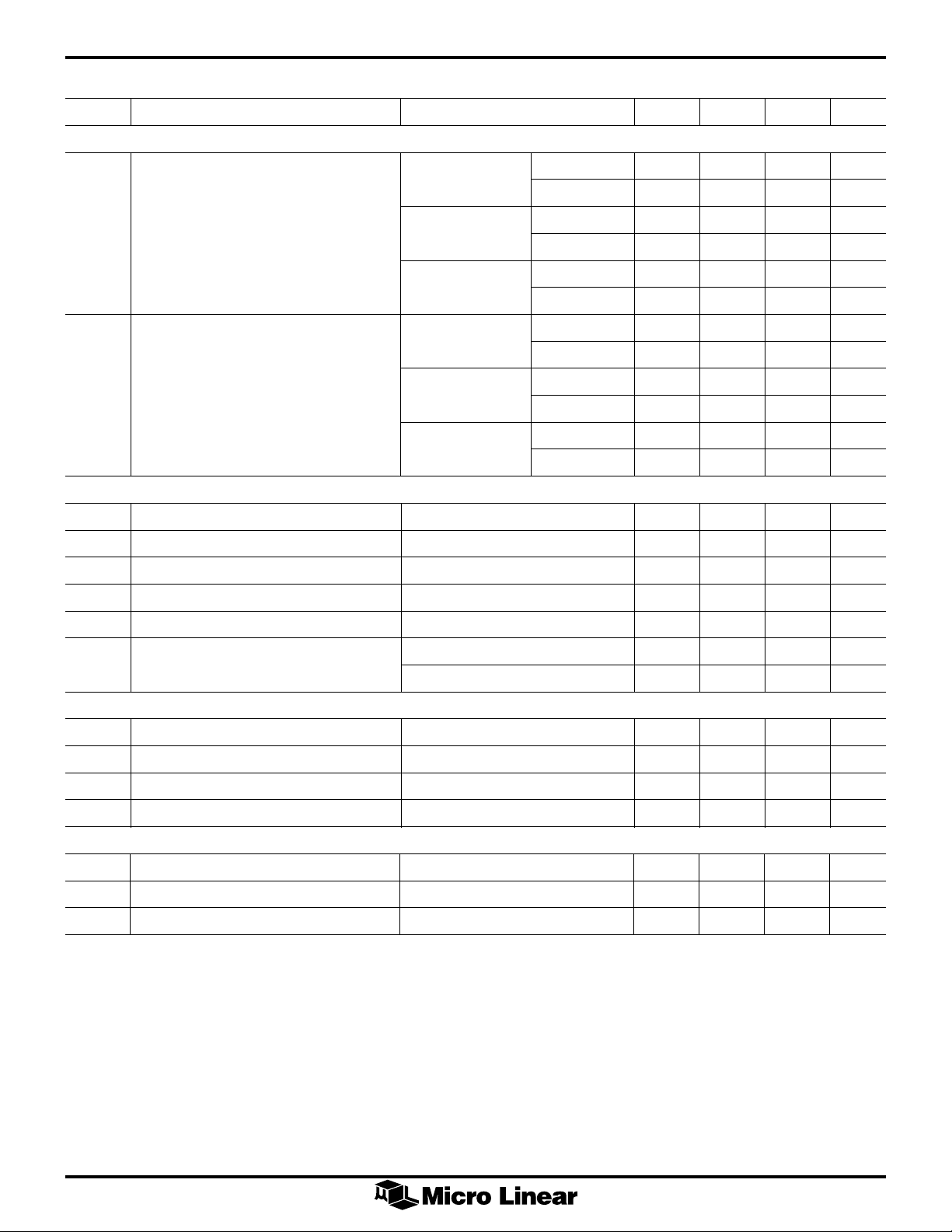
PIN DESCRIPTION
PIN NAME FUNCTION
1LP
A
Lowpass output for biquad A.
LP
BP
N/AP/HP
INV
S1
S
A/B
V
V
CLK
A
A
A
A
A
A+
D+
LSh
A
1
2
3
4
5
6
7
8
9
10
TOP VIEW
LP
20
B
BP
19
B
N/AP/HP
18
INV
17
S1
16
AGND
15
V
14
V
13
50/100/HOLD
12
CLK
11
PIN NAME FUNCTION
11 CLK
A-
D-
B
B
B
B
B
Clock input for biquad B.
2BP
A
Bandpass output for biquad A.
3 N/AP/HPANotch/allpass/highpass output for
biquad A.
4 INV
A
Inverting input of the summing op amp
for biquad A.
5S1
A
Auxiliary signal input pin used in
modes 1a, 1d, 4, 5, and 6b.
6S
A/B
7V
8V
A+
D+
Controls S2 input function.
Positive analog supply.
Positive digital supply.
9 LSh Reference point for clock input levels.
Logic threshold typically 1.4V above
LSh voltage.
10 CLK
A
Clock input for biquad A.
12 50/100/HOLDInput pin to control the clock-to-
center-frequency ratio of 50:1 or
100:1, or to stop the clock to hold the
last sample of the bandpass or lowpass
outputs.
13 V
14 V
D-
A-
Negative digital supply.
Negative analog supply.
15 AGND Analog ground.
16 S 1
B
Auxiliary signal input pin used in
modes 1a, 1d, 4, 5, and 6b.
17 INV
B
Inverting input of the summing op amp
for biquad B.
18 N/AP/HPBNotch/allpass/highpass output for
biquad B.
19 BP
20 L P
B
B
Bandpass output for biquad B.
Lowpass output for biquad B.
2

ABSOLUTE MAXIMUM RATINGS
ML2111
Absolute maximum ratings are those values beyond which
the device could be permanently damaged. Absolute
maximum ratings are stress ratings only and functional
device operation is not implied.
Lead Temperature (Soldering, 10 sec) ..................... 300ºC
Thermal Resistance (qJA)
20-Pin PDIP ...................................................... 67ºC/W
20-Pin SOIC ..................................................... 95ºC/W
Supply Voltage
|VA+|, |VD+| - |VA-|, |VD-| ...................................... 13V
OPERATING CONDITIONS
VA+, VD+ to LSh ..................................................... 13V
Inputs ......................|VA+, VD+| +0.3V to |VA-, VD-| -0.3V
Outputs ...................|VA+, VD+| +0.3V to |VA-, VD-| -0.3V
|VA+| to |VD+| ........................................................ ±0.3V
Junction Temperature .............................................. 150ºC
Temperature Range
ML2111CCX .............................................. 0ºC to 70ºC
ML2111CIP ............................................. -40ºC to 85ºC
Supply Range ........................................ ±2.25V to ±6.0V
Storage Temperature Range ...................... –65ºC to 150ºC
ELECTRICAL CHARACTERISTICS
Unless otherwise specified, VA+ = VD+ = 5V ± 10%, VA- = VD- = -5V ± 10%, CL = 25pF, V
Clock Duty Cycle = 50%, TA = Operating Temperature Range (Note 1)
SYMBOL PARAMETER CONDITIONS MIN TYP MAX UNITS
FILTER
f
0(MAX)
Maximum Center Frequency (Note 2) Figure 15 (Mode 1), 100 kHz
V
IN=1VPK
(0.707V
)Q £ 50, Q Accuracy £ ± 25%
RMS
Figure 15 (Mode 1), 150 kHz
Q £ 20, Q Accuracy £ ± 15%
= 1.41VPK (1.000V
IN
RMS
),
f
0(MIN)
f
CLK
V
OS2,3
Minimum Center Frequency (Note 2) Figure 15 (Mode 1), 25 Hz
V
IN=1VPK
f0 Temperature Coefficient f
Clock to Center Frequency Ratio 50:1, f
Q = 10, Figure 15 (Mode 1) C Suffix 49.45 49.85 50.25
Clock Frequency Q £ 20, Q Accuracy £ ±15% 2.5 7500 kHz
Clock Feedthrough f
Q Accuracy f
Q Temperature Coefficient f
DC Offset 50:1, f
(0.707V
)Q £ 50, Q Accuracy £ ± 30%
RMS
Figure 15 (Mode 1), 25 Hz
Q £ 20, Q Accuracy £ ± 15%
< 5MHz -10 ppm/ºC
CLK
= 5MHz B Suffix 49.65 49.85 50.05
CLK
100:1, f
CLK
CLK
50:1, Figure 15 (Mode 1) C Suffix ±5 %
f
CLK
100:1, Figure 15 (Mode 1) C Suffix ±8 %
CLK
S
A/B
100:1, f
S
A/B
= 5MHz B Suffix 99.6 100.0 100.4
CLK
£ 5MHz 10 20 mV
= 5MHz, Q = 10, B Suffix ±3 %
= 5MHz, Q = 10, B Suffix ±4 %
< 5MHz, Q = 10 20 ppm/ºC
= 5MHz B Suffix 7 40 mV
CLK
= High or Low C Suffix 7 60 mV
= 5MHz B Suffix 14 60 mV
CLK
=High or Low C Suffix 14 100 mV
C Suffix 99.2 100.0 100.8
(P-P)
3

ML2111
ELECTRICAL CHARACTERISTICS (Continued)
SYMBOL PARAMETER CONDITIONS MIN TYP MAX UNITS
FILTER (Continued)
Gain Accuracy, DC Lowpass R1,R3 = 20kW, R2 = 2kW, 0.01 2 %
100:1, f0 = 50kHz, Q = 10
Gain Accuracy, Bandpass at f
0
R1,R3 = 20kW, R2 = 2kW, B Suffix 1 4 %
100:1, f0 = 50kHz, Q = 10 C Suffix 1 6 %
Gain Accuracy, DC Notch Output R1,R3 = 20kW, R2 = 2kW, 0.02 2 %
100:1, f0 = 50kHz, Q = 10
Noise (Note 3) Bandpass 100kHz, 50:1 103 µV
Figure 15 (Mode 1), 50kHz, 100:1 121 µV
Q = 1, R1 = R2 = R3 = 2kW Lowpass 100kHz, 50:1 120 µV
Notch 100kHz, 50:1 115 µV
Noise (Note 3) Bandpass, 100kHz, 50:1 262 µV
Figure 15 (Mode 1), R1 = 20kW 50kHz, 100:1 333 µV
Q = 10, R3 = 20kW, R2 = 2kW Lowpass, 100kHz, 50:1 268 µV
R1 = 2kW 50kHz, 100:1 342 µV
Notch, 100kHz, 50:1 64 µV
R1 = 2kW 50kHz, 100:1 72 µV
Crosstalk f
= 5MHz, f0= 100kHz -50 dB
CLK
FILTER, VA+ = VD+ = 2.25V, VA- = VD- = -2.25V, VIN = 0.707 x VPK (0.5 x V
f
0(MAX)
Maximum Center Frequency Figure 15 (Mode 1), 75 kHz
Q £ 50, Q Accuracy £ ± 30%
50kHz, 100:1 150 µV
50kHz, 100:1 135 µV
)
RMS
RMS
RMS
RMS
RMS
RMS
RMS
RMS
RMS
RMS
RMS
RMS
RMS
f
0(MIN)
f
CLK
Figure 15 (Mode 1), 100 kHz
Q £ 20, Q Accuracy £ ± 15%
Minimum Center Frequency Figure 15 (Mode 1), 25 Hz
Q £ 50, Q Accuracy £ ± 30%
Figure 15 (Mode 1), 25 Hz
Q £ 20, Q Accuracy £ ± 15%
Clock to Center Frequency Ratio 50:1, f
= 2.5MHz B Suffix 49.65 49.85 50.05
CLK
Q = 10, Figure 15 (Mode 1) C Suffix 49.45 49.85 50.25
100:1, f
= 2.5MHz B Suffix 99.60 100.0 100.4
CLK
C Suffix 99.20 100.0 100.8
Clock Frequency Q £ 20, Q Accuracy £ ±15% 2.5 5000 kHz
Q Accuracy f
= 2.5MHz, Q = 10, B Suffix ±4 %
CLK
50:1, Figure 15 (Mode 1) C Suffix ±8 %
f
= 2.5MHz, Q = 10, B Suffix ±3 %
CLK
100:1, Figure 15 (Mode 1) C Suffix ±6 %
4
ML2111
ELECTRICAL CHARACTERISTICS (Continued)
SYMBOL PARAMETER CONDITIONS MIN TYP MAX UNITS
FILTER, VA+ = VD+ = 2.25V, VA- = VD- = -2.25V, VIN = 0.707 x VPK (0.5 x V
Noise (Note 3) Bandpass 100kHz, 50:1 105 µV
Figure 15 (Mode 1), 50kHz, 100:1 123 µV
Q = 1, R1 = R2 = R3 = 2kW Lowpass 100kHz, 50:1 122 µV
Notch 100kHz, 50:1 117 µV
Noise (Note 3) Bandpass, 100kHz, 50:1 265 µV
Figure 15 (Mode 1), Q = 10, R1 = 20kW 50kHz, 100:1 335 µV
R3 = 20kW, R2 = 2kW Lowpass, 100kHz, 50:1 270 µV
R1 = 2kW 50kHz, 100:1 245 µV
Notch, 100kHz, 50:1 65 µV
R1 = 2kW 50kHz, 100:1 73 µV
OPERATIONAL AMPLIFIERS
V
OS1
A
VOL
DC Offset Voltage 215mV
DC Open Loop Gain RL = 1kW 95 dB
Gain Bandwidth Product 2.4 MHz
) (Continued)
RMS
50kHz, 100:1 152 µV
50kHz, 100:1 138 µV
RMS
RMS
RMS
RMS
RMS
RMS
RMS
RMS
RMS
RMS
RMS
RMS
Slew Rate 2.0 V/µs
Output Voltage Swing (Clipping Level) RL = 2kW, |V| from VA+ or V
A-
Output Short Circuit Current Source 50 mA
Sink 25 mA
CLOCK
V
Input Low Voltage 0.6 V
CLK
V
Input High Voltage 3.0 V
CLK
CLKA, CLKB Pulse Width |VD+| - |VD-| ³ 4.5V 100 ns
CLKA, CLKB Pulse Width |VD+| - |VD-| ³ .90V 66 ns
SUPPLY
(IA+)+(ID+) Supply Current, (VA+) + (VD+)f
(IA-)+(ID-) Supply Current, (VA-) + (VD-)f
I
LSh
Note 1: Limits are guaranteed by 100% testing, sampling, or correlation with worst case test conditions.
Note 2: The center frequency is defined as the peak of the bandpass output.
Note 3: The noise is meassured with an HP8903A audio analyzer with a bandwidth of 700kHz, which is 7.5 times the f
Supply Current, LSh f
= 5MHz 13 22 mA
CLK
= 5MHz 12 21 mA
CLK
= 5MHz 0.5 1 mA
CLK
0.5 1.2 V
at 50:1 and 15 times the f0 at 100:1.
0
5

ML2111
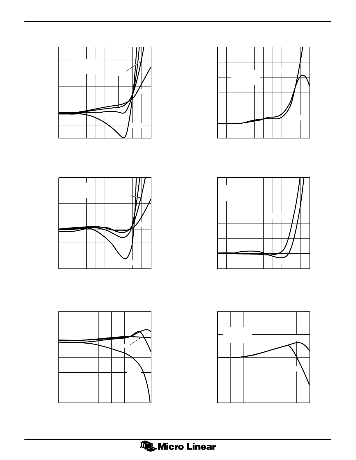
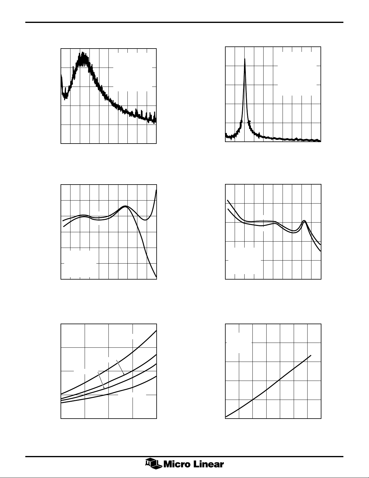
TYPICAL PERFORMANCE CURVES
0.4
0.0
RMS
f
CLK
Q = 20
(MHz)
Q = 50
Q = 10
–0.4
–0.8
–1.2
Deviation (%)
0
/f
–1.6
CLK
f
–2.0
–2.4
–2.8
04810
0.4
0.0
–0.4
–0.8
–1.2
Mode 1
T
= 25ºC
A
V
= 0.707V
IN
26
Q = 50
Q = 10
Q = 5
Figure 1A. f
Q = 20
CLK/f0
vs. f
Deviation (%)
0
/f
CLK
f
–1
–2
–3
(50:1, VS = ±5V)
CLK
0.5
0.0
–0.5
5
4
3
2
1
0
04810
Mode 1
Q = 10
V
= 0.707V
IN
26
RMS
f
CLK
TA = 85ºC
TA = 25ºC
(MHz)
TA = 25ºC
–1.6
Deviation (%)
0
/f
–2.0
CLK
f
–2.4
–2.8
–3.2
04810
16
14
12
10
8
Deviation (%)
6
0
/f
4
CLK
f
2
0
–2
0
0579
Mode 1
T
= 25ºC
A
V
= 0.707V
IN
26
V
16
RMS
f
(MHz)
CLK
Mode 1
T
= 25ºC
A
= 0.5V
IN
RMS
Q = 50
3
24
f
(MHz)
CLK
Q = 5
Figure 1B. f
Q = 10
Q = 20
Q = 5
8
CLK/f0
vs. f
Deviation (%)
0
–1.0
/f
CLK
f
–1.5
–2.0
(100:1, VS = ±5V)
CLK
10
8
6
4
Deviation (%)
0
/f
2
CLK
f
0
–2
Mode 1
Q = 10
V
= 0.707V
IN
04810
0619
26
Mode 1
Q = 10
V
= 0.5V
IN
RMS
RMS
f
CLK
f
CLK
TA = 85ºC
(MHz)
TA = 85ºC
(MHz)
TA = 25ºC
73
8254
Figure 1C. f
CLK/f0
vs. f
(50:1, VS = ±2.5V)
CLK
6

TYPICAL PERFORMANCE CURVES (Continued)
ML2111
5
4
3
2
Deviation (%)
1
0
/f
CLK
f
0
–1
–2
048
0.08
0.06
0.04
0.02
Mode 1
T
= 25ºC
A
V
= 0.5V
IN
RMS
2
1
f
(MHz)
CLK
V
Q = 50
Q = 20
Q = 10
Q = 5
7
63
5
Figure 1D. f
Mode 1
Q = 10
f
= 100kHz
0
f
= 5MHz
CLK
= 0.707V
IN
RMS
9
CLK/f0
vs. f
12
10
8
6
Deviation (%)
4
0
/f
CLK
f
2
0
–2
(100:1, VS = ±2.5V)
CLK
0.04
0.03
0.02
Mode 1
Q = 10
V
= 0.5V
IN
RMS
TA = 85ºC
TA = 25ºC
7
63
048
2
1
Mode 1
Q = 10
f
= 50kHz
0
f
= 5MHz
CLK
V
= 0.707V
IN
5
f
(MHz)
CLK
RMS
9
Deviation (%)
0.00
0
/f
CLK
f
–0.02
–0.04
–0.06
–40 20 60 100–20
Figure 2A. f
0.10
0.08
0.06
0.04
0.02
Deviation (%)
0
/f
0.00
CLK
f
–0.02
–0.04
40 800
Temperature (ºC)
Deviation vs. Temperature
CLK/f0
(50:1, VS = ±5V)
Mode 1
Q = 10
f
= 50kHz
0
f
= 2.5MHz
CLK
V
= 0.5V
IN
RMS
Deviation (%)
0
0.01
/f
CLK
f
0
–0.01
–40 20 60 100–20
Figure 2B. f
0.06
0.04
0.02
0.00
Deviation (%)
0
/f
–0.02
CLK
f
f
–0.04
CLK
V
Temperature (ºC)
Deviation vs. Temperature
CLK/f0
(100:1, VS = ±5V)
Mode 1
Q = 10
f
= 25kHz
o
= 2.5MHz
= 0.5V
IN
RMS
40 800
–0.06
–40 40 800
Figure 2C. f
20 60 100–20
Temperature (ºC)
Deviation vs. Temperature
CLK/f0
(50:1, VS = ±2.5V)
–0.06
–40 40 800
Figure 2D. f
20 60 100–20
Temperature (ºC)
Deviation vs. Temperature
CLK/f0
(100:1, VS = ±2.5V)
7
ML2111
TYPICAL PERFORMANCE CURVES (Continued)
20
16
12
8
4
Q Deviation (%)
0
–4
–8
04810
Mode 1
T
= 25ºC
A
V
= 0.707V
IN
26
RMS
f
CLK
Q = 10
Q = 20
Q = 50
(MHz)
Q = 5
Figure 2E. Q Error vs. f
20
Mode 1
T
V
= 0.707V
IN
= 25ºC
A
RMS
Q = 10
Q = 5
Q = 20
15
10
5
0
Q Deviation (%)
–5
20
16
12
8
Q Deviation (%)
4
0
–4
(50:1, VS = ±5V)
CLK
20
16
12
8
Q Deviation (%)
4
Mode 1
Q = 10
V
= 0.707V
IN
04810
26
Mode 1
Q = 10
V
= 0.707V
IN
RMS
RMS
f
CLK
TA = 25ºC
TA = 85ºC
(MHz)
TA = 85ºC
–10
–15
04810
26
f
CLK
Q = 50
(MHz)
Figure 2F. Q Error vs. f
10
5
0
–5
Q Deviation (%)
–10
–15
–20
Mode 1
T
= 25ºC
A
V
= 0.5V
IN
RMS
13 64
02 75
f
CLK
Q = 5
(MHz)
Q = 10
Q = 20
Q = 50
0
–4
(100:1, VS = ±5V)
CLK
8
4
0
Q Deviation (%)
–4
–8
TA = 25ºC
04810
02 75
26
f
(MHz)
CLK
Mode 1
Q = 10
V
= 0.5V
IN
RMS
TA = 85ºC
13 64
f
(MHz)
CLK
TA = 25ºC
Figure 2G. Q Error vs. f
(50:1, VS = ±2.5V)
CLK
8

TYPICAL PERFORMANCE CURVES (Continued)
ML2111
16
12
Mode 1
T
8
4
0
Q Deviation (%)
–4
–8
–12
02 75
= 25ºC
A
V
= 0.5V
IN
RMS
Q = 50
13 64
f
(MHz)
CLK
Figure 2H. Q Error vs. f
0.4
0.2
0.0
Q = 10
Q = 5
Q = 20
16
12
8
4
0
Q Deviation (%)
–4
–8
–12
02 75
(100:1, VS = ±2.5V)
CLK
0.6
0.4
0.2
0.0
Mode 1
Q = 10
V
= 0.5V
IN
RMS
13 64
f
(MHz)
CLK
TA = 85ºC
TA = 25ºC
–0.2
Q Deviation (%)
–0.4
–0.6
–0.8
–40 40 800
20 60–20
Temperature (ºC)
f
= 100kHz
0
f
CLK
V
= 0.707V
IN
Mode 1
Q = 10
= 5MHz
RMS
Figure 3A. Q Deviation vs. Temperature
(50:1, VS = ±5V)
0.2
0.0
Q Deviation (%)
–0.2
Mode 1
Q = 10
f
= 50kHz
0
f
= 2.5MHz
CLK
V
= 0.5V
IN
RMS
100
–0.2
–0.4
Q Deviation (%)
–0.6
–0.8
–1.0
–40 40 800
20 60 100–20
Temperature (ºC)
f
0
f
CLK
V
= 0.707V
IN
Mode 1
Q = 10
= 50kHz
= 5MHz
RMS
Figure 3B. Q Deviation vs. Temperature
(100:1, VS = ±5V)
0.2
0.0
Q Deviation (%)
–0.2
Mode 1
Q = 10
f
= 25kHz
0
f
= 2.5MHz
CLK
V
= 0.5V
IN
RMS
–0.4
–40 40 800
20 60 100–20
Temperature (ºC)
Figure 3C. Q Deviation vs. Temperature
(50:1, VS = ±2.5V)
–0.4
–40 40 800
20 60 100–20
Temperature (ºC)
Figure 3D. Q Deviation vs. Temperature
(100:1, VS = ±2.5V)
9
ML2111
TYPICAL PERFORMANCE CURVES (Continued)
4
Mode 1
T
= 25ºC
A
f
= 5MHz
CLK
V
= 1V
IN
RMS
0
100:1
Deviation (%)
0
/f
–4
CLK
f
–8
0.1 1 10 100
50:1
Ideal Q (R3/R2)
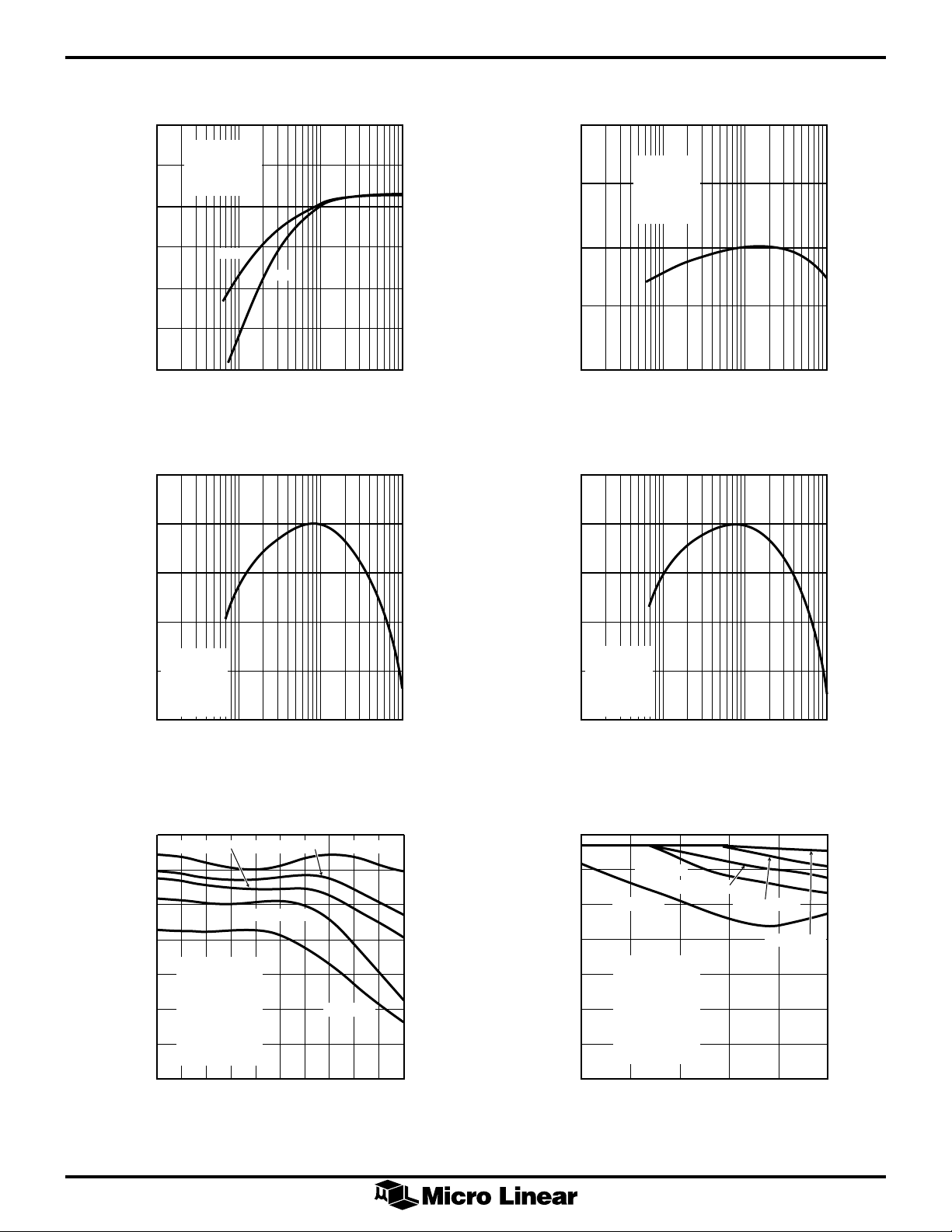
Figure 4A. f
Deviation vs. Q (VS = ±5V) Figure 4A. f
CLK/f0
4
0
–4
0.05
Mode 1
T
= 25ºC
A
50:1 or 100:1
f
= 5MHz
CLK
V
= 1V
IN
RMS
0.0
Deviation (%)
0
/f
CLK
f
–0.05
0.1 1 10 100
Ideal Q (R3/R2)
CLK/fNOTCH
Deviation vs. Q (VS = ±5V)
2
0
–2
–8
Q Deviation (%)
Mode 1
T
–12
–16
= 25ºC
A
f
= 100kHz
0
f
= 5MHz
CLK
V
= ±5V
S
0.1 1 10 100
Ideal Q (R3/R2)
Figure 5A. Q Deviation vs. Q (50:1, VS = ±5V)
70
V
= 2V
V
OUT
OUT
= 1.41V
60
50
V
= 3V
OUT
40
30
20
10
Single Frequency Distortion Level (dB)
0
04080
Mode 1
Q = 1
f
= 100kHz
0
f
= 5MHz
CLK
V
= ±5V
S
T
= 25ºC
A
R
= 2kΩ
L
Low Pass Output
20
fIN (kHz)
V
= 0.5V
OUT
V
= 4V
OUT
10060
–4
Q Deviation (%)
Mode 1
T
= 25ºC
A
–6
f
= 50kHz
0
f
= 5MHz
CLK
V
= ±5V
S
–8
0.1 1 10 100
Ideal Q (R3/R2)
Figure 5B. Q Deviation vs. Q (100:1, VS = ±5V)
70
V
60
50
40
30
20
10
Single Frequency Distortion Level (dB)
0
02040
= 3V
OUT
V
= 4V
OUT
Mode 1
Q = 1
f
= 50kHz
0
f
= 5MHz
CLK
V
= ±5V
S
T
= 25ºC
A
R
= 2kΩ
L
Low Pass Output
10
V
= 2V
OUT
fIN (kHz)
V
OUT
= 1.41V
V
OUT
= 0.5V
5030
Figure 6A. Distortion vs. fIN (50:1, VS = ±5V) Figure 6B. Distortion vs. fIN (100:1, VS = ±5V)
10
TYPICAL PERFORMANCE CURVES (Continued)
ML2111
250
Mode 1
50:1
200
150
100
Noise (nV/√Hz)
50
0
0 200 300 500400100
Frequency (kHz)
R1 = R2 = R3 = 2kΩ
BANDPASS OUTPUT
V
= ±5V
S
f
= 100kHz
0
f
= 5MHz
CLK
Figure 7A. Noise Spectrum Density (Q = 1)
0.8
0.4
0.0
–0.4
Deviation (%)
Notch
/f
CLK
f
–0.8
–1.2
–1.6
Mode 1
T
= 25ºC
A
Q = 10
V
S
V
= 0.707V
IN
04810
100:1
50:1
= ±5V
RMS
26
f
(MHz)
CLK
2500
Mode 1
50:1
2000
1500
1000
Noise (nV/√Hz)
500
0
0 200 300 500400100
Frequency (kHz)
R1 = R3 = 20kΩ,
R2 = 2kΩ
BANDPASS OUTPUT
V
= ±5V
S
f
= 100kHz
0
f
= 5MHz
CLK
Figure 7B. Noise Spectrum Density (Q = 10)
100
80
60
40
Notch Depth (dB)
20
Mode 1
T
= 25ºC
A
Q = 10
V
= ±5V
S
V
= 0.707V
IN
0
04810
100:1
50:1
RMS
26
f
(MHz)
CLK
Figure 8. f
16
Q = 10
T
= 25ºC
A
L
= V
Sh
50:1
14
12
Supply Current (mA)
10
8
234 65
SS
f
CLK
= 3MHz
CLK/fNOTCH
f
= 5MHz
CLK
Supply Voltage (±V)
vs. f
f
CLK
f
CLK
CLK
= 10MHz
= 250kHz
Figure 10. Supply Current vs. Supply Voltage
Figure 9. Notch Depth vs. f
15
Mode 1
V
= ±5V
S
14
f
= 5MHz
CLK
50:1
13
12
Supply Current (mA)
11
10
–40 20 60 100–20
Temperature (ºC)
40 800
CLK
Figure 11. Supply Current vs. Temperature
11

ML2111
FUNCTIONAL DESCRIPTION
POWER SUPPLIES
f
CLK/f0
RATIO
The analog (VA+) and digital (VD+) supply pins, in most
cases, are tied together and bypassed to AGND with
100nF and 10nF disk ceramic capacitors. The supply pins
can be bypassed separately if a high level of digital noise
exists. These pins are internally connected by the IC
substrate and should be biased from the same DC source.
The ML2111 operates from either a single supply from 4V
to 12V, or with dual supplies at ±2V to ±6V.
CLOCK INPUT PINS AND LEVEL SHIFT
With dual supplies equal to or higher than ±4.0V, the LSh
pin can be connected to the same potential as either the
AGND or the VA- pin. With single supply operation the
negative supply pins and LSh pin should be tied to the
system ground. The AGND pin should be biased half way
between VA+ and VA-. Under these conditions the clock
levels are TTL or CMOS compatible. Both input clock
pins share the same level shift pin.
50/100/HOLD
Tying the 50/100/HOLD pin to the VA+ and VD+ pins
makes the filter operate in the 50:1 mode. Tying the pin
half way between VA+ and VA- makes the filter operate in
the 100:1 mode. The input range for 50/100/HOLD is
either 2.5V ±0.5V with a total power supply range of 5V,
or 5V ±0.5V with a total power supply range of 10V.
When 50/100/HOLD is tied to the negative power supply
input, the filter operation is stopped and the bandpass and
lowpass outputs act as a sample/hold circuit which holds
the last sample.
S1A & S1
These voltage signal input pins should be driven by a
source impedance of less than 5kW. The S1A and S1B pins
can be used to feedforward the input signal for allpass
filter configurations (see modes 4 & 5) or to alter the
clock-to-center-frequency ratio (f
modes 1b, 1c, 2a, & 2b). When these pins are not used
they should be tied to the AGND pin.
S
A/B
When S
summing device is tied to the lowpass output. When the
S
A/B
switches to ground.
AGND
B
) of the filter (see
CLK/f0
is high, the S2 negative input of the voltage
A/B
pin is connected to the negative supply, the S2 input
The ML2111 is a sampled data filter and approximates
continuous time filters. The filter deviates from its ideal
continuous filter model when the (f
and when the Qs are low.
f0 ´ Q PRODUCT RATIO
The f0 ´ Q product of the ML2111 depends on the clock
frequency and the mode of operation. The f0 ´ Q product
is mainly limited by the desired f0 and Q accuracy for
clock frequencies below 1MHz in mode 1 and its
derivatives. If the clock to center frequency ratio is
lowered below 50:1, the f0 ´ Q product can be further
increased for the same clock frequency and for the same
Q value.
Mode 3, (Figure 23) and the modes of operation where R4
is finite, are "slower" than the basic mode 1. The resistor
R4 places the input op amp inside the resonant loop. The
finite GBW of this op amp creates an additional phase
shift and enhances the Q value at high clock frequencies.
OUTPUT NOISE
The wideband RMS noise on the outputs of the ML2111 is
nearly independent of the clock frequency, provided that
the clock itself does not become part of the noise. Noise
at the BP and LP outputs increases for high values of Q.
) ratio decreases
CLK/f0
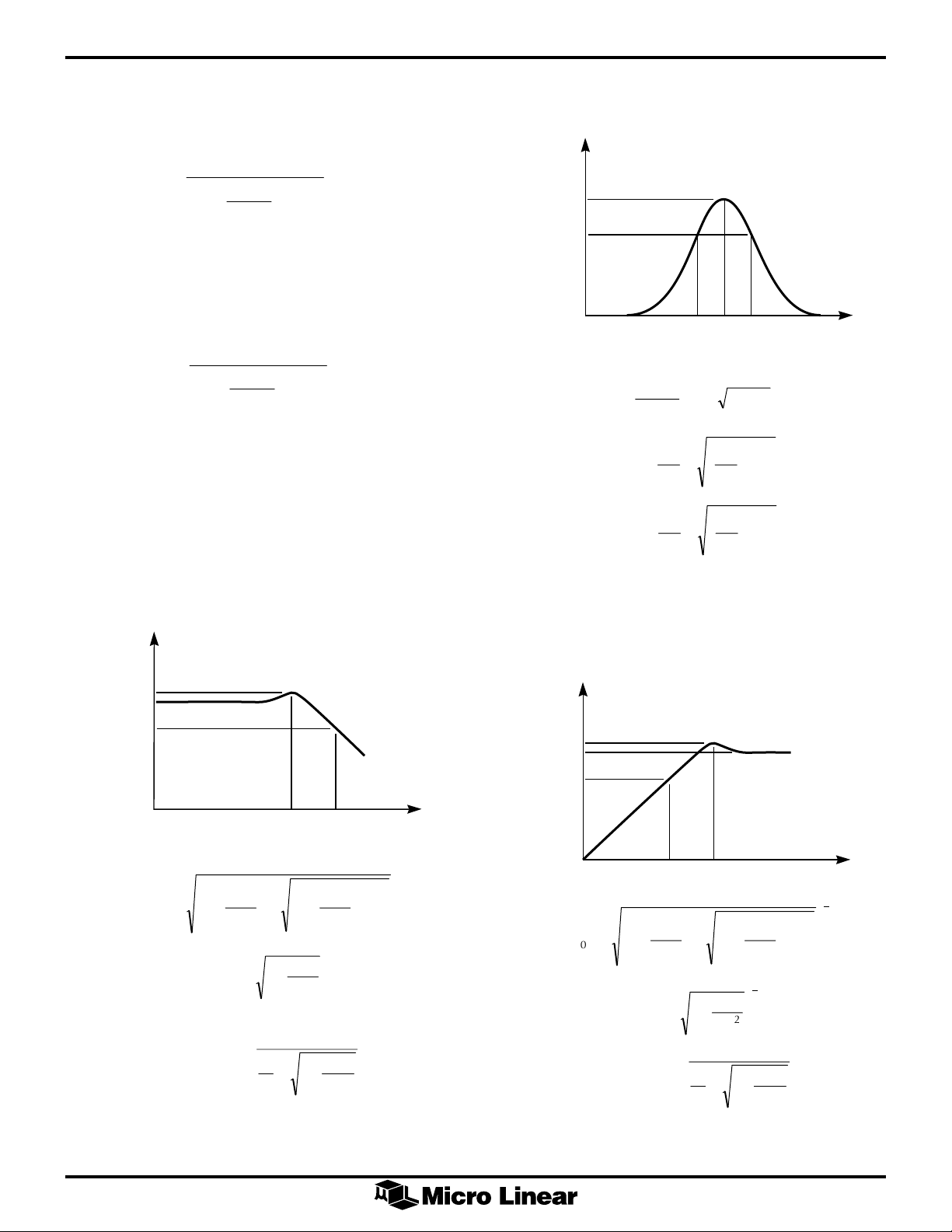
FILTER FUNCTION DEFINITIONS
Each filter of the ML2111, along with external resistors
and a clock, approximates second order filter functions.
These are tabulated below in the frequency domain.
1. Bandpass function: available at the bandpass output
pins (BPA, BPB), Figure 12.
s
w
0
Gs H
()=
OBP
where:
H
= Gain at w = w
OBP
f0 = w0/2p. The center frequency of the complex pole
pair is f0. It is measured as the peak frequency of the
bandpass output.
20
s
Q
s
w
+
Q
0
2
+
w
0
(1)
AGND is connected to the system ground for dual supply
operation. When operating with a single positive supply
the analog ground pin should be biased half way between
VA+ and VA-, and bypassed with a 100nF capacitor. The
positive inputs of the internal op amps and the reference
point of the internal switches are connected to the AGND
pin.
12
Q = the Quality factor of the complex pole pair. It is
the ratio of f0 to the -3dB bandwidth of the 2nd order
bandpass function. The Q is always measured at the
filter BP output.
FILTER FUNCTION DEFINITIONS (Continued)
ML2111
2. Lowpass function: available at the LP output pins,
Figure 13.
2
w
Gs H
()=
OLP
where:
H
= DC gain of the LP output
OLP
3. Highpass function: available only in mode 3 at
N/AP/HPA and N/AP/HPB, Figure 14.
Gs H
()=
OHP
H
= Gain of the HP output for f ® f
OHP
20
s
+
20
s
0
s
w
+
Q
2
s
w
s
Q
2
+
w
0
2
w
+
0
CLK
/2.
(2)
(3)
H
0.707 H
GAIN (V/V)
OBP
OBP
Q
ff
=-+
L
ff
= +
H
BANDPASS OUTPUT
f
f
f
0
H
=
LH
2
2
2
2
f (LOG SCALE)
f
0
=
ff
-
HL
121
0
QQ
121
0
QQ
L
fff
;
0
+
1
1
+
H
H
0.707 H
GAIN (V/V)
ff
LOWPASS OUTPUT
OP
OLP
OLP
= -
C
0
ff
HH
=
OP OLP
f
P
f (LOG SCALE)
1
1
QQ
2
= -
P
0
+-
22
1
2
1
-
Q
f
C
1
1
2
1
2
Q
1
1
1
2
Q
4
2
+
1
H
H
OHP
0.707 H
OHP
GAIN (V/V)
ff
C
Figure 12.
HIGHPASS OUTPUT
OP
= -
0
1
!
HH
OP OHP
2
ff
= -
P
0
=
f
f
C
P
f (LOG SCALE)
1
QQ
+-
1
22
!
1
Q
2
1
-
Q
1
1
2
1
-
"
#
2
#
$
1
1
1
2
Q
4
-
1
"
2
#
+
1
#
#
$
Figure 13.
Figure 14.
13

ML2111
FILTER FUNCTION DEFINITIONS
4. Notch function: available at N/AP/HPA and N/AP/HP
for several modes of operation.
2
s
Gs H
()=
ON
2
H
= Gain of the notch output for f ® f
ON2
H
= Gain of the HP output for f ® 0
ON1
49
s
20
s
+
fn = wn/2p. The frequency of the notch occurrence is
fn.
5. Allpass function: available at N/AP/HPA and N/AP/
HPB for modes 4 and 4a.
s
20
s
-
Gs H
()=
OAP
H
= Gain of the allpass output for 0 < f < f
OAP
s
2
s
+
For allpass functions, the center frequency and the Q of
the numerator complex zero pair is the same as the
denominator. Under these conditions the magnitude
response is a straight line. In mode 5, the center
frequency fZ of the numerator complex zero pair is
different than f0. For high numerator Q's, the
magnitude response will have a notch at fZ.
2
+
w
n
w
+
w
Q
w
+
w
Q
w
Q
0
0
+
w
0
2
0
2
2
CLK
/2.
CLK
(4)
(5)
/2
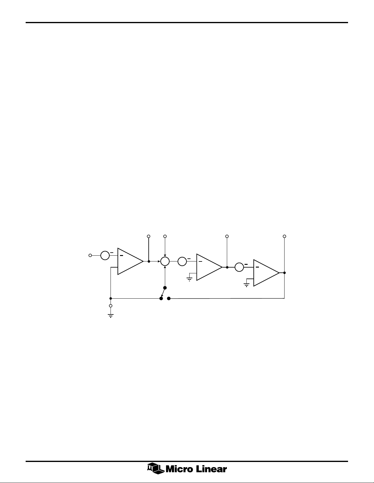
OPERATION MODES
B
There are three basic modes of operation — Modes 1, 2,
and 3 , each of which has derivatives; and four secondary
modes of operation — Modes 4, 5, 6, and 7, each of
which also has derivatives.
In Figure 15, the input amplifier is outside the resonant
loop. Because of this, mode 1 and its derivatives (modes
1a, 1b, 1c, and 1d) are faster than modes 2 and 3.
Mode 1 provides a clock tunable notch. It is a practical
configuration for second order clock tunable bandpass/
notch filters. In mode 1, a band pass output with a very
high Q, together with unity gain can be obtained with the
dynamics of the remaining notch and lowpass outputs.
Mode 1a (Figure 16) represents the simplest hookup of the
ML2111. It is useful when voltage gain at the bandpass
output is required. However, the bandpass voltage gain is
equal to the value of Q, and second order, clock tunable,
BP resonator can be achieved with only 2 resistors. The
filter center frequency directly depends on the external
clock frequency. Mode 1a is not practical for high order
filters as it requires several clock frequencies to tune the
overall filter response.
Modes 1b and 1c, Figures 17 and 18, are similar. They
both produce a notch with a frequency which is always
equal to the filter center frequency. The notch and the
center frequency can be adjusted with an external resistor
ratio.
½ ML2111 ½ ML2111
R3
R2
R1
V
IN
4 (17)
+
S
A/B
6
f
= = =- =-
15
V+
f
CLK
ffH
;; ; ;
100 50 1 1
nOLP OBP00
()
H
ON1
N
3 (18)
+
R2
=- =;
R
1
Q
Σ
S1
A
5 (16)
R2
R
R3
R2
BP
2 (19) 1 (20)
H
LP
R3
R
Figure 15. Mode 1: 2nd Order Filter Providing Notch,
Bandpass, Lowpass
V
R3
R2
4 (17)
+
S
A/B
6
V+
15
f
f
H non inverting H
CLK
===-
100 50
()
11=- =-();
OBP OLP2
IN
BP2
S1
A
5 (16)
3 (18)
+
Σ
R3
Q
;; ;
H
OBP01
R2
BP1
2 (19)
R3
R2
Figure 16. Mode 1a: 2nd Order Filter Providing
Bandpass, Lowpass
LP
1 (20)
14
ML2111
MODE BPA, BP
B
6a LP HP
6b LP LP
7LPAP
Table 1. First Order Functions.
MODE LPA, LP
B
BPA, BP
B
N/AP/HP
1 LP BP Notch
1a LP BP BP
1b LP BP Notch
N/AP/HPA, N/AP/HP
A&B
f
CLK
100 50()
f
CLK
100 50()
f
CLK
100 50
B
f
1
+
f
C
f
CLK
100 50()
f
CLK
100 50()
f
CLK
100 50()
0
R
RR
56()
+
R2
R3
R2
R3
R2
R3
6
f
CLK
100 50
f
Z
f
CLK
100 5 0()
f
N
f
0
1
+
R2
R3
R
6
RR
56()
+
1c LP BP Notch
1d LP BP
2 LP BP Notch
2a LP BP Notch
2b LP BP Notch
3LPBPHP
3a LP BP Notch
4LP BPAP
f
CLK
f
CLK
100 50
100 50()
f
CLK
100 50
100 50
100 50 4656()
100 50 4()
100 50 4()
+
f
CLK
+ +
f
CLK
+
f
CLK
f
CLK
f
CLK
100 50()
R
6
RR
56()
+
R2
1
R
4()
R2
1
RRRR
4656()
+
R2
RRRR
+
R2
R
R2
R
f
CLK
100 50
f
CLK
100 50()
f
CLK
100 50
f
CLK
100 50
f
CLK h
100 50()
R
+
6
RR
56()
+
1
RR
R
6
RR
56()
+
R
R
l
R
56()
+
6
4a LP BP AP
5LP BPCZ
Table 2. Second Order Functions
f
CLK
100 50 4()
100 50
f
CLK
+
R2
R
1
R2
R
f
CLK
4()
100 50
R2
1
-
R
4()
15

ML2111
/
/
Σ
S1
A
5 (16)
R5
BP
2 (19)
LP
1 (20)
f
f
Q
Hf H f
H
CLK
=+
100 50
()
R3
R2
=
16
ON ON
12
=- =
OBP OLP
RR
0
R3
H
;
R
R
1
56
6
RR
56
+
R
6
Rk=+
+
++1
16 5 6
ff
=
;
n00
<1
55; W
f
CLK
21
R2 R
-
RRR
/
=-
1
0
R2
R
5
R6
R3
R2
V
R1
IN
4 (17)
+
S
A/B
6
V+
15
N
3 (18)
+
Figure 17. Mode 1b: 2nd Order Filter Providing Notch, Bandpass, Lowpass
Σ
S1
A
5 (16)
R5
BP
2 (19)
LP
1 (20)
f
f
Q
Hf H f
CLK
=
100 50
()
R3
=
R2RRR
0
=
16
ON ON
12
R
6
RR
56
+
6
;
+
56
ff
=
;
n00
f
CLK
21
=-
R2
R
;
R6
R3
R2
V
R1
IN
4 (17)
+
N
3 (18)
+
S
A/B
6
V-
15
H
OBP OLP
R3
=- =
H
R
1
R2 R
-
1
RRR
+
656
/
0
5
Rk
<
55;
;
W
Figure 18. Mode 1c: 2nd Order Filter Providing Notch, Bandpass, Lowpass
R3B
R2
V
R1
IN
4 (17)
+
S
A/B
6
V+
15
N
3 (18)
+
Σ
S1
A
5 (16)
R3A
BP
2 (19)
LP
1 (20)
f
f
H
CLK A
==+=-
100 50
=- -
OLP N IN
Q
;; ;
()
R2
V
;
R
11
R3
R3
H
OBP0
B
V
1
R2
R
R2
R
Q
1
Figure 19. Mode 1d: 2nd Order Filter Providing Bandpass and Lowpass for Qs Greater Than or Equal To 1.
16

R4
/
/
/
ML2111
R3
R2
V
V
R1
IN
IN
6
R1
6
S
S
V+
V+
A/B
A/B
4 (17)
4 (17)
+
15
Figure 20. Mode 2: 2nd Order Filter Providing Notch, Bandpass, Lowpass
R4
R3
R2
+
15
Figure 21. Mode 2a: 2nd Order Filter Providing Notch, Bandpass, Lowpass
3 (18)
R6
3 (18)
N
S1
A
5 (16)
+
Σ
R5
N
S1
A
5 (16)
+
Σ
BP
2 (19)
BP
2 (19)
LP
1 (20)
LP
1 (20)
f
CLK
=+=
f
0
100 50
()
R3
Q
=+ =
H
OBP ON
Hf
ON
=++
f
f
=+
n
Q
=++
Hf
ON1
H
OLP
1
R2
R3
-
=
R
f
CLK
2
21
f
CLK
100 50
()
f
CLK
100 50
()
R3
1
R2
0
=-
16
=
14656
R2 R R R R
+++
0
R2
1
;
4 100 50
R
R2
H
;
OLP
R
4
Hf
;
=
16
1
R2
-
=
R
R2
1
4656 1
RRRR
R
1
RR
+
56 2 1
R2
RRRR
4
56
%
R2
&
R
1
14656
+++
'
R2 R
-
//
5
f
CLK
f
n
-
+
14
0
14
+
6
Hf
;;
6
;
+
RRR
16 5 6
++
R2 R R R R
//
05
1
0
;
()
R2 R
1
/
R2 R
0
R2 R
-
+1
0
ON
;
/
5
1
R2 R
;;
2
/
;
/
5
R3
=-
H
OBP0
05
R
f
CLK
R2
=-
R
(
;
)
*
5
R4
f
f
f
LP
Hf
Hf
H
Σ
R5
S1
A
5 (16)
BP
2 (19)
1 (20)
R6
R3
R2
V
R1
IN
4 (17)
+
S
A/B
6
V-
15
Figure 22. Mode 2b: 2nd Order Filter Providing Notch, Bandpass, Lowpass
N
3 (18)
+
CLK
=+
0
100 50 4656
f
CLK
=
n
=-
16
ON1
ON
=
OLP
R2 R R R R
05 0 5
R2
RRRR
R
6
RR
+
56 4
%
R2
0
f
CLK
21 1
//
&
R
R2 R R R R
1
05
'
R2
=- =-;;
R
R2 R
-
++
4656
;
+()
R3R2R2
Q
= +
;;
/
RRR
656
//
4656
H
OBP2
1
RRRR
+
05
++
R3
R
6
+100 50
56()
(
;
)
*
17

ML2111
OPERATION MODES (Continued)
The clock to center frequency ratio range is:
f
500
1
100150
or
100150
CLK
f
0
f
CLK
1
f
0
or
(mode 1c) (6)
1
100250
or
(mode 1b) (7)
2
The input impedance of the S1 pin is clock dependent,
and in general R5 should not be larger than 5kW for f
2.5MHz and 2kW for f
> 2.5MHz. Mode 1c can be
CLK
CLK
used to increase the clock-to-center-frequency ratio
beyond 100:1. The limit for the (f
) ratio is 500:1 for
CLK/f0
this mode. The filter will exhibit large output offsets with
larger ratios. Mode 1d (Figure 19) is the fastest mode of
operation: center frequencies beyond 20kHz can easily
be achieved at a 50:1 ratio.
R4
R3
R2
V
R1
IN
4 (17)
+
HP
3 (18)
+
Σ
S1
A
5 (16)
BP
2 (19)
<
Modes 2, 2a, and 2b (Figures 20, 21, and 22) have notch
outputs whose frequency, fn, can be tuned independently
from the center frequency, f0. However, for all cases fn <
f0. These modes are useful when cascading second order
functions to create an overall elliptic highpass, bandpass
or notch response. The input amplifier and its feedback
resistors R2 and R4 are now part of the resonant loop.
Because of this, mode 2 and its derivatives are slower
than mode 1 and its derivatives.
In Mode 3 (Figure 23) a single resistor ratio, R2/R4, can
tune the center frequency below or above the f
f
/50) ratio. Mode 3 is a state variable configuration
CLK
since it provides a highpass, bandpass, lowpass output
through progressive integration. Notches are acquired by
summing the highpass and lowpass outputs (mode 3a,
Figure 24). The notch frequency can be tuned below or
LP
1 (20)
f
f
H
CLK
==
0
100 50 4 4
()
=- =- =-
OHP OLP OBP
R2
R
R2
H
;;
R
1
R3R2R2
Q
;;
R
4
H
R
11
R
CLK
R3
R
/100 (or
S
A/B
6
V-
15
Figure 23. Mode 3: 2nd Order Filter Providing Highpass, Bandpass, Lowpass — ½ ML2111
R2RR3
Q
=
R4
R3
R2
V
R1
IN
4 (17)
+
S
A/B
6
V-
15
HP
3 (18)
+
Σ
S1
A
5 (16)
BP
2 (19)
R
h
LP
1 (20)
R
l
+
H
Hff Q
ON
R
g
External
Op Amp
f
CLK
==
f
0
100 50 4 100 50
()
R2
=- =- =-
OHP OBP OLP
== -
16
0
NOTCH
R2
R
H
;;;
R
11
R
g
R
l
Hf
2
ON
Hf
ON
f
;
H
CLK h
f
n
()
R3
H
R
R
OLP
1
g
R
h
f
CLK
=;
21
0
=
16
4
R
H
OHP
R
g
RR2R
h
R
g
R
l
R2
R
;
R
l
4
R
1
;
4
R
1
R
Figure 24. Mode 3a: 2nd Order Filter Providing Highpass, Bandpass, Lowpass, Notch — ½ ML2111
18

OPERATION MODES (Continued)
ML2111
above the center frequency through the resistor ratio Rh/
Rl. Because of this, modes 3 and 3a are the most versatile
and useful modes for cascading second order sections to
obtain high order elliptic filters. For very selective
bandpass/bandreject filters the mode 3a approach , as in
Figure 24, yields better dynamic range since the external
op amp helps to optimize the dynamics of the output
nodes of the ML2111.
Modes 4 and 5 are useful for constructing allpass response filters. Mode 4, Figure 25, gives an allpass
response, but due to the sampled nature of the filter, a
slight 0.5 dB peaking can occur around the center
R3
R2
R1 = R2
V
IN
4 (17)
+
S
A/B
6
15
frequency. Mode 4a (Figure 26) gives a non-inverting
output, but requires an external op amp. Mode 5 is
recommended if this response is unacceptable. Mode 5
(Figure 27) gives a flatter response than mode 4 if R1 = R2
= 0.02 ´ R4.
Modes 6 and 7 are used to construct 1st order filters.
Mode 6a (Figure 28) gives a lowpass and a highpass
single pole response. Mode 6b (Figure 29) gives an
inverting and non-inverting lowpass single pole filter
response. Mode 7 (Figure 30) gives an allpass and lowpass
single pole response.
AP
3 (18)
+
Σ
S1
A
5 (16)
BP
2 (19) 1 (20)
LP
V+
f
o
=
100 50
f
CLK
05
R
3
Q
=
;
H
;
OAP
R
2
R
2
=
-
;
H
OLP
R
1
=-
2
H
;
OBP
R
3
=
-
2
R
2
Figure 25. Mode 4: 2nd Order Filter Providing Allpass, Bandpass, Lowpass — ½ ML2111
R4
R3
f
CLK
==
f
R2
V
IN
R1
4 (17)
+
S
A/B
6
15
HP
3 (18)
+
Σ
S1
A
5 (16)
BP
2 (19)
LP
1 (20)
R
R5
External
Op Amp
0
100 50 4 4
()
R
H
OAP OHP
H
OLP
H
OBP
5
==-
R
21
R
=-
=-
R2
R
H
;;
4
;
R
1
R3R2R2
;;
Q
R
R2
R
R3
R
1
V-
2R
+
Figure 26. Mode 4a: 2nd Order Filter Providing Highpass, Bandpass, Lowpass, Allpass — ½ ML2111
19

ML2111
R4
R3
R2
V
R1
IN
H
4 (17)
+
S
A/B
6
=+=-
f
0
OBP OZ
15
V+
f
CLK
100 50
()
R3
Q
=+ =-1
R2
R3
R2
1
=+
CZ
S1
A
5 (16)
3 (18)
+
Σ
R2
1
;
410050
R
R2
Q
;;
R
41
R2
Hf
;
R
1
f
f
CLK
Z
()
R3
Z
R
=
0
16
1
RR
05
RR2
0
BP
LP
2 (19)
1 (20)
1
R
1
;
4
R
R
1
R
4
-
411
/
41
/
;
+
5
R3
V
IN
R2
R1
4 (17)
+
S
A/B
6
f
C
15
V-
f
CLK
= =- =-
100 50 1 1()
HP
S1
A
5 (16)
3 (18)
+
Σ
R2
H
;;
OLP OHP
R3
R3
R
2 (19) 1 (20)
H
LP
Figure 28. Mode 6a: 1st Order Filter Providing
Highpass, Lowpass — ½ ML2111
R2
R
Hf
OZ
f
CLK
R2
H
==
;
OLP
R
11
14
/
05
R2 R
+21
/
0
5
R2 R
+
Figure 27. Mode 5: 2nd Order Filter Providing
Numerator Complex Zeroes, Bandpass, Lowpass — ½
ML2111
V
LP1
3 (18)
+
Σ
IN
5 (16)
S1
A
LP2
2 (19)
1 (20)
R3
R2
4 (17)
+
S
A/B
6
15
R3
R2 = R1
R1 = R2
V
IN
4 (17)
+
S
A/B
6
15
AP
3 (18)
+
Σ
S1
A
5 (16)
LP
2 (19)
1 (20)
V-
f
f
CLK
= ==-
C
100 50
()
R2
HH
;;
R3
1
OLP OLP
12
R3
R2
Figure 29. Mode 6b: 1st Order Filter Providing Lowpass
— ½ ML2111
20
V-
f
ff
== =-
PZ
CLK
100 502()
|GAIN AT OUTPUT| = 1 FOR
R2
R3
H
;
OLP
02f
R2
R3
f
CLK
Figure 30. Mode 7: 1st Order Filter Providing Allpass,
Lowpass — ½ ML2111

ML2111
HP
INV
CLK
BP
V
20
LP
B
B
B
B
S1
B
R32
19
R22
18
17
16
15
Q1 = 0.541
14
-
V
A
13
-
D
12
Q2 = 1.302
-5V
5V
11
B
V
OUT
0
–10
–20
–30
(dB)
IN
–40
/V
OUT
–50
V
–60
–70
–80
10k 100k 1M
FREQUENCY (Hz)
V
IN
1V
5V
Clock 5MHz
R31
R21
p-p
1
LP
A
2
BP
A
3
HP
A
4
INV
A
5
S1
A
6
S
AGND
A/B
7
VA+
8
+
V
D
9
LSh
CLK
50/100
A
10
1% RESISTOR VALUES
R21 = 3746Ω
R31 = 2003Ω
R22 = 1996Ω
R32 = 2604Ω
Figure 31. 4th Order, 100kHz Lowpass Butterworth Filter Obtained by Cascading Two Sections in Mode 1a.
101,777Hz
–3.058dB
V
OUT
0
–10
–20
149,871Hz
–30
(dB)
IN
–40
/V
OUT
–50
V
–60
–70
–80
10k 100k 1M
FREQUENCY (Hz)
–0.31dB
V
IN
2.82V
(1V
RMS
p-p
)
R11
5V
Clock 7.5MHz
R31
R21
BP
HP
INV
V
CLK
20
LP
B
19
B
18
B
17
B
16
S1
B
15
14
-
V
A
13
-
D
12
R12
R32
R22
Q1 = Q2 = 10
-5V
5V
11
B
1
LP
A
2
BP
A
3
HP
A
4
INV
A
5
S1
A
6
S
AGND
A/B
7
VA+
8
+
V
D
9
LSh
CLK
50/100
A
10
RESISTOR VALUES
R11 = 20kΩ
R21 = 2kΩ
R31 = 20kΩ
R12 = 20kΩ
R22 = 2kΩ
R32 = 20kΩ
Figure 32. Cascasding 2 Sections Connected in Mode 1, each with Q = 10, to obtain a Bandpass Filter with Q = 15.5,
and f0 = 150kHz (f
= 7.5MHz).
CLK
21

ML2111
R12
LP
BP
HP
INV
S1
V
CLK
20
B
19
B
B
B
B
-
V
A
-
D
R22
18
17
16
15
14
13
12
-5V
5V
V
OUT
11
B
10
0
–10
166,224Hz
–20
(dB)
IN
–30
/V
OUT
–40
V
3–50
–60
–70
10k 100k 1M
–3.121dB
V
1V
1
LP
A
2
BP
R21
R11
IN
p-p
5V
A
3
HP
A
4
INV
A
5
S1
A
6
S
AGND
A/B
7
VA+
8
+
V
D
9
LSh
CLK
50/100
A
10
FREQUENCY (Hz)
Clock 7.51MHz
RESISTOR VALUES
R11 = R21 = R12 = R22 = 2.0kΩ
Figure 33. Cascading Two Sections in Mode 1d, Each with Q =1, (Independent of Resistor Ratios) to Create a Sharper 4th
Order Lowpass Filter.
V
2.82V
IN
p-p
R31
R22
R32
R34
5V
Clock 6.5MHz
1
R24
LP
2
BP
3
HP
4
INV
5
S1
6
S
A/B
7
VA+
8
V
D
9
LSh
10
CLK
LP
A
BP
A
HP
A
INV
A
S1
A
AGND
V
A
+
V
D
50/100
CLK
A
1% RESISTOR VALUES
R21 = R22 = R23 = R24 = 2kΩ
R31 = 80kΩ
R32 = 4.9kΩ
R34 = 100Ω
R23
V
20
B
19
B
18
B
17
B
16
B
15
14
13
12
R21
-5V
5V
11
B
OUT
(dB)
IN
/V
OUT
V
–5
–10
–15
–20
–25
–30
–35
–40
–45
–50
0
127
129,070Hz
130
133
FREQUENCY (kHz)
Figure 34. Notch Filter with Q = 50 and f0 = 130kHz. This Circuit Uses Side A in Mode 1d and the Side B Op Amp to
Create a Notch Whose Depth is Controlled by R31. The Notch is Created by Subtracting the Bandpass from VIN. The
Bandpass of Side A is Subtracted Using the Op Amp of Side B.
22
ML2111
OPERATION MODES (Continued)
Mode 1a is a good choice when Butterworth filters are
desired since they have poles in a circle with the same f0.
Figure 31 shows an example of a 4th order, 100kHz
lowpass Butterworth filter clocked at 5MHz.
A monotonic passband response with a smooth transition
band results, showing the circuit's low sensitivity, even
though 1% resistors are used which results in an
approximate value of Q.
Figure 32 gives an example of a 4th order bandpass filter
implemented by cascading 2 sections, each with a Q of
10. This figure shows the amplitude response when f
7.5MHz, resulting in a center frequency of 150kHz and a
Q of 15.5.
Figure 33 uses mode 1d of a 4th order flter where each
section has a Q of 1, independent of resistor ratios. In this
mode, the input amplifier is outside the damping (Q)
loop. Therefore, its finite bandwidth does not degrade the
response at high frequency. This allows the amplifier to be
used as an anti-aliasing and continuous smoothing fliter
by placing a capacitor across R2.
CLK
=
OFFSETS
Switched capacitor integrators generally exhibit higher
input offsets than discrete RC integrators.
These offsets are mainly the charge injection of the
CMOS switchers into the integrating capacitors. The
internal op amp offsets also add to the overall offset
budget.Figure 35 shows half of the ML2111 filter with its
equivalent input offsets V
The DC offset at the filter bandpass output is always equal
to V
. The DC offsets at the remaining two outputs
OS3
(Notch and LP) depend on the mode of operation and
external resistor ratios. Table 3 illustrates this.
It is important to know the value of the DC output offsets,
especially when the filter handles input signals with large
dynamic range. As a rule of thumb, the output DC offsets
increase when:
1. The Qs decrease
2. The ratio (f
) increases beyond 100:1. This is done
CLK/fo
by decreasing either the (R2/R4) or the R6/(R5 + R6)
resistor ratios.
OS1
, V
OS2
, & V
OS3
.
(17)
(16)
(18)
5
3
V
OS1
4
+
+
+
V
OS2
+
Σ
(19)
2
+
+
15
Figure 35. Equivalent Input Offsets of ½ of an ML2111 Filter.
(20)
1
V
OS3
+
23

ML2111
MODE V
N/AP/HPA, N/AP/HP
1, 4 V
1a V
1b V
1c V
1d V
2, 5 [V
2a [V
2b [V
[(1/Q) + 1 + ||H
OS1
[1 + (1/Q)] – V
OS1
[(1/Q)] + 1 + R2/R1] – V
OS1
[(1/Q)] + 1 + R2/R1] – V
OS1
[1 + R2/R1] V
OS1
(1 + R2/R1 + R2/R3 + R2/R4) – V
OS1
[R4/(R2 + R4)] + V
(1 + R2/R1 + R2/R3 + R2/R4) – V
OS1
Rk
41
16
R2 R k
41 41
++
!
(1 + R2/R1 + R2/R3 + R2/R4) – V
OS1
Rk
4
!
16
+
R2 R k
"
+
#
16 16
#
$
"
+
#
44
16 16
#
$
||] – V
OLP
/Q V
OS3
[R2/(R2 + R4)] V
OS2
V
+
OS
V
OS
2
R2 R k
!
2
R2 R k
!
OSN
B
/Q V
OS3
/Q V
OS3
/Q V
OS3
(R2/R3)] ´
OS3
(R2/R3)] ´
OS3
R2
++
R2
+
"
k
=
;
#
#
$
(R2/R3)] ´
OS3
"
=
;
k
#
#
$
R
6
RR
56
+
R
6
+
RR
56
V
OSBP
BPA, BP
OS3
OS3
OS3
OS3
OS3
OS3
V
OS3
V
OS3
B
V
V
~(V
~V V
V
V
~V V
~V V
V
OSLP
LPA, LP
B
– V
OSN
OSN
OSN
OSN
OS2
– V
OS2
– V
OSN
16
OSN OS
– V
– V
16
OSN OS
16
OSN OS
) (1 + R5/R6)
OS2
RR
+
-
OS2
OS2
-
-+
56
2
RR
+
526
– V
/Q
OS3
56
RR
+
2
526
RR
+
R
5
1
2
R
6
3, 4a V
OS2
Table 3.
RRRR2R
4
44 4 4
V
OS3
V
1
+++
OS OS OS123
1
!
"
#
R3
$
V
-
R
-
R2
V
R
R3
24

PHYSICAL DIMENSIONS inches (millimeters)
Package: P20
20-Pin PDIP
1.010 - 1.035
(25.65 - 26.29)
20
ML2111
0.060 MIN
(1.52 MIN)
(4 PLACES)
0.170 MAX
(4.32 MAX)
0.125 MIN
(3.18 MIN)
20
PIN 1 ID
1
(12.65 - 13.00)
0.498 - 0.512
0.055 - 0.065
(1.40 - 1.65)
0.016 - 0.022
(0.40 - 0.56)
0.100 BSC
(2.54 BSC)
SEATING PLANE
Package: S20
20-Pin SOIC
0.240 - 0.260
(6.09 - 6.61)
0.015 MIN
(0.38 MIN)
0.295 - 0.325
(7.49 - 8.26)
0º - 15º
0.008 - 0.012
(0.20 - 0.31)
0.024 - 0.034
(0.61 - 0.86)
(4 PLACES)
0.090 - 0.094
(2.28 - 2.39)
0.291 - 0.301
(7.39 - 7.65)
PIN 1 ID
1
0.050 BSC
(1.27 BSC)
0.012 - 0.020
(0.30 - 0.51)
0.095 - 0.107
(2.41 - 2.72)
SEATING PLANE
0.398 - 0.412
(10.11 - 10.47)
0.005 - 0.013
(0.13 - 0.33)
0º - 8º
0.022 - 0.042
(0.56 - 1.07)
0.007 - 0.015
(0.18 - 0.38)
25
ML2111
ORDERING INFORMATION
PART NUMBER TEMPERATURE RANGE PACKAGE
ML2111CCP (EOL) 0°C to 70°C 20-Pin PDIP (P20)
ML2111CCS 0°C to 70°C 20-Pin SOIC (S20)
ML2111CIP (OBS) -40°C to 85°C 20-Pin PDIP (P20)
Micro Linear Corporation
2092 Concourse Drive
San Jose, CA 95131
Tel: (408) 433-5200
Fax: (408) 432-0295
© Micro Linear 1999. is a registered trademark of Micro Linear Corporation. All other
trademarks are the property of their respective owners.
Products described herein may be covered by one or more of the following U.S. patents: 4,897,611; 4,964,026;
5,027,116; 5,281,862; 5,283,483; 5,418,502; 5,508,570; 5,510,727; 5,523,940; 5,546,017; 5,559,470; 5,565,761;
5,592,128; 5,594,376; 5,652,479; 5,661,427; 5,663,874; 5,672,959; 5,689,167; 5,714,897; 5,717,798; 5,742,151;
5,747,977; 5,754,012; 5,757,174; 5,767,653; 5,777,514; 5,793,168; 5,798,635; 5,804,950; 5,808,455; 5,811,999;
5,818,207; 5,818,669; 5,825,165; 5,825,223; 5,838,723; 5.844,378; 5,844,941. Japan: 2,598,946; 2,619,299;
2,704,176; 2,821,714. Other patents are pending.
Micro Linear makes no representations or warranties with respect to the accuracy, utility, or completeness of
the contents of this publication and reserves the right to makes changes to specifications and product
descriptions at any time without notice. No license, express or implied, by estoppel or otherwise, to any patents
or other intellectual property rights is granted by this document. The circuits contained in this document are
offered as possible applications only. Particular uses or applications may invalidate some of the specifications
and/or product descriptions contained herein. The customer is urged to perform its own engineering review
before deciding on a particular application. Micro Linear assumes no liability whatsoever, and disclaims any
express or implied warranty, relating to sale and/or use of Micro Linear products including liability or warranties
relating to merchantability, fitness for a particular purpose, or infringement of any intellectual property right.
Micro Linear products are not designed for use in medical, life saving, or life sustaining applications.
26
DS2111-01
 Loading...