

Page 1
ML6651
10/100Mbps Fiber and Copper Ethernet
Media Converter User’s Guide
OVERVIEW
The ML6651 Evaluation Board demonstrates the
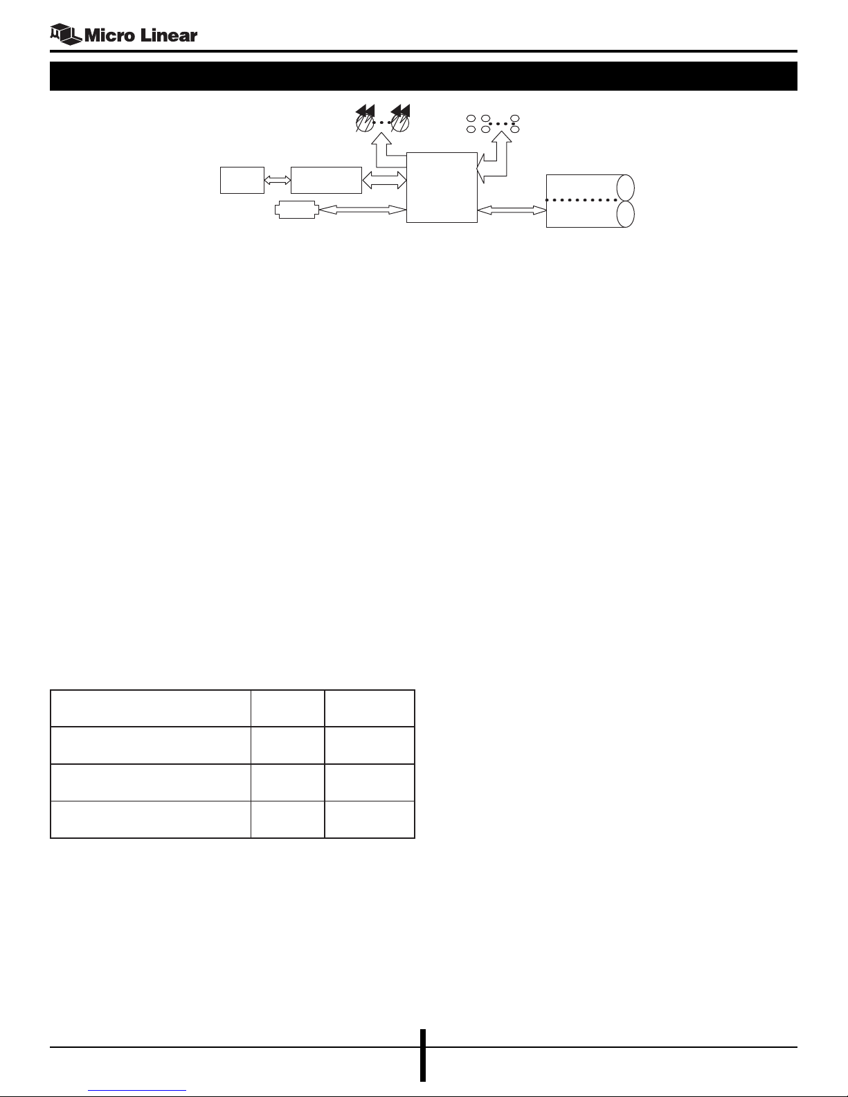
capabilities of the ML6651. The eval-board’s block diagram
is shown in Figure 1. This integrated circuit is a Media
Converter between twisted pair and fiber optic Ethernet
technologies. It supports conversion between 10BASE-T
and 10BASE-FL, between 100BASE-TX and 100BASE-FX/SX
and, between FLP Bursts and FLNP Bursts. (FLP: Fast Link
Pulse, FLNP: Fiber Link Negotiation Pulse.) One or both of
the fiber optic or twisted pair interfaces can be configured
to interface with industry standard 1x9 fiber optic PMD
modules, (using the PECL compatible modes) or minature
fiber optic comonents (typically called “sugar-cubes”) as it
supports both 850nm and 1300nm optics.
Three of the many possible configurations of the ML6651
eval boards are offered:
1) 10/100Mbs copper to 850/1300nm fiber optic “sugar
cubes”. This configuration has two board sizes: full
(rev. B), and mini (rev. E). See attached schematic
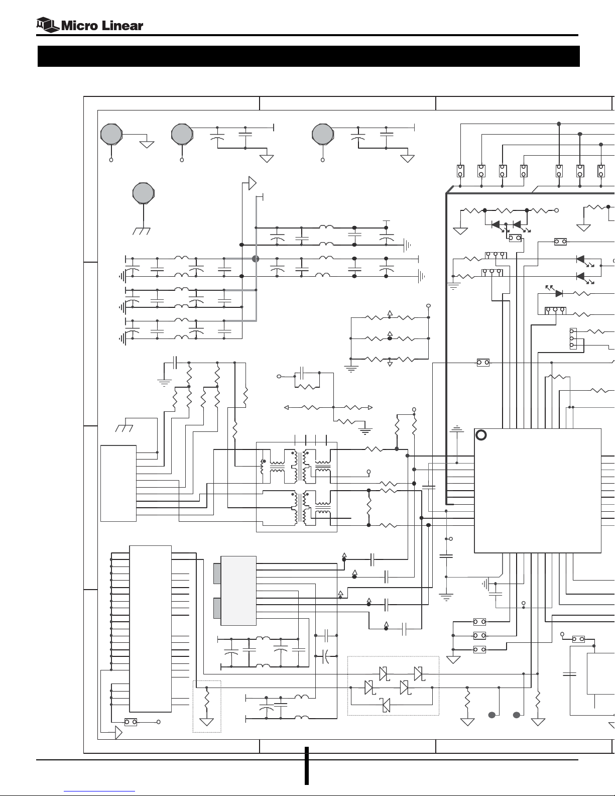
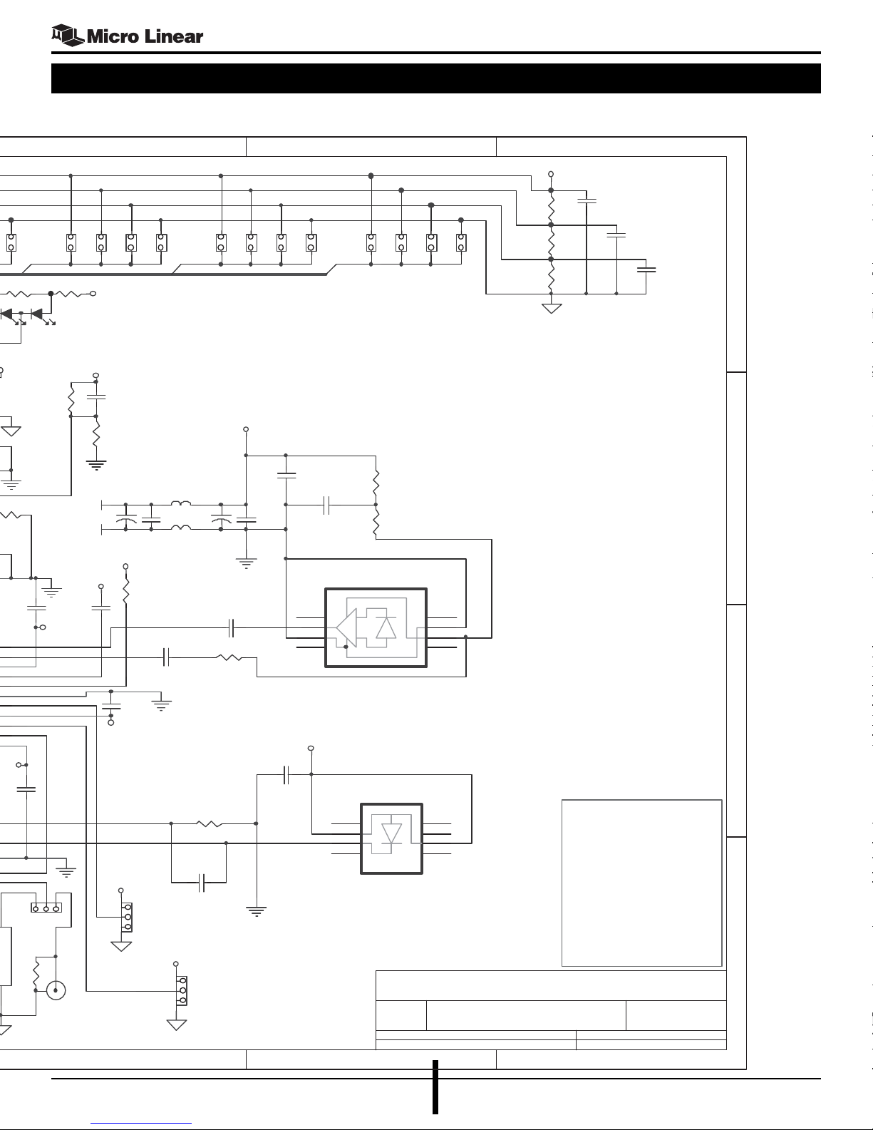
(Appendix D) labeled “ML6651 EVAL BOARD
SCHEMATIC (sugar cubes on right)”. The reduced or
mini size has layout and options restricted. But, it
comes with an AC-DC adapter since it has a 5V-to-
3.3V regulator on board. In contrast, the full size
version requires +5 and +3.3VDC supplies.
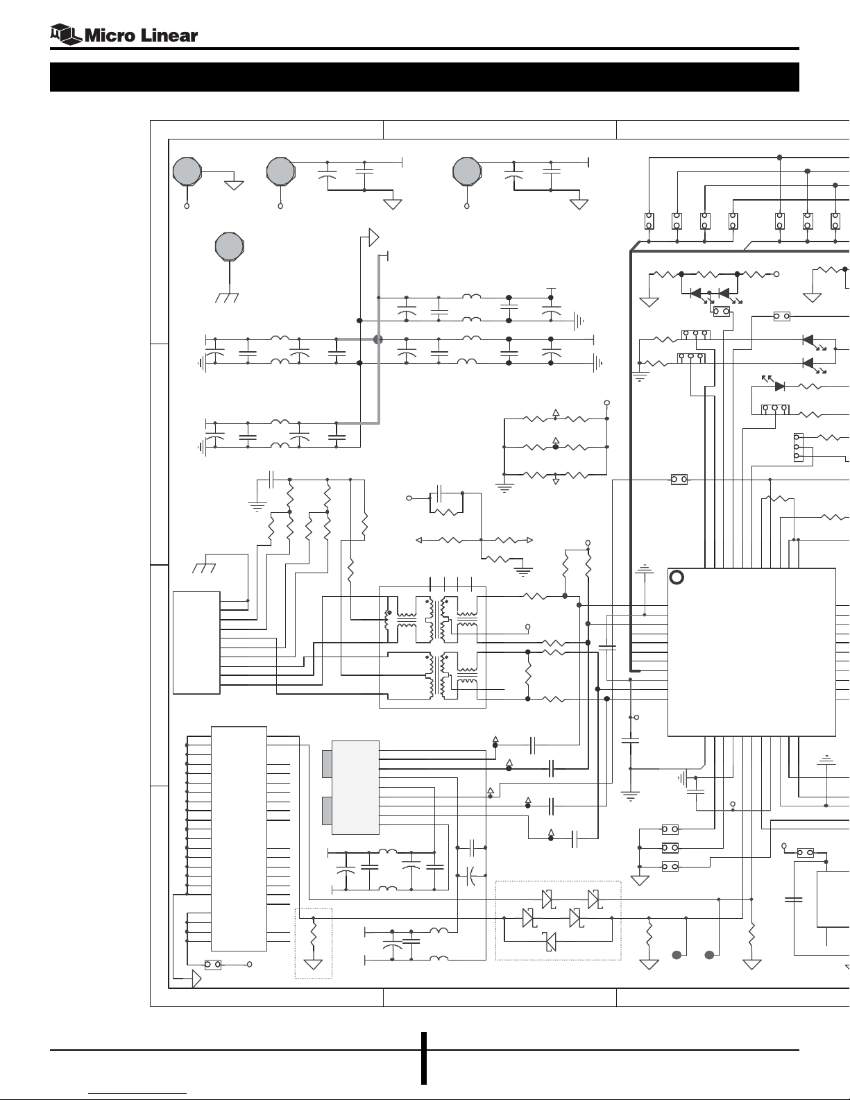
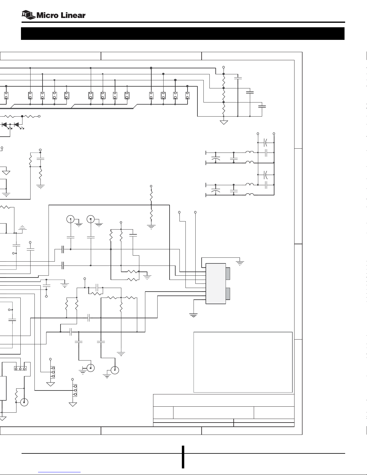
2) 10/100Mbs copper to 1300nm, 1X9 PECL module. See
attached schematic (Appendix B) labeled “ML6651
EVAL BOARD SCHEMATIC (9 pin module on right),
rev- A “. This full size board requires +5 and +3.3VDC
supplies and includes options for user defined
configuration purposes.
FEATURES
• Compatible with new TIA/EIA-785 10/100BASE-SX
standard. It is also intended to support ISO/IEC 8802.3
and IEEE 802.3 standards.
• Automatic detection and configuration of link for 10 or
100 Mbps operation using Auto-Negotiation protocol
(Transparent Mode)
• Supports Parallel Detection for speed configuration in
absence of FLP Bursts (Forced Mode)
• Supports SPEED and DUPLEX mode configuration in
absence of auto negotiation capability on fiber side
• Offers bandwidth migration from 10 Mbps to 100 Mbps
over fiber and copper networks
• Supports both miniature “sugar-cube” fiber-optic
components and PMD transceivers such as 1x9 (5V) or
MT-RJ (3.3V) PECL modules
• Multiple modes of operation for all network
configurations, especially Transparent Mode (see
ML6651 datasheet for more details)
• Transmission distance from 300 meters of multimode
fiber-optic cable up to 2 kilometers of singlemode fiber
optic cable
• Use 1:1 transformer ratio for TP’s transmit and receive
paths without requiring external filtering
• Integrated 100BASE-TX equalizer and baseline wander
correction circuits
3) 10/100Mbs copper to 1300nm, MT-RJ, PECL module.
See attached schematic (Appendix C) labeled
“ML6651 EVAL BOARD SCHEMATIC (MT-RJ on right),
rev-CMT”. Board requires +5 and +3.3VDC supplies,
full size only. This board is actually contructed by
using rev. A 1x9 PECL board above with different PCB
stuffing requirements. A daughter card is installed in
place of the 1X9 module. The daughter card carries the
MTRJ module and appropriate by-pass capacitors. The
schematic has reflected all the necessary changes:
epyT
eziS/veR
ebuCraguSLCEP9X1JRTM
lluF/B
iniM/E
lluF/A
iniM/*
• Integrated fiber optic receive quantizer
• Control logic for power-down, TP’s transmitter off, and
fiber optic transmitter off
• Single chip, low power, small footprint SMT
components: small PCB board
lluF/TMC
November 2001 User’s Guide
Page 2
ML6651
TABLE OF CONTENTS
Overview ....................................................................................................................................................................1
Features .......................................................................................................................................................................1
Disclaimer ...................................................................................................................................................................2
General Description.....................................................................................................................................................3
Evaluation Kit Contents ............................................................................................................................................................................................ 3
Theory of Operation ................................................................................................................................................................................................. 3
Testing .........................................................................................................................................................................6
Appendix A: Full Size Board with Sugar Cubes ...........................................................................................................7
Appendix B: Full Size Board with 1x9 Module.......................................................................................................... 15
Appendix C: Full Size Board Rev. CMT with MT-RJ Module......................................................................................22
Appendix D: Mini Size Board with Sugar Cubes ....................................................................................................... 27
DISCLAIMER
© 2001 Micro Linear Corporation. All rights reserved. All other trademarks are the property of their respective owners.
Products described herein may be covered by one or more of the following U.S. patents: 4,897,611;
4,964,026; 5,027,116; 5,281,862; 5,283,483; 5,418,502; 5,508,570; 5,510,727; 5,523,940; 5,546,017;
5,559,470; 5,565,761; 5,592,128; 5,594,376; 5,652,479; 5,661,427; 5,663,874; 5,672,959; 5,689,167;
5,714,897; 5,717,798; 5,742,151; 5,747,977; 5,754,012; 5,757,174; 5,767,653; 5,777,514; 5,793,168;
5,798,635; 5,804,950; 5,808,455; 5,811,999; 5,818,207; 5,818,669; 5,825,165; 5,825,223; 5,838,723;
5.844,378; 5,844,941. Japan: 2,598,946; 2,619,299; 2,704,176; 2,821,714. Other patents are pending.
Micro Linear makes no representations or warranties with respect to the accuracy, utility, or completeness
of the contents of this publication and reserves the right to make changes to specifications and product
descriptions at any time without notice. No license, express or implied, by estoppel or otherwise, to any
patents or other intellectual property rights is granted by this document. The circuits contained in this
document are offered as possible applications only. Particular uses or applications may invalidate some
of the specifications and/or product descriptions contained herein. The customer is urged to perform its
own engineering review before deciding on a particular application. Micro Linear assumes no liability
whatsoever, and disclaims any express or implied warranty, relating to sale and/or use of Micro Linear
products including liability or warranties relating to merchantability, fitness for a particular purpose, or
infringement of any intellectual property right. Micro Linear products are not designed for use in medical,
life saving, or life sustaining applications.
Headquarters: 2050 Concourse Drive, San Jose, CA 95131 (408) 433-5200 www.microlinear.com
WESTERN UNITED STATES
Micro Linear Corporation
2050 Concourse Drive
San Jose, CA 95131
Tel: (408) 433-5200
Fax: (408) 432-1627
CENTRAL UNITED STATES
Micro Linear Corporation
59 Cardinal Street
Pearl River, NY 10965
Tel: (845) 735-5848
Fax: (845) 735-5852
EASTERN UNITED STATES
Micro Linear Corporation
35 Pinehurst Avenue
Nashua, NH 03062
Tel: (603) 888-1326
Fax: (603) 888-4239
Micro Linear Corporation
EUROPE
102 Lesbourne Road
Reigate Surrey RH2 7JX England
Tel: +44 1737 224599
Fax: +44 1737 224599
2
Micro Linear Corporation
ASIA
Room D, 28/F., Block 8
1 Tsun King Road
Shatin, N.T., Hong Kong
Tel: 852-26348585
Fax: 852-27758284
November 2001User’s Guide
Micro Linear Corporation
JAPAN
1-17-8 Hasegawa Building
Hamamatsu-cho
Minato-ku, Tokyo 105-0013
Tel: 03-3438-1651
UG09-03
Page 3
GENERAL DESCRIPTION
ML6651
LEDS
RJ45 MAGNETIC
MII CONN
Figure 1. Basic ML6651 Evaluation Board Functional Block Diagram
EVALUATION KIT CONTENTS
The ML6651 Evaluation Kit contains the following items:
1. ML6651 Evaluation Kit Users Guide
2. ML6651 Evaluation Board with IC (ML6651)
3. ML6651 Data Sheets: please download the latest
revision from Micro Linear’s web site at
http:\\www.microlinear.com
THEORY OF OPERATION
JUMPERS
ML6651
FIBER OPTIC
XCVR or
SUGAR
CUBES
1. The ML6651 Evaluation Board is ideally suited to
operate in Transparent mode. In this mode, the ML6651
will optimally and automatically configure for Ethernet
technology, depending on the capabilities of the system
link partners. This is the “plug-and-play” mode if there
is a common denominator between the two link
partners. This is also the default configuration of board
shipped.
2. For a complete discussion of the various modes,
Transparent, Non Transparent, and Forced, see the
ML6651 Datasheet.
Modes of Operation
To meet the needs of all network configurations the full size
version of the ML6651 Evaluation Board may be configured
to any of the following 3 modes of operation using the two
jumpers labeled SPEED and DUPLEX (Note: These modes
can also be set via Serial Management Interface (SMI)
register #30):
EDOM)81J(DEEPS)71J(XELPUD
)deppihs.gifnoctluafed(tnerapsnarTtaolF
tnerapsnarT-noNtaolFdexiF
decroFdexiF
)1(
)2(
)1(
taolF
)2(
eraCt’noD
Table 2. Serial Management Interface Modes
(1)
Float = no jumper installed, default to VCC/2. Logically,
it means Auto-Negotiable.
(2)
Fixed = short to VCC or GND electrically. Logically, for
SPEED it means J18 forces 100Mbs or 10Mbs mode. For
DUPLEX, it means J17 forces FULL or HALF DUPLEX Mode.
Please see data sheets and attached schematics for more
details.
November 2001 User’s Guide
3
Page 4
GENERAL DESCRIPTION
ML6651
Media Selections
The ML6651 has two interfaces to different media. One
interfaces only to fiber optic link. The other can interface to
either fiber optic link or copper link. The jumper locations
labeled PECL_QU and PECL_TP help to set the
configurations (can also be set via MII register #30). For the
mini size boards, the configuration is fixed so these jumpers
are not available.
PT_LCEP
)3(
CCVforotcaf(
)
0
3/1
3/2
1
UQ_LCEP
)CCVforotcaf(
0
3/1
3/2
1
(3)
VCC = 3.3V nominal.
trohS
srepmuJ
13J
,12J,41J
92J
31J
4J
srepmuJtrohS
23J
92J,61J
51J
5J
taecafretnI
dna,-/+nipT
-/+tuopT
riaPdetsiwT
LCEPVL/LCEPsecarTBCP
riaPdetsiwTsecarTBCP
riaPdetsiwTm01
taecafretnI
dna,-/+nioF
)tuoI(toN/tuoI
dnarezitnauQ
revirdDEL
)mn058(
LCEPVL/LCEPsecarTBCP
dnarezitnauQ
revirdDEL
)mn0031(
dnarezitnauQ
revirdDEL
)mn0031/mn058(
kniLreppoC
htgneL
XT-ESAB001
dradnatS
kniLcitpOrebiF
)xam(htgneL
ESAB001/ESAB01
,mn0031,m003
mn058ro
mK2/mK2
m003/m003
Examples:
1. Full-length (100m) 10/100Mbs copper to 850nm/1300nm
miniature “sugar-cube” fiber optic components with
maximum fiber length of 2km: short J31 and J32
2. Full-length (100m) 10/100Mbs copper to PECL (1X9 pin
or MT-RJ module): short J31, J16, and J29
Status LEDs
Each of the media interfaces (TP or twisted-pair and FO or
fiber optic) has a set of three LEDs to indicate:
1) Data or Auto-Neg activities (D8, 9, RED)
2) Link speed is 10Mbs (D6, 7, YELLOW)
J26 is shorted to the FOAN_DT position, when not in TEST
mode.
J27 is shorted to the TPAN_DT position, not TEST.
J33-34 (FOINSPD, TPINSPD) must be shorted, also.
Do not change these settings.
Note: The mini size board will not have these jumpers, but
the LEDs are still available.
Miscellaneous
• J6, J25 (REFCLK): the ML6651 requires a 25MHz clock
source. J6 allows the board to select the on-board clock
oscillator (XTAL) at U4 or an alternate source. The
default position is on-board (XTAL). No jumper selection
for mini size boards.
• J28 (BCKPLINK): the ML6651 can enable a backup link
when the primary one is down when it is in Forced100Mbs non-loopback mode. RED LED (BCKLINK) at
D10 will be lit. Please refer to data sheet for more
information. J28 is normally not installed for full size
board. It is installed for mini boards between pin #2,
and #3 to disable the feature.
• J29 (SDTH): installed if PECL module is used. No
jumper selection for mini size board.
• J23 (FOOUTOFF#): shorted to disable fiber optic driver.
Normally, it is not installed.
• J24 (TPOUTOFF#): shorted to disable twisted pair driver.
Normally, it is not installed.
• J35 (PWRDWN#): shorted to power down the ML6651.
Normally, it is not installed.
• J21 (PMD) : installed if PECL is selected instead of
Twisted-pair, (i.e., fiber to fiber conversion).
• J22 (MII power): If +5VDC is supplied through the MII
connector then this jumper must be shorted. Normally, it
is not installed since power is supplied via banana jacks
labeled +3.3V, +5V, and GND. No jumper selection for
mini size board.
• MII connector: allows optional access to a limited and
proprietary-defined set of registers, not available for mini
size board.
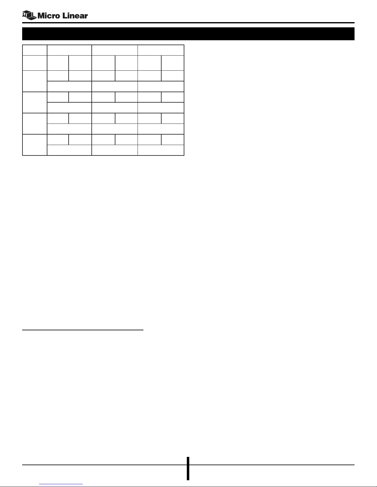
• PHY address jumpers: whenever the MII connector is
available, the proprietary MII registers can be accessed
via any one of the PHY address from 0 to 31 (decimal)
by setting up jumpers labeled AD10, AD32, and
AD4_LIW as follows: (short the corresponding jumpers
to achieve desired setting)
3) Link speed is 100Mbs (D11, 12, GREEN)
4
November 2001User’s Guide
Page 5
GENERAL DESCRIPTION
ML6651
emaNniP”WIL_4DA“”23DA“”01DA“
forotcaf(
)CCV
0
3/1
3/2
1
)4(
WIL
elbasiD 00000
elbanE01010
elbanE 11111
elbasiD10101
YHP
noitcnuf
03J02J91J
01J8J21J
9J7J11J
2J1J3J
YHP
tib4#DA
YHP
tib3#DA
tib2#DA
YHP
YHP
tib1#DA
(4) Please refer to data sheet for description of LIW function
in the Pin Descriptions section. The shipped configuration is
“Disable”.
Examples:
a) PHY address = 1, no LIW —> short J3, J20, J30.
b) PHY address = 1 plus LIW —> short J3, J20, J10.
Board is typically shipped as (a).
• SMA connectors: optional for external OSC, and optical
Tx/Rx signals (TD+/-, RD+/-), or for testing purposes.
Note: Not available for mini size board.
• Banana power jacks for +3.3V, +5V, and GND, not
available for mini size board which comes with AC to
+5VDC adapter and on-board 3.3V regulator.
Note: Always refer to schematic and data sheet for more details.
In summary, typical jumpers installed for each board are
shown below:
BOARD EVALUATION
Make sure the power is off when making electrical
tib0#DA
connections. The operators should be grounded before
touching the board to minimize the threat of Electro Static
Discharge (ESD). Power is applied after all the connections
have been made. Normal operation and initialization
process begins at power up.
The following items are useful for testing and evaluating the
ML6651 Evaluation Board:
• Either of the two most popular optical fiber cable sizes,
50/125 micron or 62.5/125 micron multi mode fiber
cable can be used as the fiber link
• Fiber optic power meters (850/1300nm wave length)
such as the Fotec Power meter
• Fiber optic attenuators
• An optical to electrical converter. Micro Linear uses
the BCP waveform receiver model 300
• Network Interface Cards (NIC’s) or Netcom’s Fast
Ethernet (Smart Bits 2000) testers
• Twisted-pair cables of various lengths (100m Ethernet
Standard: max 100m) with crossover wiring
• The jumpers are installed as pre-configured
Rev. Jumpers #
A, CMT 6,16,19,20,25-27,30,33,34
B 3,5,6,20,25-27,30,31,33,34
E28
Note: The jumpers for PHY address are either configured for ADDRESS 0 or 1,
typically. Please refer to previous tables.
November 2001 User’s Guide
5
Page 6
GENERAL DESCRIPTION
ML6651
TESTING
Install the twisted pair and fiber cables. Use the attenuators
in the fiber links if desired. The board’s RJ45 jack has a
straight or NIC wiring so be sure to use a crossover copper
cable or a separate crossover adapter.
The normal mode of operation is Transparent Mode, or plugand-play mode, if a common denominator is found between
the two copper end ports.
The plug and play mode is as follows:
Connect the power source and turn it on. LEDs should start
to blink and finally are settled to either the 10Mbs or
100Mbs LEDs, whichever is the common speed (must be a
pair). It may take a few cycles with LEDs running up and
down if Auto-negotiation is taking place. If the AN_DT LEDs
keeps blinking or only one of the speed LED is ON instead
of a pair (both 10 or both 100), then no link has been
established. Recheck the configurations of your copper
stations and reconfigure the eval-board if needed (to NonTransparent or Fixed mode).
If one of the TP link partner’s capabilities is changed, autonegotiation may be restarted automatically by disconnecting
and reconnecting the cables. Alternatively, auto-negotiation
may be restarted from the Netcom’s SmartBits 2000 software
graphical interface. If no common operating mode is found
between two link partners the red (D8, D9 LED(s) will
remain flashing for the auto-negotiation capable link
partner(s) as long as FLP and FLNP bursts are received.
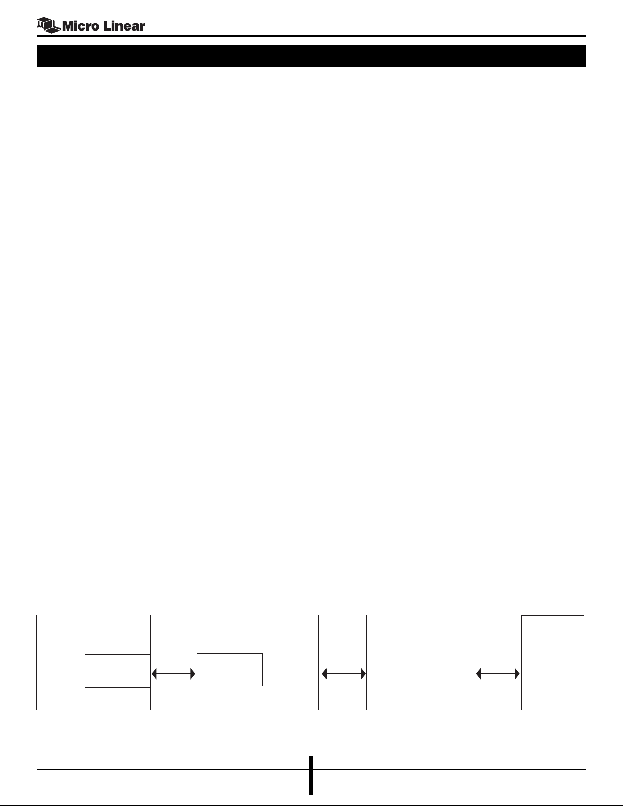
One way to test the ML6651 Evaluation Board is shown in
Figure 4. The Netcom SmartBit 2000 system can have its
port configured to look like a legacy or auto-negotiable
station. The configuration of the ML6651 eval board can be
changed accordingly. Once link is established, data (with
variable lengths and patterns) can be transferred from one
Netcom port and received at another.
To measure the launch power at the transmitter, disconnect
the fiber optic cable from the optical receiver module and
connect it to the power meter. Measure the power while the
pattern generator is transmitting. Note that the reading of the
power meter applies to the average launch power: Average
launch power (dBm) = peak launch power (dBm) minus
3dBm
To measure optical rise and fall time connect the fiber optic
cable from the optical transmitter to the optical waveform
receiver and then to the scope. You need to program the
data to a specific pattern like AAhex (not random).
To measure optical sensitivity use the variable attenuator to
attenuate the power. Start to transmit a random pattern and
then observe that the Link LED stays on. Then attenuate the
optical signal during transmission until the Link LED goes
off. Now slightly increase the optical signal through the
attenuator to turn the Link LED back on. Finally measure
the receive power by the power meter to find the receive
sensitivity.
Evaluation Board Errata
This applys to all four board configurations to avoid
confusion. Do not stuff C49 & C50 located upper right
corner of schematics on full size boards and top center on
the mini board. For a complete discussion of the use of the
control & configuration pins, see the ML6651 datasheet
section Configuration and Control Options and Guidelines.
NIC or
HUB or
Switch or
Netcom SmartBits 2000
RJ45
FLPs FNLPs
ML6651Evaluation Board
6
Fiber
RJ45
Figure 2. Test Circuit Block Diagram
Optic
xcvr
November 2001User’s Guide
Other Media Converter
or Netcom SmartBits
2000 port with fiber
optical xcvr
FLPs
Other TP link
or Netcom
SmartBits
2000 TP
port if needed
Page 7
ML6651
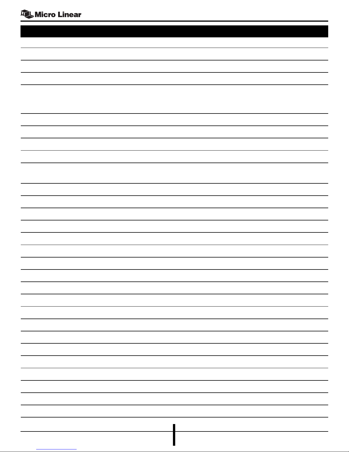
APPENDIX A: FULL-SIZE BOARD WITH SUGAR CUBES: BOM, SCHEMATIC, & ARTWORKS
Part Type Designator Quantity Manufacturer Part Number
ΩΩ
0
Ω, 0805 R23-26, 33 5 Digi-Key or equiv. P0.0ACT-ND
ΩΩ
0.001uF, 0805 C052 1 Digi-Key or equiv. PCC102BNCT-ND
0.01uF, 0805 C5,26,27,33 4 Digi-Key or equiv. PCC103BNCT-ND
0.1uF, 0805 C1-4,6,11-23,29,30,
32,34-36,41-43,48-51,1 35 Digi-Key or equiv. PCC1840CT-ND
50-152,157
0.47uF, 0805 C047 1 Digi-Key or equiv. PCC1818CT-ND
ΩΩ
1.4K
Ω 1%, 0805 R8,20,39,58,84 5 Digi-Key or equiv. P1.40KCCT-ND
ΩΩ
1/4 JACK JACK1-4 4 Digi-Key or equiv. J147-ND
ΩΩ
100
Ω 1%, 0805 R45 1 Digi-Key or equiv. P100ACT-ND
ΩΩ
10uF 20% Tant 16V, C7-10,24,25,31,
B size 37-40,44-46,153-156 18 Digi-Key or equiv. PCS3106CT-ND
ΩΩ
130
Ω 1%, 0805 R72-74 3 Digi-Key or equiv. P130ACT-ND
ΩΩ
ΩΩ
150
Ω 1%, 0805 R61,62,65,66 4 Digi-Key or equiv. P150ACT-ND
ΩΩ
ΩΩ
1K
Ω 1%, 0805 R46,86-89 5 Digi-Key or equiv. P1.0KACT-ND
ΩΩ
ΩΩ
20K
Ω 1%, 0805 R10-12 3 Digi-Key or equiv. P20KACT-ND
ΩΩ
ΩΩ
2K
Ω 1%, 0805 R07 1 Digi-Key or equiv. P2.0KACT-ND
ΩΩ
ΩΩ
30
Ω 1%, 0805 R32 1 Digi-Key or equiv. P30ACT-ND
ΩΩ
330pF 20%, 3KV, cer disc C028 1 Digi-Key or equiv. P4502A-ND
ΩΩ
4.02K
Ω 1%, 0805 R57,85 2 Digi-Key or equiv. P4.02KCCT-ND
ΩΩ
ΩΩ
475
Ω 1%, 0805 R60,75,76 3 Digi-Key or equiv. P475CCT-ND
ΩΩ
ΩΩ
5
Ω 1%, 0805 R47-48 2 Digi-Key or equiv. P5.1ACT-ND
ΩΩ
ΩΩ
49.9
Ω 1%, 0805 R1-2,22,49-54 9 Digi-Key or equiv. P49.9CCT-ND
ΩΩ
ΩΩ
511
Ω 1%, 0805 R67-68 2 Digi-Key or equiv. P511CCT-ND
ΩΩ
ΩΩ
5K
Ω 1%, 0805 R09-21 2 Digi-Key or equiv. P4.99KCCT-ND
ΩΩ
ΩΩ
75
Ω 1%,0805 R55,56 2 Digi-Key or equiv. P75ACT-ND
ΩΩ
ΩΩ
82
Ω 1% R81-83 3 Digi-Key or equiv. P82ACT-ND
ΩΩ
Diode, SOD123 D1-5 SOD123 Digi-Key or equiv. SD101-CWDICT-ND
Ferrite Bead, 1812 L1-6,10-19 16 Digi-Key or equiv. P9812CT-ND
JUMPER 2 PIN J1-5,7-16,19-25,30-35 35 Digi-Key or equiv. WM4000-ND
JUMPER 3 PIN J6,17-18,26-29 7 Digi-Key or equiv. WM4001-ND
November 2001 User’s Guide
7
Page 8
ML6651
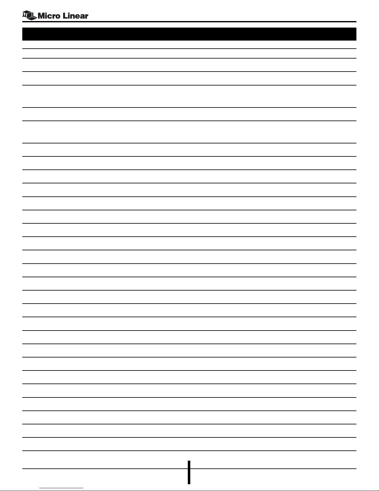
APPENDIX A: FULL-SIZE BOARD WITH SUGAR CUBES: BOM, SCHEMATIC, & ARTWORKS
Part Type Designator Quantity Manufacturer Part Number
LED (green) D11,12 2 Digi-Key or equiv. L20665-ND
LED (red) D8-10 3 Digi-Key or equiv. L20661-ND
LED (yellow) D6,7 Chassis 2 Part of 36 pin Header
MII-CONN 40 PIN, P01 1 Lo Dan West (650) 592-4600 FCN238P040GF
Male, Edge Mount
Oscillator 25MHz U4 1 Digi-Key or equiv. SE2837CT-ND (SG636)
RJ45-SHIELDED receptacle, T1 1 any
8-pin modular
SMA Conn. SMA1 1 Digi-Key or equiv. J502-ND
Test Pin 3.3V Test Pin Part of 36 pin Header XXXXXXXXXXXX
Test Pin 5V Test Pin Part of 36 pin Header XXXXXXXXXXXX
Test Pin Chassis 2 Part of 36 pin Header XXXXXXXXXXXX
Test Pin DGnd 6 Part of 36 pin Header XXXXXXXXXXXX
Test Pin GNDBQ Test Pin Part of 36 pin Header XXXXXXXXXXXX
Test Pin GNDE Test Pin Part of 36 pin Header XXXXXXXXXXXX
Test Pin GNDFC Test Pin Part of 36 pin Header XXXXXXXXXXXX
Test Pin GNDL Test Pin Part of 36 pin Header XXXXXXXXXXXX
Test Pin GNDRX1 Test Pin Part of 36 pin Header XXXXXXXXXXXX
Test Pin GNDRX2 Test Pin Part of 36 pin Header XXXXXXXXXXXX
Test Pin GNDT Test Pin Part of 36 pin Header XXXXXXXXXXXX
Test Pin GNDTX1 Test Pin Part of 36 pin Header XXXXXXXXXXXX
Test Pin M10 Test Pin Part of 36 pin Header XXXXXXXXXXXX
Test Pin MDC Test Pin Part of 36 pin Header XXXXXXXXXXXX
Test Pin VCC3D Test Pin Part of 36 pin Header XXXXXXXXXXXX
Test Pin VCCBQ Test Pin Part of 36 pin Header XXXXXXXXXXXX
Test Pin VCCE Test Pin Part of 36 pin Header XXXXXXXXXXXX
Test Pin VCCFC Test Pin Part of 36 pin Header XXXXXXXXXXXX
Test Pin VCCL Test Pin Part of 36 pin Header XXXXXXXXXXXX
Test Pin VCCRX1 Test Pin Part of 36 pin Header XXXXXXXXXXXX
Test Pin VCCRX2 Test Pin Part of 36 pin Header XXXXXXXXXXXX
Test Pin VCCT Test Pin Part of 36 pin Header XXXXXXXXXXXX
8
November 2001User’s Guide
Page 9

ML6651
APPENDIX A: FULL-SIZE BOARD WITH SUGAR CUBES: BOM, SCHEMATIC, & ARTWORKS
Part Type Designator Quantity Manufacturer Part Number
Test Pin VCCTX1 Test Pin Part of 36 pin Header XXXXXXXXXXXX
Test Pins All Test Pins 36 pin header Digi-Key or equiv. S1212-36-ND
10/100 Magnetic T2 1 PULSE H1019
10/100BASE-SX U1 1 Micro Linear ML6651
media converter
Fiber optic LED U2 1 Agilent HFBR-1312T
transmitter (1300nm), or HFBR-
1414T (850nm)
Fiber optic PIN U3 1 Agilent HFBR-2316T
preamp rcvr (1300nm), HFBR-2416T
(850nm)
Bare PCB Rev B 1 Micro Linear
November 2001 User’s Guide
9
Page 10
ML6651
2
2
OUT
3
GND
2
C
APPENDIX A: FULL-SIZE BOARD WITH SUGAR CUBES: BOM, SCHEMATIC, & ARTWORKS
321
JACK2
DGND IN
D
GNDFC
GNDL
GNDT
C
B
RJ45-SHIELDED
A
BANANA
VCCFC
VCCL
VCCT
Chassis GND
SHLD
SHLD
T1
RXTP-
RXTP+
TXTP-
TXTP+
22
23
24
25
26
27
28
29
30
31
32
33
34
35
36
37
38
39
1
20
21
40
VCCMII
DGND
DGND
JACK3
BANANA
Chassis GND (earth)
+
C44
10uF
+
C45
10uF
+
C24
10uF
330pF, 3KV
GNDT
10
9
8
NC
7
NC
6
5
NC
4
NC
3
2
1
MII-CONN
MDIO
GND
MDC
GND
GND
GND
RXD3
RXD2
GND
RXD1
GND
RXD0
GND
RXDV
GND
RXCK
GND
RXER
GND
GND
GND
GND
TXER
TXCK
GND
TXEN
GND
TXD0
GND
TXD1
GND
TXD2
GND
TXD3
VCC
VCC
COL
VCC
VCC
J22
JACK4
C37
+
C153
10uF
+
C155
10uF
+
C9
10uF
VCC5D
10uF
DGND
See Note 1
R21
5K
DGND
TX
RX
C8
10uF
C157
0.1
C152
0.1
C13
0.1
50
50
OPMOD1
VCC5D
DGND
DGND
R55
75
11
10
TXGND
OPOUTP
OPOUTN
VCCTX
VCCRX
OPINN
OPINP
RXGND
C6
BANANA
+3.3v DIGITAL IN
L16
C42
L15
0.1
L18
C43
L17
0.1
L19
C4
L14
0.1
C28
R5350R54
R4950R5050R5150R52
P1
2
3
4
5
6
7
8
9
10
11
12
13
14
15
16
17
18
19
CRS
VCC5D
1 2 3
R56
75
8
6
7
9
SD
C5
.01
0.1
10uF
VCC3D
VCCTX1
T2
RX+
9
8
7
6
5
4
3
2
1
L3
C40
10uF
L2
C7
VCC3D
DGND
TX+
+
C156
10uF
+
C10
10uF
R84
<-----N/C----->
13 12 5 4
C21
L4
C1
0.1
+5v DIGITAL IN
L13
C157
L10
0.1
L11
C14
L12
0.1
C51
0.1
1.4K
R75
475
1:1
0.1
10uF
L1
JACK1
BANANA
C20
0.1
C39
C29
.1
GNDRX1
R76
4.02K
GNDTX1
1
3
2
16
14
15
VTX1+
VSD1
C25
10uF
C15
0.1
R72
130
R73
130
R74
130
475
R85
0
VCCT
R45
100
N/C
VTX1-
VRX1-
D2
D3 D4
VCCBQ
+
+
VRX1+
VRX1-
VSD1
VTX1-VTX1+
R1
51
R23
0
0
C23
0.1
C2
0.1
VRX1+
See Note 1
D5
R240
R25
R26
C33
.01
C46
C31
10uF
C22
0.1
10uF
R81
82
R82
82
R83
82
VCCT
C3
0.1
D1
VCC5D
DGND
GNDBQ
VCCE
GNDE
VCCRX1
R2
51
C41
0.1
J3 J11 J12
AD10
R65
150
DGND
R87 1K
R86
1K
GNDT
GNDT
1
2
3
4
5
6
7
8
9
10
11
VCCE
C12
0.1
DGND
GNDE
DGND
DGND
J21
SD
TPOUTP
GNDT
TPOUTN
AD4_LIW
AD32
AD10
PECL_TP
PECL_QU
VCCE
TPINP
TPINN
C11
0.1
J24
J23
J35
R20
1.4K
D11
TEST
1
TP1
1
J26
AD32
39
40
41
SDTH
TPINSPD
BCKPLINK
ML6651
GNDD
MDIO16MDC17REFCLK
15
J1 J7 J8
R61
VCC3D
150
J34
D8
D9
D10
1
J28
1
J29
R7
2K
35
36
37
38
RTTP
RTOP
GNDB
REQ_SD
VCCD19GNDL
IOUT21IOUT
18
20
VCC3D
C16
0.1
R39
1.4K
DGND
R60
475
R88
1K
34
GNDQ
PWRDWN#
22
J25
J19 J
R67
511
D6
J33
J27
42
43
44
FOINSPD
TPAN_DT
FOAN_DT
44 PIN TQFP
GNDE
TPOUTOFF#
FOOUTOFF#
12
13
14
VCC3D
TP2
TEST
R66
150
DGND
R89
1K
FOINP
FOINN
VCCQ
CQOS
SDFO
GNDFC
SPEED
VCCFC
DUPLEX
VCCL
4
1
R8
VCC
N/C
D1
VC
R9
1.4K
Oscillator
3
3
3
3
2
2
2
2
2
2
2
V
10
November 2001User’s Guide
Page 11
APPENDIX A: FULL-SIZE BOARD WITH SUGAR CUBES: BOM, SCHEMATIC, & ARTWORKS
OUT
3
GND
2
AD4_LIW
D7
DGND
J2 J9 J10
R62
150
VCCRX2
R58
1.4K
VCC3D
C36
0.1
R57
4.02K
0 J30 J31 J32
R68
511
J4 J13 J14
PECL_TP
J5 J15 J16
PECL_QU
VCCRX2
VCC3D
R10
20K
R11
20K
R12
20K
DGND
C48
0.1
ML6651
654
C49
0.1
C50
0.1
D
3
2
1
0
9
8
7
6
5
4
3
CL
DGND
GNDBQ
5K
U4
25MHz
R22
49.9
GNDBQ
C18
0.1
VCCBQ
C35
0.1
GNDL
J6
1
ExtClkin
(edge-mount SMA)
VCC5D
DGND
C30
0.1
+
GNDRX2
.01
30
C17
0.1
C19
0.1
(PLACE BYPASS CAPS CLOSE TO F/O MODULES)
GNDL
C47
0.47
Fiber Optic Receiver
U3
1
N/C
2
3
4
N/C N/C
VCCL
C34
0.1
N/C
R48
5.0
R47
5.0
VCC
VEE
Fiber Optic Transmitter
U2
Anode
1
2
3
4
Cathode
Title
ML6651 EVAL BOARD SCHEMATIC (sugar cubes on right)
Date:
File:
B
8
N/C
7
6
5
8
N/C
7
N/C
6
5
N/CN/C
Number RevisionSize
GNDRX2
C27
C151
0.1
.01
GNDFC
VCC3D
L6
L5
1
J17
DGND
C38
10uF
R46
C52
0.001uf
C26
R32
1K
+
C154
10uF
VCCFC
VCCBQ
R33
0
C32
0.1
VCCFC
VCC3D
1
J18
DGND
4 5 6
11 Planes on PCB, Digital: 5v & 3.3v.
Analog: 5v RX (sugar cube), 9 pin mod
needs 5v TX & RX, and the DUT needs
5 analog planes; T, E, L, FC & BQ.
RJ45 + half magnetics on isolated
& no inner planes.
TX sugar cube uses L (3.3v, analog)
for power.
Each plane has separate bead (vcc &
gnd) and filter caps. Digital Gnds
share same gnd plane.
NOTE 1: D1-5 & R21 may not be needed
B
C
B
A
November 2001 User’s Guide
11
Page 12
ML6651
APPENDIX A: FULL-SIZE BOARD WITH SUGAR CUBES: BOM, SCHEMATIC, & ARTWORKS
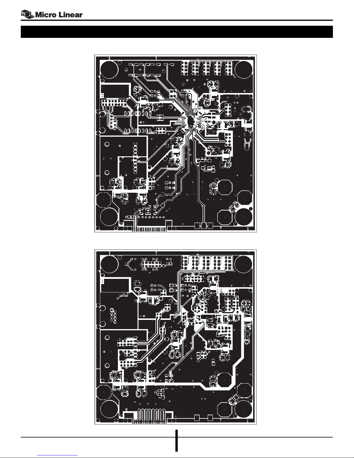
ML6651B Layer: Top
ML6651B Layer: Bottom
12
November 2001User’s Guide
Page 13
ML6651
APPENDIX A: FULL-SIZE BOARD WITH SUGAR CUBES: BOM, SCHEMATIC, & ARTWORKS
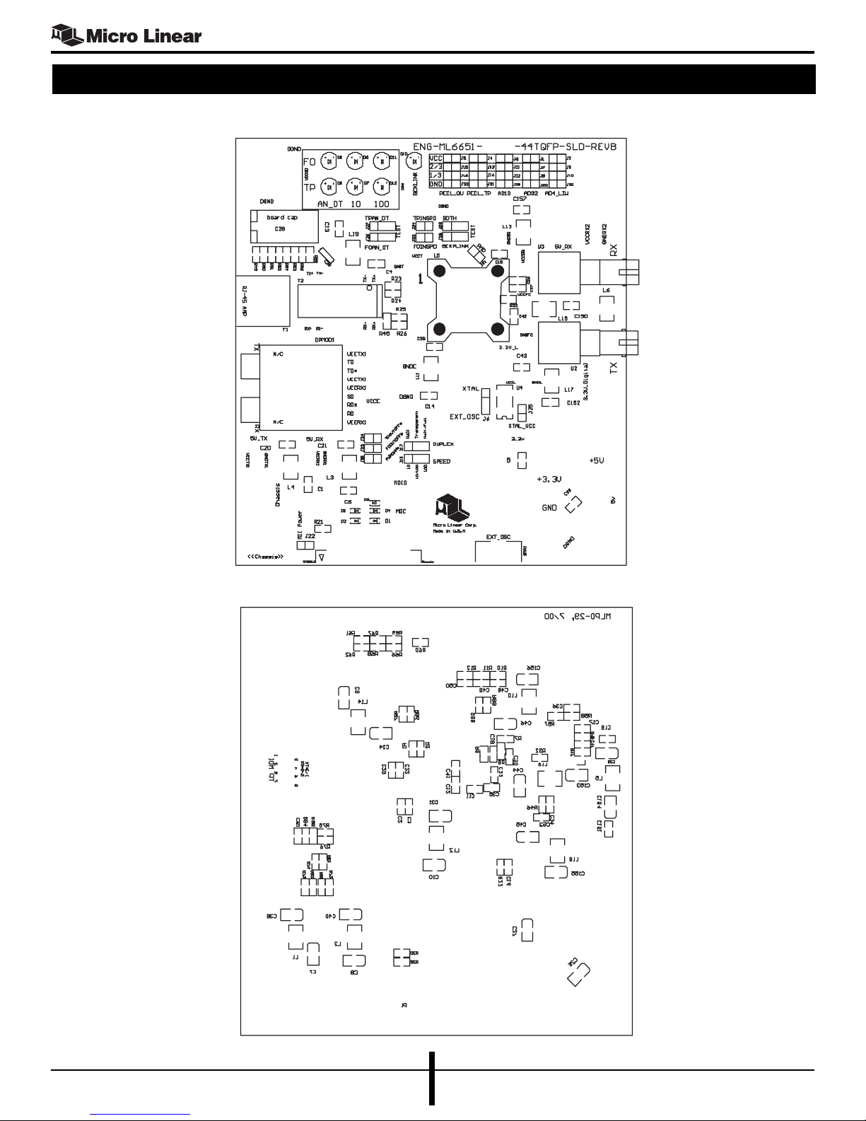
ML6651B Layer: Top Silk
ML6651B Layer: Bottom Silk
November 2001 User’s Guide
13
Page 14
ML6651
APPENDIX A: FULL-SIZE BOARD WITH SUGAR CUBES: BOM, SCHEMATIC, & ARTWORKS
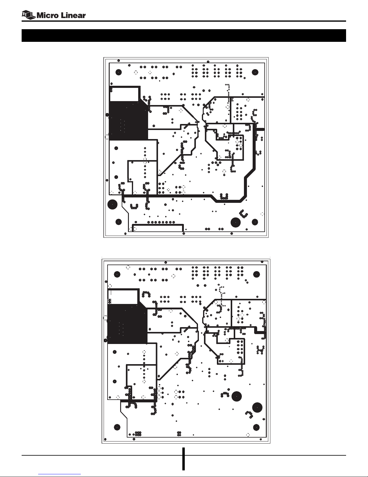
ML6651B Layer: VCC Plane
ML6651B Layear: Ground Plane
14
November 2001User’s Guide
Page 15
ML6651
APPENDIX B: FULL-SIZE BOARD WITH 1X9 MODULE: BOM, SCHEMATIC, & ARTWORKS
Part Type Designator Quantity Manufacturer Part Number
ΩΩ
0
Ω 1% 0805 R23-26 4 Digi-Key or equiv. P0.0ACT-ND
ΩΩ
µµ
0.01
µF 20% 0805 C5,33, 107-4, 108 4 Digi-Key or equiv. PCC103BNCT-ND
µµ
µµ
0.1
µF 20%, 0805 C1,4,6,8-16,20,21, 37 Digi-Key or equiv. PCC1840CT-ND
µµ
29,41,43,48-51, 101,102,
105,106,109,110,112-115,
157,201,202,206
ΩΩ
1.4K
Ω 1%, 0805 R08,20,39,58,84,103 6 Digi-Key or equiv. P1.40KCCT-ND
ΩΩ
1/4 JACK JACK1-4 4 Digi-Key or equiv. J147-ND
ΩΩ
100
Ω 1%, 0805 R45 1 Digi-Key or equiv. P100ACT-ND
ΩΩ
µµ
10
µF 20% Tant 16V, C7-10,24-25, 18 Digi-Key or equiv. PCS3106CT-ND
µµ
B size 31,32,37,39,40,45,103,104,
156,203,204,208
ΩΩ
130
Ω 1%, 0805 R28,72-74,106,108 6 Digi-Key or equiv. P130ACT-ND
ΩΩ
ΩΩ
150
Ω 1%, 0805 R61,62,65-66 4 Digi-Key or equiv. P150ACT-ND
ΩΩ
1K 1%, 0805 R86-89 4 Digi-Key or equiv. P745CCT-ND
ΩΩ
49.9
Ω 1%, 0805 R1-2,22,49-54 9 Digi-Key or equiv. P49.9CCT-ND
ΩΩ
ΩΩ
511
Ω 1%, 0805 R67,68 2 Digi-Key or equiv. P511CCT-ND
ΩΩ
ΩΩ
5K
Ω 1%, 0805 R9,21 2 Digi-Key or equiv. P4.99KCCT-ND
ΩΩ
ΩΩ
75
Ω 1%, 0805 R55,56,111,112 4 Digi-Key or equiv. P75ACT-ND
ΩΩ
ΩΩ
82
Ω 1%, 0805 R27,81-83,105,107 6 Digi-Key or equiv. P82ACT-ND
ΩΩ
Diode SOD123 D1-5 5 Digi-Key or equiv. SD101-CWDICT-ND
Ferrite Bead, 1812 L1-4,10-14,17-19,101-104 16 Digi-Key or equiv. P9812CT-ND
JUMPER 2 PIN J1-5,7-16,19-25,30-35 28 Digi-Key or equiv. WM4000-ND
JUMPER 3 PIN J6,17,18,26-29 7 Digi-Key or equiv. WM4001-ND
LED (green) D11,12 2 Digi-Key or equiv. L20665-ND
LED (red) D8,9 3 Digi-Key or equiv. L20661-ND
LED (yellow) D6,7 2 Digi-Key or equiv. L20667-ND
MII-CONN 40 PIN, male, P01 1 Lo Dan West (650) 592-4600 FCN238P040GF
edge mount
1x9 fiber optic transceiver OPMOD2 1 Agilent HFBR-5103
Oscillator 25MHz U4 1 Digi-Key or equiv. SE2837CT-ND (SG636)
November 2001 User’s Guide
15
Page 16
ML6651
APPENDIX B: FULL-SIZE BOARD WITH 1X9 MODULE: BOM, SCHEMATIC, & ARTWORKS
Part Type Designator Quantity Manufacturer Part Number
RJ45-SHIELDED receptacle, T1 1 Any
8-pin modular
SMA Conn. SMA1-5 5 Digi-Key or equiv. J502-ND
Test Pin 3.3V Test Pin Part of 36 pin Header XXXXXXXXXXXX
Test Pin 5V Test Pin Part of 36 pin Header XXXXXXXXXXXX
Test Pin Chassis 2 Part of 36 pin Header XXXXXXXXXXXX
Test Pin DGnd 6 Part of 36 pin Header XXXXXXXXXXXX
Test Pin GNDBQ Test Pin Part of 36 pin Header XXXXXXXXXXXX
Test Pin GNDE Test Pin Part of 36 pin Header XXXXXXXXXXXX
Test Pin GNDFC_L Test Pin Part of 36 pin Header XXXXXXXXXXXX
Test Pin GNDRX1 Test Pin Part of 36 pin Header XXXXXXXXXXXX
Test Pin GNDRX2 Test Pin Part of 36 pin Header XXXXXXXXXXXX
Test Pin GNDT Test Pin Part of 36 pin Header XXXXXXXXXXXX
Test Pin GNDTX1 Test Pin Part of 36 pin Header XXXXXXXXXXXX
Test Pin GNDTX2 Test Pin Part of 36 pin Header XXXXXXXXXXXX
Test Pin M10 Test Pin Part of 36 pin Header XXXXXXXXXXXX
Test Pin MDC Test Pin Part of 36 pin Header XXXXXXXXXXXX
Test Pin VCC3D Test Pin Part of 36 pin Header XXXXXXXXXXXX
Test Pin VCCBQ Test Pin Part of 36 pin Header XXXXXXXXXXXX
Test Pin VCCE Test Pin Part of 36 pin Header XXXXXXXXXXXX
Test Pin VCCFC_L Test Pin Part of 36 pin Header XXXXXXXXXXXX
Test Pin VCCRX1 Test Pin Part of 36 pin Header XXXXXXXXXXXX
Test Pin VCCRX2 Test Pin Part of 36 pin Header XXXXXXXXXXXX
Test Pin VCCT Test Pin Part of 36 pin Header XXXXXXXXXXXX
Test Pin VCCTX1 Test Pin Part of 36 pin Header XXXXXXXXXXXX
Test Pin VCCTX2 Test Pin Part of 36 pin Header XXXXXXXXXXXX
Test Pins All Test Pins 36 pin header Digi-Key or equiv. S1212-36-ND
10/100 Magnetic T2 1 PULSE H1019
10/100BASE-SX media converter U1 1 Micro Linear ML6651
Bare PCB Rev. A 1 Micro Linear
16
November 2001User’s Guide
Page 17
ML6651
November 2001 User’s Guide
17
Page 18
ML6651
1 2 3
321
D
C
B
A
TXTP+
1
TXTP-
2
RXTP+
3
NC
4
NC
5
RXTP-
6
NC
7
NC
8
SHLD
9
SHLD
10
T1
RJ45-SHIELDED
RXGND
1
OPINP
2
OPINN
3
SD
4
VCCRX
5
VCCTX
6
OPOUTN
7
OPOUTP
8
TXGND
9
RX
TX
OPMOD1
7
8
6
3
2
1
1:1
TX+
RX+
14
15
16
9
10
11
T2
R1
51
R2
51
VCCT
VCCT
R7
2K
R8
1.4K
R9
J1 J7 J8
AD32
J3 J11 J12
AD10
R23
0
R240
R45
100
C2
0.1
C3
0.1
R25
0
R26
0
VCC
1
MDIO
2
MDC
3
RXD3
4
RXD2
5
RXD1
6
RXD0
7
RXDV
8
RXCK
9
RXER
10
TXER
11
TXCK
12
TXEN
13
TXD0
14
TXD1
15
TXD2
16
TXD3
17
COL
18
CRS
19
VCC
20
VCC
21
GND
22
GND
23
GND
24
GND
25
GND
26
GND
27
GND
28
GND
29
GND
30
GND
31
GND
32
GND
33
GND
34
GND
35
GND
36
GND
37
GND
38
GND
39
VCC
40
P1
MII-CONN
D1
D2
D3 D4
D5
R20
1.4K
R21
5K
R39
1.4K
R4950R5050R5150R52
50
R5350R54
50
C28
330pF, 3KV
R55
75
D6
D8
D9
D10
VCC3D
VCC3D
VCCE
C29
.1
+
C31
10uF
+
C32
10uF
C38
0.1
C11
0.1
C12
0.1
C16
0.1
L1
L2
L3
L4
VCC5D
C20
0.1
C39
10uF
C21
0.1
C40
10uF
J22
C22
0.1
C23
0.1
R56
75
R60
475
R61
150
C41
0.1
L10
L11
L12
L13
VCCBQ
+
C45
10uF
C43
0.1
L18
L17
VCCFC_L
DGND
GND
D11
R67
511
R65
150
D1
R66
150
R72
130
VCCRX1
R81
82
R73
130
R82
82
R74
130
R83
82
VRX1+
VRX1-
VSD1
VTX1+
VTX1-
VSD1
VRX1-
VRX1+
J25
1
J26
1
J27
1
J28
1
J29
R87 1K
R86
1K
R88
1K
R89
1K
J19
J33
J34
TPOUTP
1
GNDT
2
TPOUTN
3
AD4_LIW
4
AD32
5
AD10
6
PECL_TP
7
PECL_QU
8
VCCE
9
TPINP
10
TPINN
11
GNDE
12
TPOUTOFF#
13
FOOUTOFF#
14
GNDD
15
MDIO16MDC17REFCLK
18
VCCD19GNDL
20
IOUT21IOUT#
22
VCCL
PWRDWN#
DUPLEX
VCCFC
SPEED
GNDFC
SDFO
CQOS
VCCQ
FOINN
FOINP
GNDQ
34
GNDB
35
RTOP
36
REQ_SD
37
RTTP
38
SDTH
39
BCKPLINK
40
TPINSPD
41
FOINSPD
42
TPAN_DT
43
FOAN_DT
44
44 PIN TQFP
ML6651
+
C24
10uF
C4
0.1
L14
L19
VCCT
DGND IN
Chassis GND
J21
SD
JACK2
BANANA
GNDT
DGND
DGND
GNDRX1
DGND
DGND
DGND
GNDT
DGND
DGND
DGND
VCC5D
DGND
GNDFC_L
GNDT
GNDE
GNDBQ
VCC
4
3
N/C
1
2
Oscillator
TEST
TP1
TEST
TP2
R75
475
VCCTX1
R84
1.4K
R76
475
R85
4.02K
VTX1-VTX1+
GNDTX1
C51
0.1
VCCE
VCC3D
VCC
GNDT
GNDE
VCCMII
13 12 5 4
N/C
<-----N/C----->
C6
0.1
C1
0.1
C8
10uF
C7
10uF
DGND
VCC5D
DGND
+
C208
10uF
C206
0.1
+
C9
10uF
C13
0.1
+
C156
10uF
C157
0.1
+
C10
10uF
C14
0.1
VC
J23
J24
J35
See Note 1
See Note 1
+3.3v DIGITAL IN
C37
10uF
C5
.01
JACK4
BANANA
DGND
VCC3D
+5v DIGITAL IN
C25
10uF
C33
.01
JACK1
BANANA
DGND
VCC5D
VCC3D
JACK3
BANANA
Chassis GND (earth)
DGND
APPENDIX B: FULL-SIZE BOARD WITH 1X9 MODULE: BOM, SCHEMATIC, & ARTWORKS
18
November 2001User’s Guide
Page 19
APPENDIX B: FULL-SIZE BOARD WITH 1X9 MODULE: BOM, SCHEMATIC, & ARTWORKS
3
2
DGND
GNDBQ
5K
C13
0.1
U4
25MHz
R22
49.9
AD4_LIW
J2 J9 J10
D7
R58
1.4K
GNDBQ
VCCBQ
C14
0.1
J6
1
ExtClkin
(edge-mount SMA)
R62
150
VCC3D
VCCRX2
C9
0.1
R57
4.02K
GNDRX2
C108
C8
0.1
.01
C107
.01
GNDFC_L
C15
0.1
VCCFC_L
0.1
C114
C113
VCC3D
1
J18
DGND
4 5 6
J20 J30 J31 J32
R68
511
2
C3D
VCCBQ
33
32
31
30
29
28
27
26
25
24
23
FC_L
FC_L
OUT
GND
DGND
J4 J13 J14
PECL_TP
RD
BNC
GNDRX2 GNDRX2
C109
C110
0.1
0.1
Very Short Length!
(line to caps)
VCCTX2
R11275R111
GNDTX2
VCC3D
R103 1.4K
75
C115
0.1
Very Short Length!
(line to caps)
0.1
1
J17
DGND
RD*
BNC
BNC
C105
TD*
0.1
GNDTX2
C112
0.1
475
R107
82
R101
VCCRX2
TD
BNC
PECL_QU
R105
82
R106 130
R108 130
R102
475
R104
4.02K
GNDTX2
J5 J15 J16
VCCRX2
R27
82
R28
130
GNDRX2
C106
0.1
GNDRX2
Title
ML6651 EVAL BOARD SCHEMATIC (9 pin module on right)
Number RevisionSize
B
654
VCC3D
C48
R10
0.1
20K
C102
0.1
C101
0.1
C49
0.1
VCC5D DGND
L102
L104
L101
L103
GNDRX2
0.1
C203
C204
+
C202
+
C201
C50
0.1
10uF
10uF
0.1
R11
20K
R12
20K
DGND
VCCTX2
GNDTX2
VCCRX2
GNDRX2
VCCRX2VCCTX2
1
2
3
4
5
6
7
8
9
12 Planes on PCB, Digital: 5v & 3.3v. Analog: 9 pin modules need
5v TX & RX (both sides), and the DUT needs 5 analog planes;
T, E, L, FC & BQ. RJ45 + half magnetics on isolated & no inner
planes. Each plane has separate bead (vcc & gnd) and filter caps.
Digital Gnds share same gnd plane.
For 5v PMD; R58=1.3K, R57=3.7K
For 3.3v PMD; R58=1.3K, R57=2K
"L" & "FC" planes are combined into FC_L plane.
NOTE 1: D1-5 & R21 may not be needed.
OPMOD2
GNDTX2
RXGND
OPINP
OPINN
SD
VCCRX
VCCTX
OPOUTN
OPOUTP
TXGND
+
C104
10uF
+
C103
10uF
RX
TX
ML6651
D
C
B
A
November 2001 User’s Guide
19
Page 20
ML6651
APPENDIX B: FULL-SIZE BOARD WITH 1X9 MODULE: BOM, SCHEMATIC, & ARTWORKS
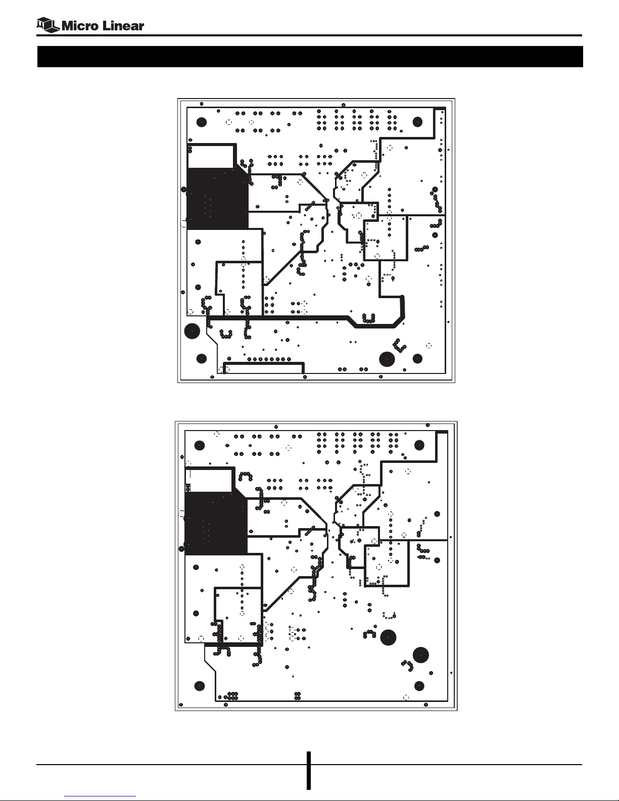
ML6651C Layer: VCC Plane
ML6651C Layer: Ground Plane
20
November 2001User’s Guide
Page 21
ML6651
APPENDIX B: FULL-SIZE BOARD WITH 1X9 MODULE: BOM, SCHEMATIC, & ARTWORKS
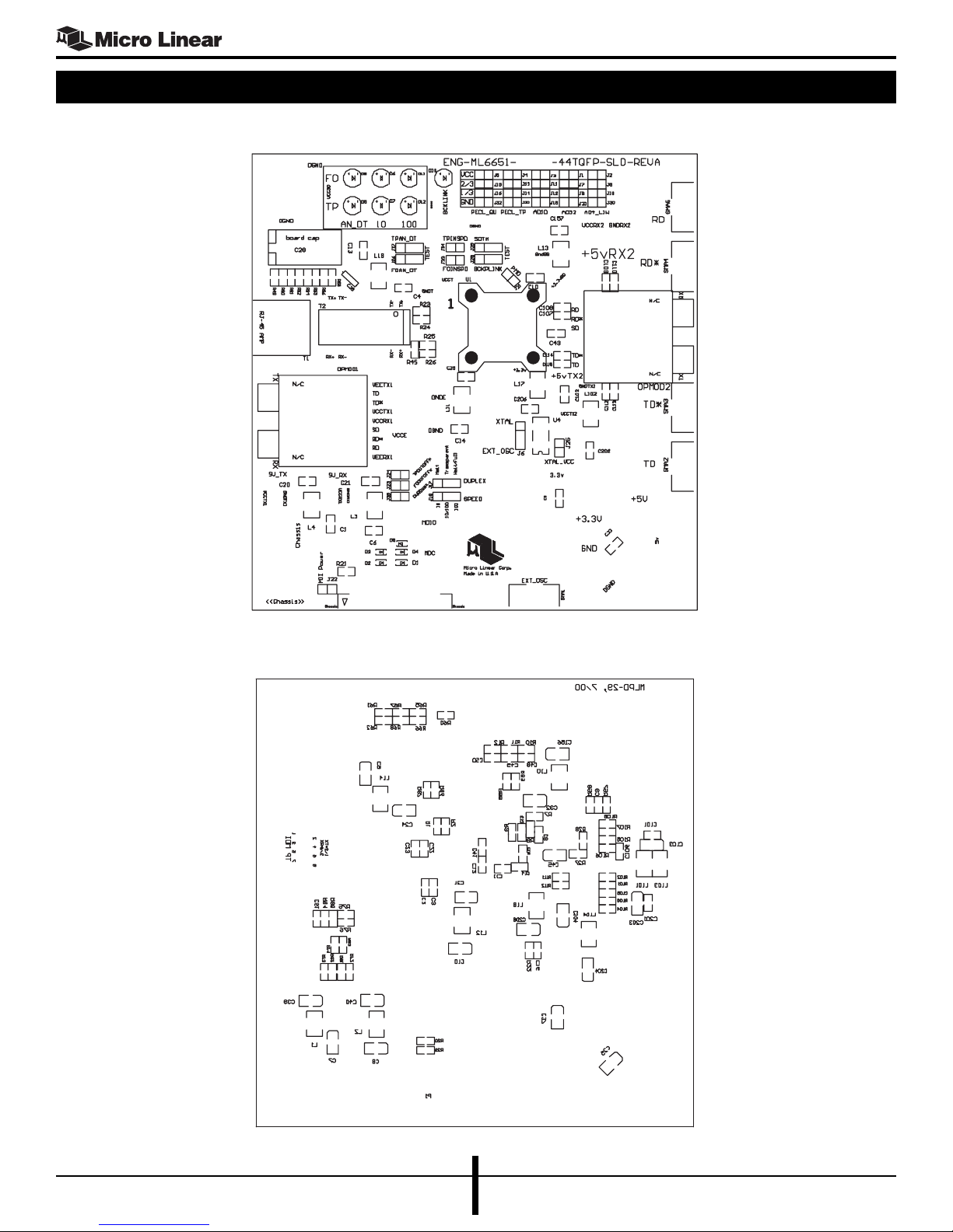
ML6651C Layer: Top Silk
ML6651C Layer: Bottom Silk
November 2001 User’s Guide
21
Page 22
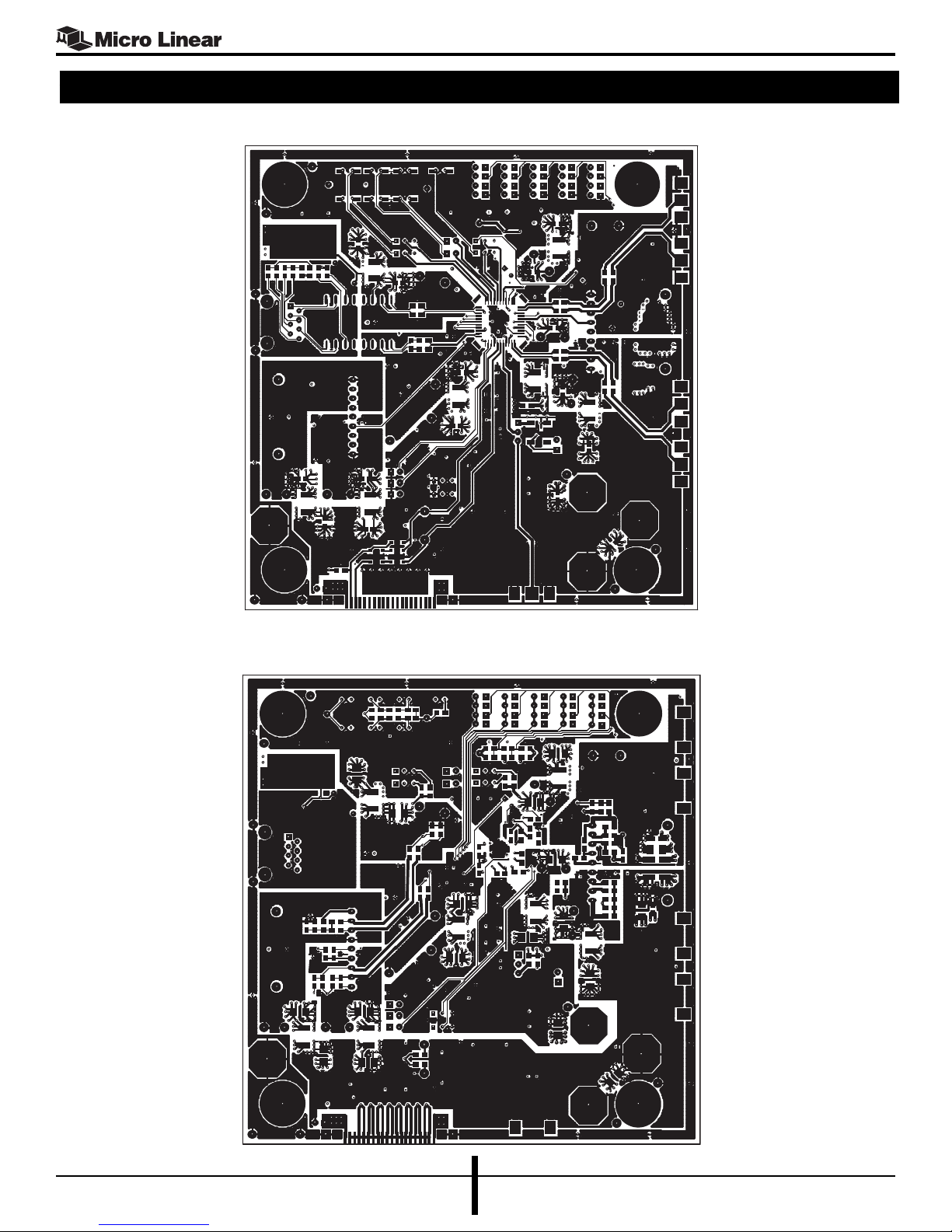
ML6651
APPENDIX B: FULL-SIZE BOARD WITH 1X9 MODULE: BOM, SCHEMATIC, & ARTWORKS
ML6651C Layer: Top
ML6651C Layer: Bottom
22
November 2001User’s Guide
Page 23
APPENDIX C: FULL SIZE BOARD REV. CMT WITH MT-RJ MODULE
ML6651
The following changes are made to the full-size board rev. A
(Appendix B) to construct rev. CMT board for MTRJ evalboard:
BOM changes:
· Remove L101,102
· R57 value is 2KΩ.
· R27,105,107 values are all 130 Ω.
· R28,106,108 values are all 82Ω.
· R103 value is 1KΩ.
· R104 value is 1.6KΩ.
Install wire jumpers from:
· C104 + TO C45+
· C103+ TO C32+
Reverse C103 placement since silk-screen is backward.
Note: This full size board rev CMT with the MT-RJ modules
shares the same PC board as the Appendix B. Use the
Appendix B board layout with the MT-RJ daughter board.
November 2001 User’s Guide
23
Page 24
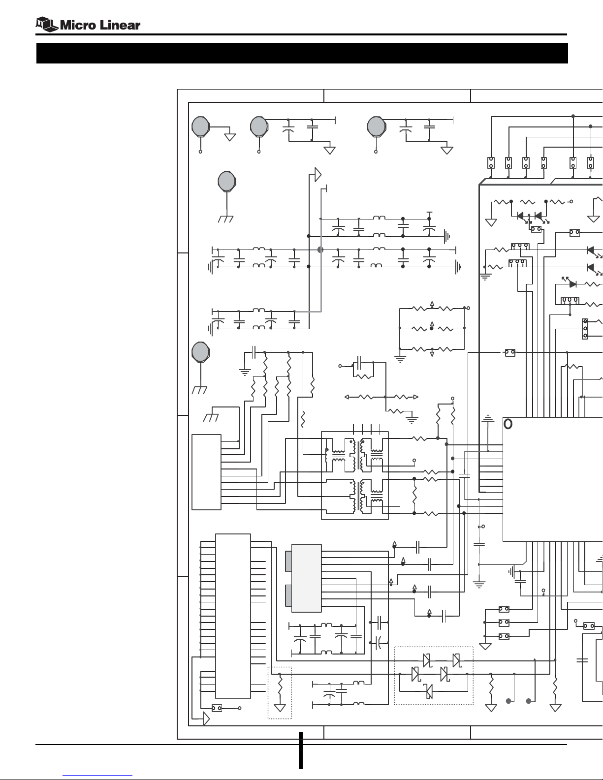
APPENDIX C: FULL SIZE BOARD REV. CMT WITH MT-RJ MODULE
123
321
D
C
B
A
TXTP+
1
TXTP-
2
RXTP+
3
NC
4
NC
5
RXTP-
6
NC
7
NC
8
SHLD
9
SHLD
10
T1
RJ45-SHIELDED
RXGND
1
OPINP
2
OPINN
3
SD
4
VCCRX
5
VCCTX
6
OPOUTN
7
OPOUTP
8
TXGND
9
RXTX
OPMOD1
7
8
6
3
2
1
1:1
TX+
RX+
14
15
16
9
10
11
T2
R151R2
51
VCCT
VCCT
R7 2K
J1 J7 J8
AD32
J3 J11 J12
AD10
R23
0
R240
R45
100
C2
0.1
C3
0.1
R25
0
R260
VCC
1
MDIO
2
MDC
3
RXD3
4
RXD2
5
RXD1
6
RXD0
7
RXDV
8
RXCK
9
RXER
10
TXER
11
TXCK
12
TXEN
13
TXD0
14
TXD1
15
TXD2
16
TXD3
17
COL
18
CRS
19
VCC
20
VCC
21
GND
22
GND
23
GND
24
GND
25
GND
26
GND
27
GND
28
GND
29
GND
30
GND
31
GND
32
GND
33
GND
34
GND
35
GND
36
GND
37
GND
38
GND
39
VCC
40
P1
MII-CONN
D1
D2
D3 D4
D5
R20
1.4K
R21
5K
R39
1.4K
R4950R5050R5150R52
50
R5350R54
50
C28
330pF, 3KV
R55
75
D6
D8
D9
D10
VCC3D
VCC3D
VCCE
C29
.1
+
C31
10uF
+
C32
10uF
C38
0.1
C11
0.1
C12
0.1
C16
0.1
L1
L2
L3
L4
VCC5D
C20
0.1
C39
10uF
C21
0.1
C40
10uF
J22
C22
0.1
C23
0.1
R56
75
R60
475
R61
150
C41
0.1
L10
L11
L12
L13
VCCBQ
+
C45
10uF
C43
0.1
L18
L17
VCCFC_L
DGND
D11
R67
511
R65
150
R6
15
R72
130
VCCRX1
R81
82
R73
130
R82
82
R74
130
R83
82
VRX1+
VRX1-
VSD1
VTX1+
VTX1-
VSD1
VRX1-
VRX1+
J25
1
J26
1
J27
1
J28
1J29
R87 1K
R86
1K
R88
1K
R8
1K
J19
J33
J34
TPOUTP
1
GNDT
2
TPOUTN
3
AD4LIW
4
AD32
5
AD10
6
PECLTP
7
PECLQU
8
VCCE
9
TPINP
10
TPINN
11
GNDE
12
TPOUTOFF#
13
FOOUTOFF#
14
GNDD
15
MDIO16MDC17REFCLK
18
VCCD19GNDL
20
IOUT21IOUT#
22
VCC
PWRDW
DUPL
VCC
SPEE
GND
SDF
CQO
VCC
FOIN
FOIN
GNDQ
34
GNDB
35
RTOP
36
REQSD
37
RTTP
38
SDTH
39
BCKPLINK
40
TPINSPD
41
FOINSPD
42
TPANDT
43
FOANDT
44
44 PIN TQFP
ML6651
+
C24
10uF
C4
0.1
L14
L19
VCCT
DGND IN
Chassis GND
J21
SD
JACK3
BANANA
JACK2
BANANA
GNDT
Chassis GND (earth)
DGND
DGND
GNDRX1
DGND
DGND
DGND
GNDT
DGND
DG
DGND
VCC5D
DGND
GNDFC_L
GNDT
GNDE
GNDBQ
VCC
4
N/C
1
TEST
TP1
TEST
TP2
R75
475
VCCTX1
R84
1.4K
R76
475
R85
4.02K
VTX1-VTX1+
GNDTX1
C51
0.1
VCCE
VCC3D
GNDT
GNDE
VCCMII
13 12 5 4
N/C
<-----N/C----->
C6
0.1
C1
0.1
C8
10uF
C7
10uF
DGND
VCC5D
DGND
+
C208
10uF
C206
0.1
+
C9
10uF
C13
0.1
+
C156
10uF
C157
0.1
+
C10
10uF
C14
0.1
J23
J24
J35
See Note 1
See Note 1
+3.3v DIGITAL IN
C37
10uF
C5
.01
JACK4
BANANA
DGND
VCC3D
+5v DIGITAL IN
C25
10uF
C33
.01
JACK1
BANANA
DGND
VCC5D
VCC3D
JACK3
BANANA
Chassis GND (earth)
DGND
ML6651
24
November 2001User’s Guide
Page 25
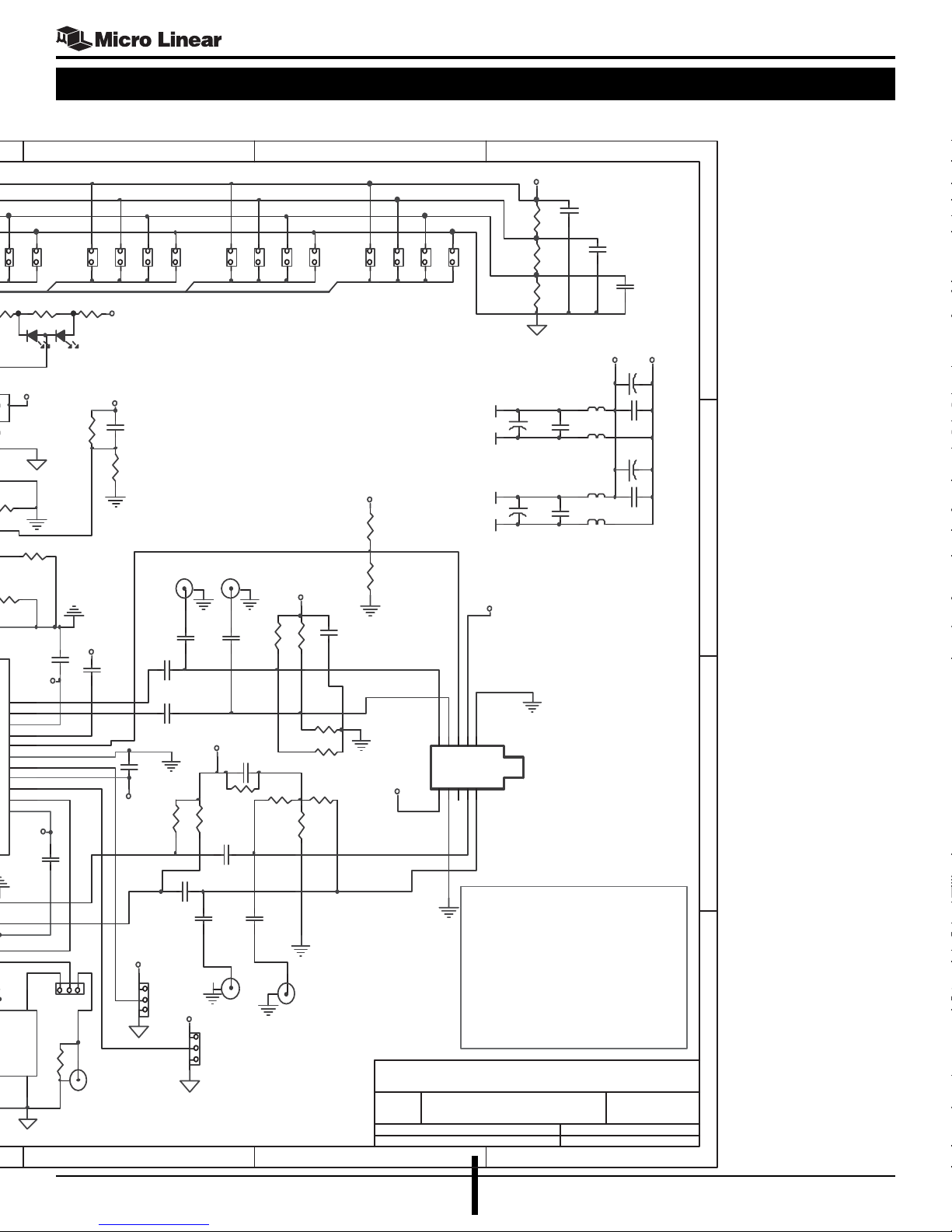
APPENDIX C: FULL SIZE BOARD REV. CMT WITH MT-RJ MODULE
VCC
N/C
654
VCC3D
C48
R10
0.1
20K
ML6651
AD4_LIW
R68
511
D7
DGND
GNDBQ
5K
C13
0.1
C14
0.1
J6
U4
25MHz
OUT
R22
49.9
GND
(edge-mount SMA)
DGND
J2 J9 J10
R62
150
VCCRX2
R58
1.4K
GNDBQ
VCCBQ
C8
0.1
1
ExtClkin
VCC3D
C9
0.1
R57
2.0K
GNDRX2
C108
.01
C107
GNDFC_L
C15
0.1
VCCFC_L
C114
VCC3D
1
J18
DGND
456
J20 J30 J31 J32
6
0
D12
VCC3D
9
R9
1.4K
VCCBQ
33
P
32
N
31
Q
30
S
29
O
28
FC
27
D
26
25
EX
24
N#
23
L
VCCFC_L
GNDFC_L
3
Oscillator
2
J4 J13 J14
PECL_TP
RD
BNC
GNDRX2 GNDRX2
C109
C110
0.1
0.1
Very Short Length!
(line to caps)
.01
VCCTX2
R103 1K
R11275R111
75
C115
0.1
0.1
Very Short Length!
(line to caps)
C113
0.1
GNDTX2
VCC3D
1
J17
DGND
RD*
C105
TD*
BNC
BNC
0.1
R101
475
C112
0.1
GNDTX2
VCCRX2
R107
130
TD
BNC
R105
130
R106 82
R108 82
R102
475
R104
1.6K
GNDTX2
J5 J15 J16
PECL_QU
VCCRX2
R27
130
R28
82
GNDRX2
C106
0.1
GNDRX2
3.3v
VCCTX2
Title
ML6651 EVAL BOARD SCHEMATIC (MT-RJ on right)
B
VccTX
GNDTX2
C102
0.1
C101
0.1
C49
0.1
VCC5D DGND
L102
0.1
L104
C203
L101
L103
RevisionSize
CMT
C50
0.1
C204
+
10uF
C202
+
10uF
C201
R11
20K
R12
20K
DGND
VCCTX2
GNDTX2
VCCRX2
GNDRX2
VccRX
SD
RD-
RD+
5
412
3
MT-RJ
678910
N/C
VeeTX
TD+
12 Planes on PCB, Digital: 5v & 3.3v. Analog: 9 pin
modules need 5v TX & RX (both sides), and the DUT
needs 5 analog planes; T, E, L, FC & BQ. RJ45 + half
magnetics on isolated & no inner planes. Each plane
has separate bead (vcc & gnd) and filter caps.
Digital Gnds share same gnd plane.
For 5v PMD; R58=1.3K, R57=3.7K
For 3.3v PMD; R58=1.3K, R57=2K
"L" & "FC" planes are combined into FC_L plane.
NOTE 1: D1-5 & R21 may not be needed.
3.3v
VCCRX2
GNDRX2
VeeRX
TD-
+
C104
10uF
+
C103
10uF
OPMOD2
D
0.1
C
B
A
November 2001 User’s Guide
25
Page 26
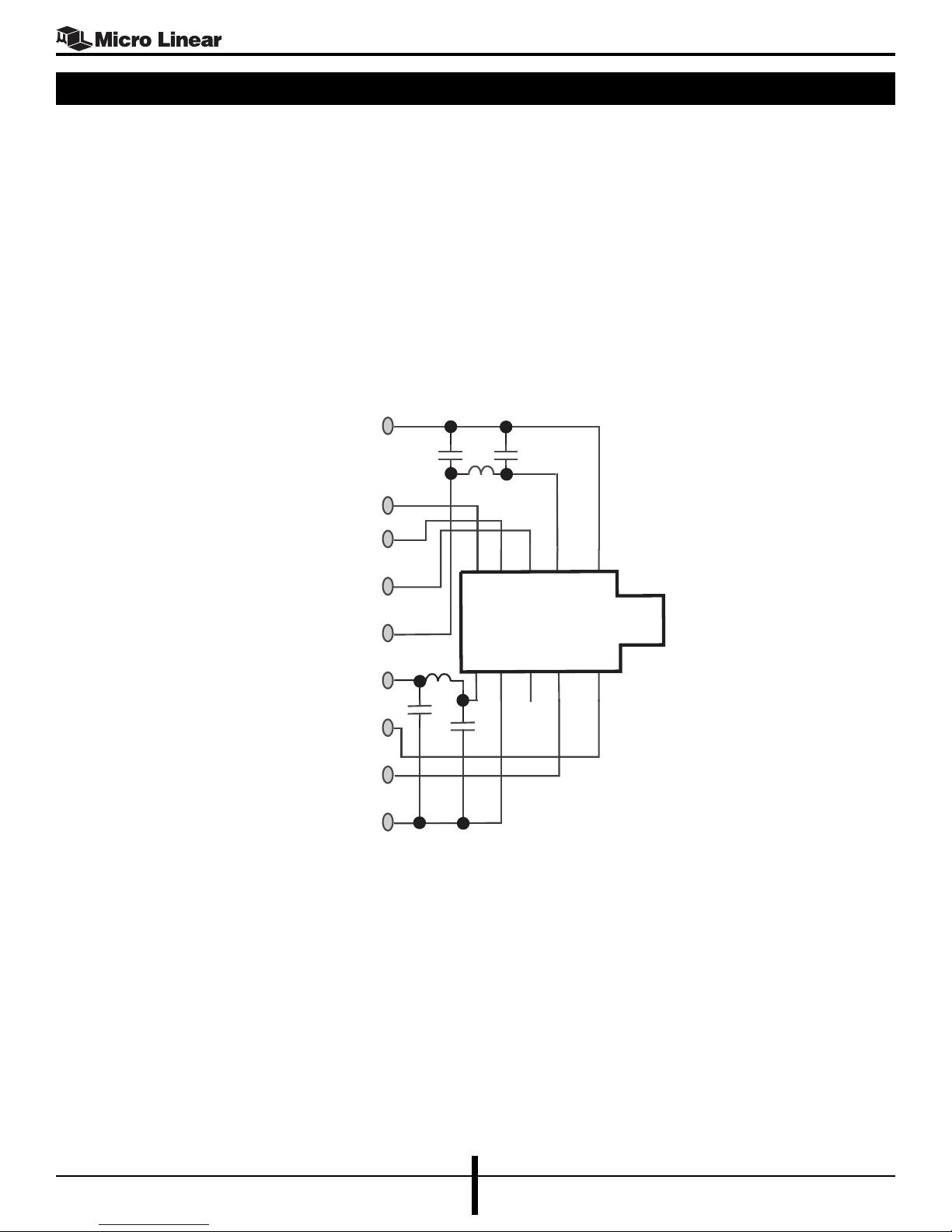
APPENDIX C: FULL SIZE BOARD REV. CMT WITH MT-RJ MODULE
ML6651
GNDRX
RD+
RD-
SD
VCCRX
VCCTX
TD-
TD+
GNDTX
C2
0.1
L2
C4
0.1
C3
C1
L1
0.1
0.1
RD-
RD+
HFBR-5
MT-RJ
(3.3V)
VeeTx
VccTx
SD
9
n/c
03
VccRx
TD+
VeeRx
TD-
26
November 2001User’s Guide
Page 27
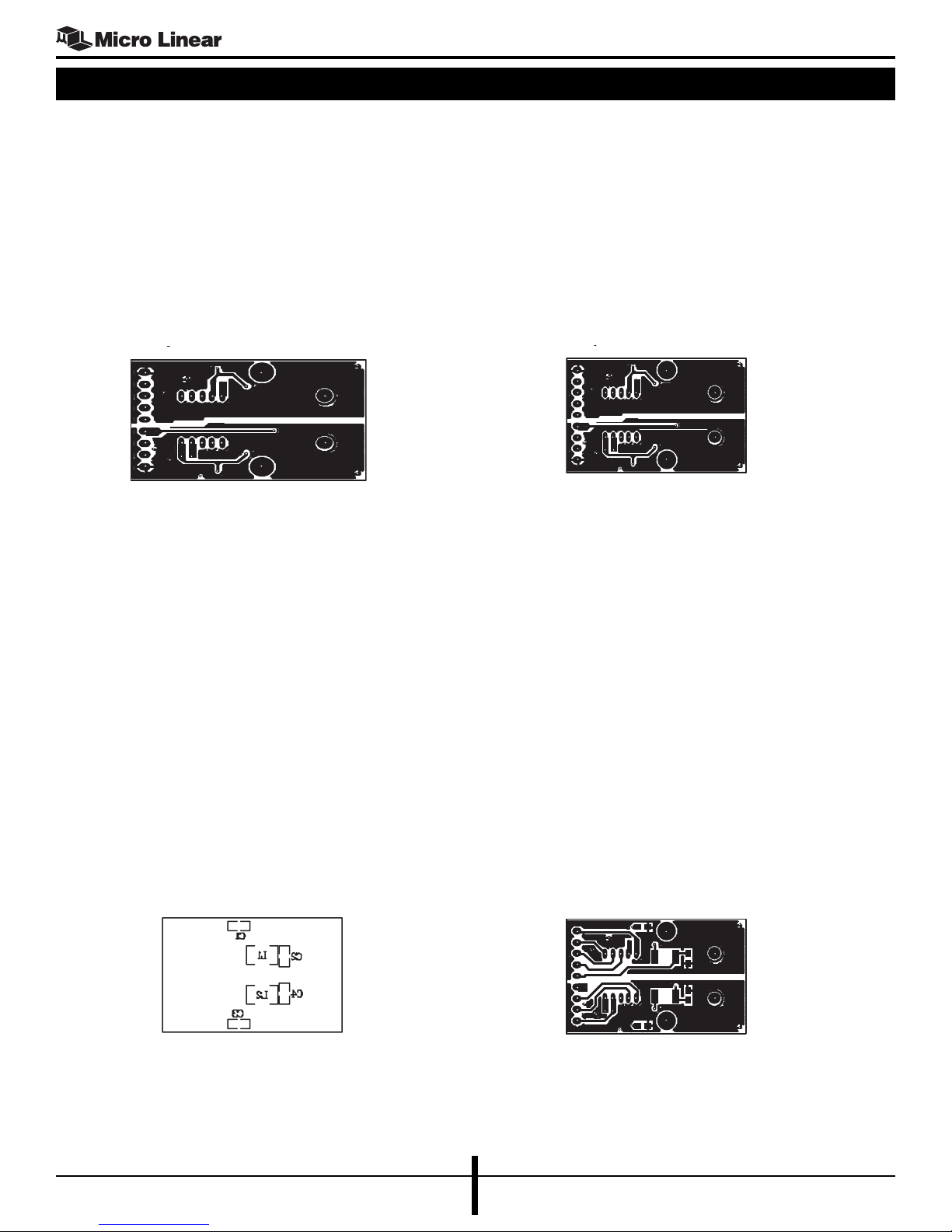
APPENDIX C: FULL SIZE BOARD REV. CMT WITH MT-RJ MODULE
k
ML6651
ML6651MTRJ Layer: Top
ML6651MTRJ Layer: Top
ML6651MTRJ Layer: Bottom Sil
ML6651MTRJ Layer: Bottom
November 2001 User’s Guide
UG6651-01
27
Page 28

ML6651
APPENDIX D: MINI-SIZE BOARD WITH SUGAR CUBES: SCHEMATIC, BOM & ARTWORKS
Part Type Designator Quantity Manufacturer Part Number
ΩΩ
0
Ω, 0805 R23,24,33 3 Digi-Key P0.0ACT-ND
ΩΩ
ΩΩ
10
Ω 1%, 0805 R10,25 2 any
ΩΩ
µµ
0.001
µF 20%, 0805 C052 1 Digi-Key PCC102BNCT-ND
µµ
µµ
0.01
µF 20%, 0805 C5,26,27 3 Digi-Key PCC103BNCT-ND
µµ
µµ
0.1
µF 20%, 0805 C4, 11,12,14-19,29,30, 24 Digi-Key PCC1840CT-ND
µµ
32,34-36, 41-43,48-50,150-152
µµ
0.47
µF 20%, 0805 C047 1 Digi-Key PCC1818CT-ND
µµ
ΩΩ
1.4K
Ω 1%, 0805 R8-58 2 Digi-Key P1.40KCCT-ND
ΩΩ
ΩΩ
100
Ω 1%, 0805 R45 1 Digi-Key P100ACT-ND
ΩΩ
µµ
10
µF 20% Tant 16V, B size C9-10,24,31, 13 Digi-Key PCS3106CT-ND
µµ
37,38, 44-46, 153-156
ΩΩ
150
Ω 1%, 0805 R61 4 Digi-Key P150ACT-ND
ΩΩ
Ω Ω
10K
Ω 1%, 0805 R88 1 Digi-Key
Ω Ω
Ω Ω
2K
Ω 1%, 0805 R07 1 Digi-Key P2.0KACT-ND
Ω Ω
Ω Ω
30
Ω 1%, 0805 R32 1 Digi-Key P30ACT-ND
Ω Ω
330pF 20%, 3KV cer disc C028 1 Digi-Key P4502A-ND
ΩΩ
4.02K
Ω 1%, 0805 R57 1 Digi-Key P4.02KCCT-ND
ΩΩ
ΩΩ
475
Ω 1%, 0805 R60 1 Digi-Key P475CCT-ND
ΩΩ
ΩΩ
5
Ω 1%, 0805 R47,48 2 Digi-Key P5.1ACT-ND
ΩΩ
ΩΩ
49.9
Ω 1%, 0805 R,1-2,49-54 8 Digi-Key P49.9CCT-ND
ΩΩ
ΩΩ
511
Ω 1%, 0805 R67,68 2 Digi-Key P511CCT-ND
ΩΩ
ΩΩ
5K
Ω 1%, 0805 R09 1 Digi-Key P4.99KCCT-ND
ΩΩ
ΩΩ
75
Ω 1%, 0805 R55,56 2 Digi-Key P75ACT-ND
ΩΩ
Ferrite Bead L5,6,10-19 12 Digi-Key P9812CT-ND
JUMPER 3 PIN J17-18,28 3 Digi-Key WM4001-ND
LED (green) D11,12 2 Digi-Key L62705CT-ND
LED (red) D8-10 3 Digi-Key L62701CT-ND
LED (yellow) D6,7 2 Digi-Key L62707CT-ND
Oscillator 25MHz U4 1 Digi-Key SE2837CT-ND (SG636)
RJ45-SHIELDED receptacle, T1 1 any
8-pin modular
28
November 2001User’s Guide
Page 29
ML6651
APPENDIX D: MINI-SIZE BOARD WITH SUGAR CUBES: SCHEMATIC, BOM & ARTWORKS
Part Type Designator Quantity Manufacturer Part Number
Test Pin 3.3V 1 Part of 36 pin Header XXXXXXXXXXXX
Test Pin 5V 1 Part of 36 pin Header XXXXXXXXXXXX
Test Pin Chassis 2 Part of 36 pin Header XXXXXXXXXXXX
Test Pin DGnd 6 Part of 36 pin Header XXXXXXXXXXXX
Test Pin GNDBQ Test Pin Part of 36 pin Header XXXXXXXXXXXX
Test Pin GNDE Test Pin Part of 36 pin Header XXXXXXXXXXXX
Test Pin GNDFC Test Pin Part of 36 pin Header XXXXXXXXXXXX
Test Pin GNDL 1 Part of 36 pin Header XXXXXXXXXXXX
Test Pin GNDRX1 1 Part of 36 pin Header XXXXXXXXXXXX
Test Pin GNDRX2 1 Part of 36 pin Header XXXXXXXXXXXX
Test Pin GNDT 1 Part of 36 pin Header XXXXXXXXXXXX
Test Pin GNDTX1 1 Part of 36 pin Header XXXXXXXXXXXX
Test Pin M10 1 Part of 36 pin Header XXXXXXXXXXXX
Test Pin MDC 1 Part of 36 pin Header XXXXXXXXXXXX
Test Pin VCC3D 1 Part of 36 pin Header XXXXXXXXXXXX
Test Pin VCCBQ 1 Part of 36 pin Header XXXXXXXXXXXX
Test Pin VCCE 1 Part of 36 pin Header XXXXXXXXXXXX
Test Pin VCCFC 1 Part of 36 pin Header XXXXXXXXXXXX
Test Pin VCCL 1 Part of 36 pin Header XXXXXXXXXXXX
Test Pin VCCRX1 1 Part of 36 pin Header XXXXXXXXXXXX
Test Pin VCCRX2 1 Part of 36 pin Header XXXXXXXXXXXX
Test Pin VCCT 1 Part of 36 pin Header XXXXXXXXXXXX
Test Pin VCCTX1 1 Part of 36 pin Header XXXXXXXXXXXX
Test Pins All Test Pins 36 pin header Digi-Key S1212-36-ND
10/100 magnetic T2 1 Pulse H1019
10/100BASE-SX media converter U1 1 Micro Linear ML6651
Fiber optic LED xmitter U2 1 Agilent HFBR-1414T (820nm)
Fiber optic PIN preamp rcvr U3 1 Agilent HFBR-2616T (820nm)
3.3VDC regulator N/A 1 Linear Tech LT1129CST-3.3
DC power jack N/A 1 Any 3-pin, 2.1mm
November 2001 User’s Guide
29
Page 30
ML6651
APPENDIX D: MINI-SIZE BOARD WITH SUGAR CUBES: SCHEMATIC, BOM & ARTWORKS
Part Type Designator Quantity Manufacturer Part Number
AC/DC 5V supply adapter N/A 1 Any PHIHONG PSC15A-
050S, 5V, 3A output
Ω Ω
511
Ω 1%, 0805 R67-68 2 Digi-Key P511CCT-ND
Ω Ω
Ω Ω
5K
Ω 1%, 0805 R09 O8O5 Digi-Key P4.99KCCT-ND
Ω Ω
30
November 2001User’s Guide
Page 31
ML6651
November 2001 User’s Guide
31
Page 32
ML6651
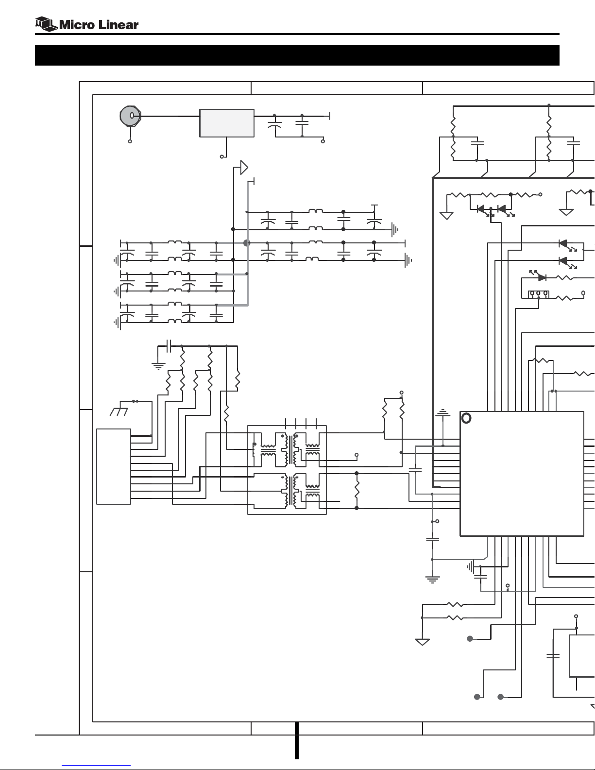
K
1
2
2
2
2
2
2
2
3
3
3
3
3
2
c
C
C
APPENDIX D: MINI-SIZE BOARD WITH SUGAR CUBES: SCHEMATIC, BOM & ARTWORKS
321
LT1129-3.3
VOLTREG
1
Vin
DGND
+
C153
10uF
+
C155
10uF
+
C9
10uF
C28
R5350R54
50
R4950R5050R5150R52
50
2
C157
0.1
C152
0.1
C13
0.1
GND
R55
75
11
10
Vout
R56
75
8
6
7
9
VCC3D
T2
RX+
3
+
+
TX+
+
C37
10uF
C157
C156
10uF
0.1
C14
C10
10uF
0.1
<-----N/C----->
13 12 5 4
1:1
1:1
L12
C5
.01
L13
L10
L11
DGND
VCC3D
C29
.1
1
3
2
16
14
N/C
15
C15
VCCT
R45
100
0.1
VCCBQ
+
+
R1
51
C46
10uF
C31
10uF
GNDBQ
VCCT
R2
51
C41
0.1
VCCE
GNDE
C12
0.1
GNDE
DGND
R10
10 ohm
R11
N/A
R65
150
DGND
GNDT
1
2
3
4
5
6
7
8
9
10
11
VCCE
DGND
R23 0
(0603 size)
R24 0
C50
0.1
AD32AD10 PECL_TP
D11
TPOUTP
GNDT
TPOUTN
AD4LIW
AD32
AD10
PECLTP
PECLQU
VCCE
TPINP
TPINN
C11
0.1
TP3
TEST
PWRDWN*
TP1
TEST
R67
511
D6
42
43
44
TPANDT
FOANDT
FOINSPD
GNDE12TPOUTOFF#
FOOUTOFF#
13
14
VCC3D
TP2
TEST
MDCMDIO
AD4_LIW
41
44 PIN TQFP
D
VCCFC
GNDFC
VCCL
GNDL
VCCT
GNDT
C
Chassis GND
T1
B
RJ45-SHIELDED
A
SHLD
SHLD
RXTP-
RXTP+
TXTP-
TXTP+
DGND
NC
NC
NC
NC
JACK
+
C44
10uF
+
C45
10uF
+
C24
10uF
330pF, 3KV
10
9
8
7
6
5
4
3
2
1
VCC5D
L16
C42
L15
0.1
L18
C43
L17
0.1
L19
C4
L14
0.1
GNDT
1 23
39
40
SDTH
TPINSPD
BCKPLINK
ML6651
GNDD15MDIO
MDC17REFCLK
16
R61
150
D10
1
J28
R7 2K
36
37
38
RTTP
REQSD
VCCD
18
19
20
C16
0.1
R12
N/A
R25
10 ohm
VCC3D
D8
D9
R60
475
R88
10K
34
35
RTOP
GNDB
GNDQ
FOINN
GNDFC
SPEED
VCCFC
DUPLEX
PWRDWN#
IOUT
GNDL
IOUT#
21
22
R66
150
DGND
VCC3D
FOINP
VCCQ
CQOS
SDFO
VCCL
VCC3D
C49
0.1
D
V
R9
R8
1.4
V
4
VCC
N/C
Os
1
32
November 2001User’s Guide
Page 33
C48
3
2
0.1
ML6651
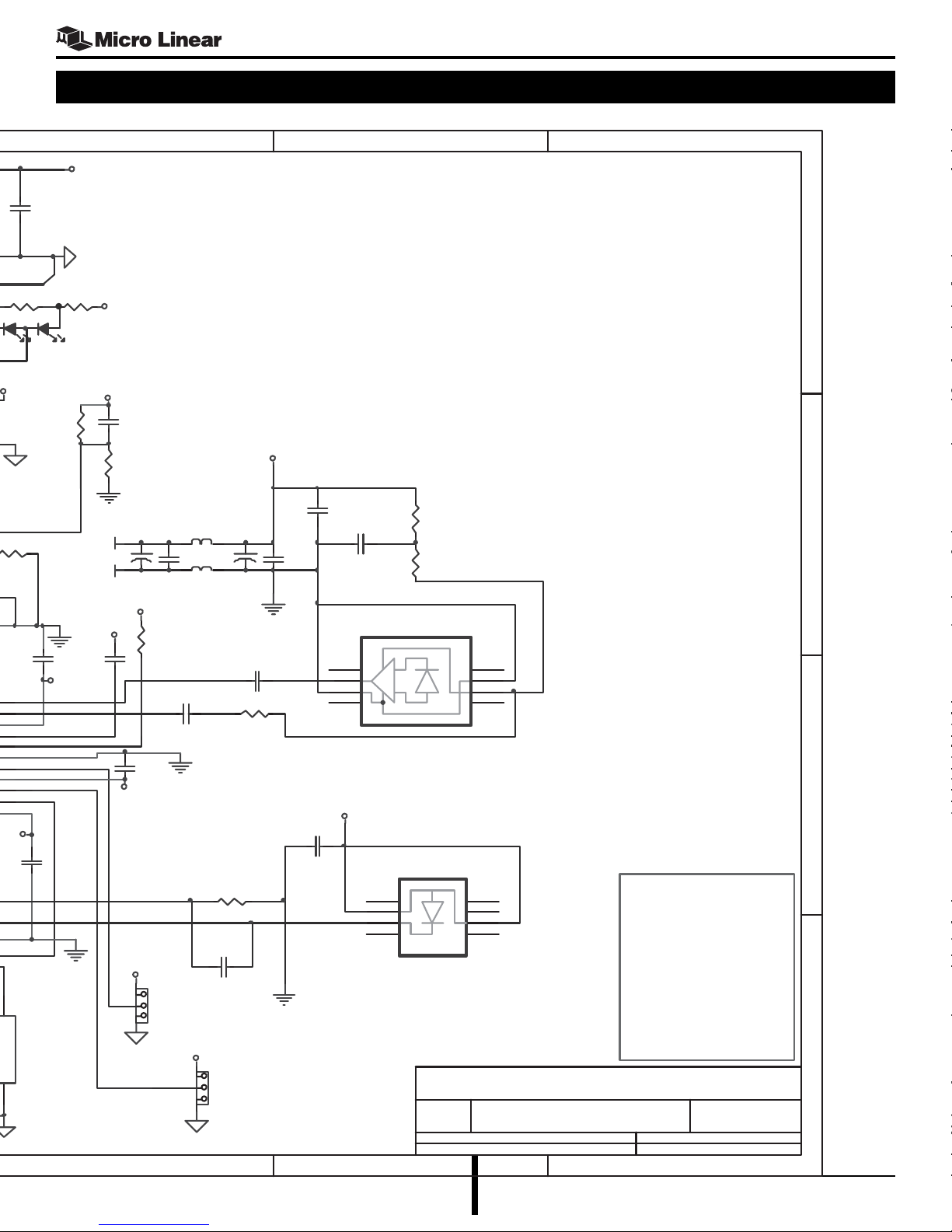
APPENDIX D: MINI-SIZE BOARD WITH SUGAR CUBES: SCHEMATIC, BOM & ARTWORKS
654
VCC3D
PECL_QU
R68
511
2
C3D
DGND
5K
3
2
1
0
9
8
7
6
5
4
3
CL
U4
25MHz
OUT
GND
illator
DGND
D7
C35
0.1
R58
1.4K
GNDBQ
C18
0.1
VCCBQ
GNDL
DGND
R62
150
VCCRX2
VCC5D
DGND
VCCBQ
C30
0.1
VCC3D
C36
0.1
C38
10uF
R46
C52
0.001uf
1
J17
DGND
C26
+
R32
1K
VCCRX2
GNDRX2
.01
30
C17
0.1
C19
0.1L5
(PLACE BYPASS CAPS CLOSE TO F/O MODULES)
GNDL
C47
0.47
Fiber Optic Receiver
U3
1
N/C
2
3
4
N/C N/C
VCCL
C34
0.1
U2
N/C
R48
5.0
R47
5.0
VCC
VEE
Fiber Optic Transmitter
Anode
1
2
3
4
Cathode
Title
ML6651 MINI EVAL BOARD SCHEMATIC
B
Date:
File:
8
N/C
7
6
5
8
N/C
7
N/C
6
5
N/CN/C
Number RevisionSize
R57
4.02K
GNDRX2
L6
+
C154
10uF
VCCFC
R33
VCCFC
VCC3D
DGND
C151
0.1
0
.01
C27
C32
0.1
456
J18
GNDFC
1
VCC3D
11 Planes on PCB, Digital: 5v & 3.3v.
Analog: 5v RX (sugar cube), 9 pin
mod
needs 5v TX & RX, and the DUT
needs
5 analog planes; T, E, L, FC & BQ.
RJ45 + half magnetics on isolated
& no inner planes.
TX sugar cube uses L (3.3v, analog)
for power.
Each plane has separate bead (vcc &
gnd) and filter caps. Digital Gnds
share same gnd plane.
E
D
C
B
A
November 2001 User’s Guide
33
Page 34
ML6651
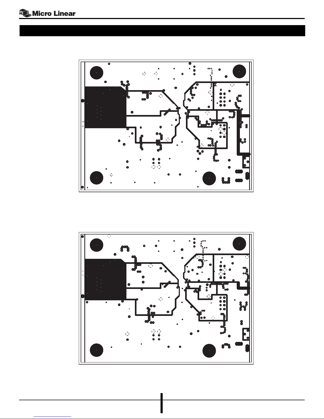
APPENDIX D: MINI-SIZE BOARD WITH SUGAR CUBES: SCHEMATIC, BOM & ARTWORKS
ML6651E Layer: VCC Plane
ML6651E Layer: Ground Plane
34
November 2001User’s Guide
Page 35
ML6651
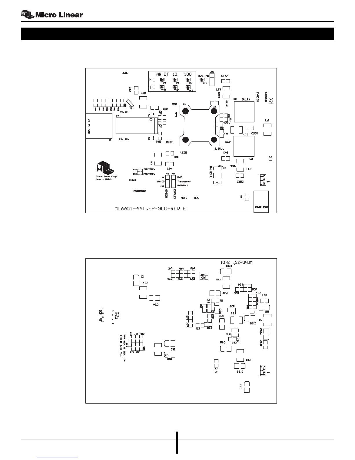
APPENDIX D: MINI-SIZE BOARD WITH SUGAR CUBES: SCHEMATIC, BOM & ARTWORKS
ML6651E Layer: Top Silk
ML6651E Layer: Bottom Silk
November 2001 User’s Guide
35
Page 36
ML6651
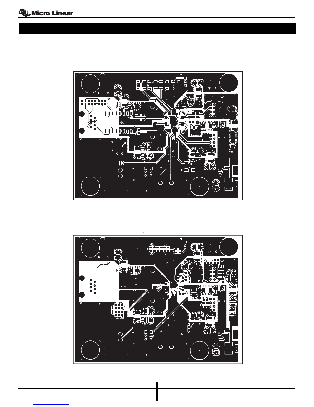
APPENDIX D: MINI-SIZE BOARD WITH SUGAR CUBES: SCHEMATIC, BOM & ARTWORKS
ML6651E Layer: Top
ML6651E Later: Bottom
36
November 2001User’s Guide
 Loading...