

Page 1
Operating Manual
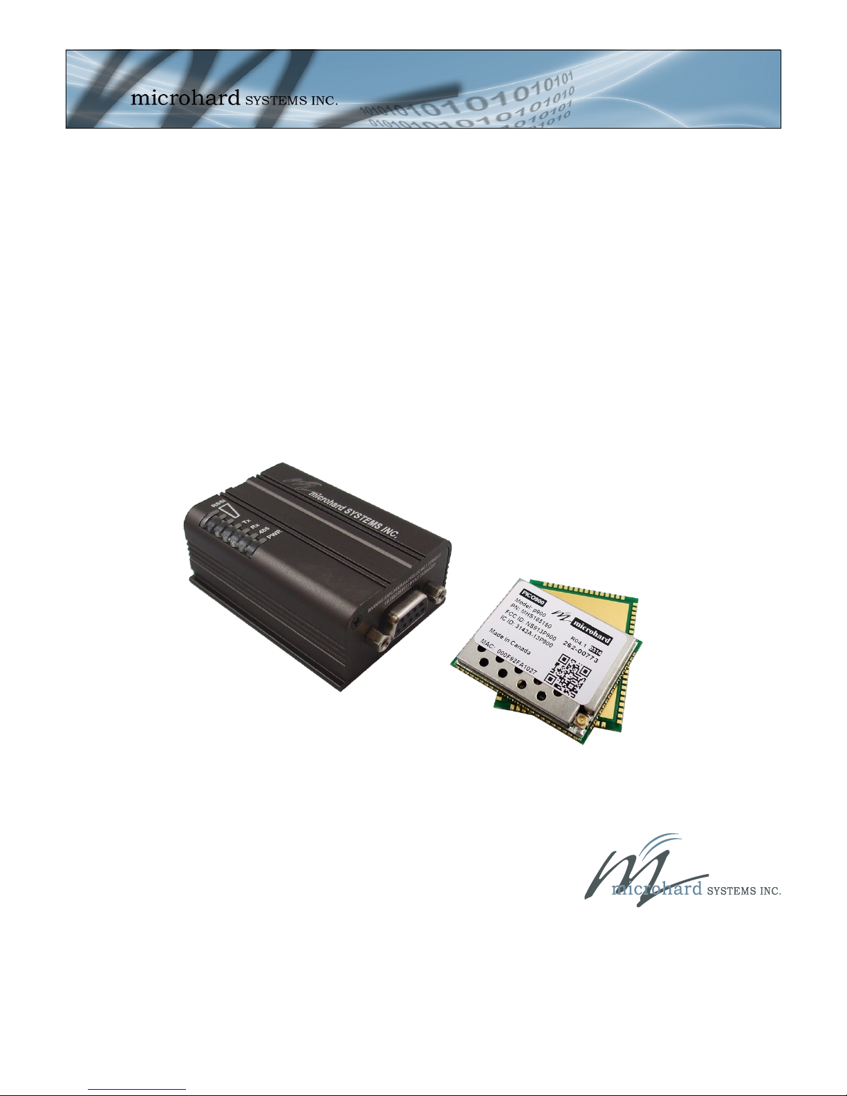
Pico Series - P900
900MHz Spread Spectrum Modem
Document: Pico Series P900 Operating Manual.v1.8.7
Date: June 2016
Firmware: v1.19
150 Country Hills Landing NW
Calgary, Alberta
Canada T3K 5P3
Phone: (403) 248-0028
Fax: (403) 248-2762
www.microhardcorp.com
Page 2

Important User Information
Warranty
Microhard Systems Inc. warrants that each product will be free of defects in material and workmanship for a period of one (1) year for its
products. The warranty commences on the date the product is shipped by Microhard Systems Inc. Microhard Systems Inc.’s sole l iability and
responsibility under this warranty is to repair or replace any product which is returned to it by the Buyer and which Microha rd Systems Inc.
determines does not conform to the warranty. Product returned to Microhard Systems Inc. for warranty service will be shipped to Microhard
Systems Inc. at Buyer’s expense and will be returned to Buyer at Microhard Systems Inc.’s expense. In no event shall Microhar d Systems
Inc. be responsible under this warranty for any defect which is caused by negligence, misuse or mistreatment of a product or for any unit
which has been altered or modified in any way. The warranty of replacement shall terminate with the warranty of the product.
Warranty Disclaims
Microhard Systems Inc. makes no warranties of any nature of kind, expressed or implied, with respect to the hardware, softwar e, and/or
products and hereby disclaims any and all such warranties, including but not limited to warranty of non -infringement, implied warranties of
merchantability for a particular purpose, any interruption or loss of the hardware, software, and/or product, any delay in pr oviding the hardware, software, and/or product or correcting any defect in the hardware, software, and/or product, or any other warranty. The Purchaser
represents and warrants that Microhard Systems Inc. has not made any such warranties to the Purchaser or its agents MICROHARD SY STEMS INC. EXPRESS WARRANTY TO BUYER CONSTITUTES MICROHARD SYSTEMS INC. SOLE LIABILITY AND THE
BUYER’S SOLE REMEDIES. EXCEPT AS THUS PROVIDED, MICROHARD SYSTEMS INC. DISCLAIMS ALL WARRANTIES,
EXPRESS OR IMPLIED, INCLUDING ANY WARRANTY OF MERCHANTABILITY OR FITNESS FOR A PARTICULAR PROMISE.
MICROHARD SYSTEMS INC. PRODUCTS ARE NOT DESIGNED OR INTENDED TO BE USED IN ANY LIFE SUPPORT
RELATED DEVICE OR SYSTEM RELATED FUNCTIONS NOR AS PART OF ANY OTHER CRITICAL SYSTEM AND ARE
GRANTED NO FUNCTIONAL WARRANTY.
Indemnification
The Purchaser shall indemnify Microhard Systems Inc. and its respective directors, officers, employees, successors and assign s including any
subsidiaries, related corporations, or affiliates, shall be released and discharged from any and all manner of action, causes of action, liability,
losses, damages, suits, dues, sums of money, expenses (including legal fees), general damages, special damages, including wit hout limitation, claims for personal injuries, death or property damage related to the products sold hereunder, costs and demands of eve ry and any kind
and nature whatsoever at law.
IN NO EVENT WILL MICROHARD SYSTEMS INC. BE LIABLE FOR ANY INDIRECT, SPECIAL, CONSEQUENTIAL, INCIDENTAL, BUSINESS INTERRUPTION, CATASTROPHIC, PUNITIVE OR OTHER DAMAGES WHICH MAY BE CLAIMED TO ARISE
IN CONNECTION WITH THE HARDWARE, REGARDLESS OF THE LEGAL THEORY BEHIND SUCH CLAIMS, WHETHER IN
TORT, CONTRACT OR UNDER ANY APPLICABLE STATUTORY OR REGULATORY LAWS, RULES, REGULATIONS, EXECUTIVE OR ADMINISTRATIVE ORDERS OR DECLARATIONS OR OTHERWISE, EVEN IF MICROH ARD SYSTEMS INC. HAS
BEEN ADVISED OR OTHERWISE HAS KNOWLEDGE OF THE POSSIBILITY OF SUCH DAMAGES AND TAKES NO ACTION TO
PREVENT OR MINIMIZE SUCH DAMAGES. IN THE EVENT THAT REGARDLESS OF THE WARRANTY DISCLAIMERS AND
HOLD HARMLESS PROVISIONS INCLUDED ABOVE MICROHARD SYSTEMS INC. IS SOMEHOW HELD LIABLE OR RESPONSIBLE FOR ANY DAMAGE OR INJURY, MICROHARD SYSTEMS INC.'S LIABILITY FOR ANYDAMAGES SHALL NOT EXCEED
THE PROFIT REALIZED BY MICROHARD SYSTEMS INC. ON THE SALE OR PROVISION OF THE HARDWARE TO THE CUSTOMER.
Proprietary Rights
The Buyer hereby acknowledges that Microhard Systems Inc. has a proprietary interest and intellectual property rights in the Hardware,
Software and/or Products. The Purchaser shall not (i) remove any copyright, trade secret, trademark or other evidence of Micr ohard Systems
Inc.’s ownership or proprietary interest or confidentiality other proprietary notices contained on, or in, the Hardware, Soft ware or Products,
(ii) reproduce or modify any Hardware, Software or Products or make any copies thereof, (iii) reverse assemble, reverse engin eer or decompile any Software or copy thereof in whole or in part, (iv) sell, transfer or otherwise make available to others the Hardware , Software, or
Products or documentation thereof or any copy thereof, except in accordance with this Agreement.
© Microhard Systems Inc. Confidential 2
Page 3

Important User Information (continued)
About This Manual
It is assumed that users of the products described herein have either system integration or design experience, as well as an understanding of the fundamentals of radio communications.
Throughout this manual you will encounter not only illustrations (that further elaborate on the accompanying text), but also several symbols which you should be attentive to:
Caution or Warning
Usually advises against some action which could result in undesired or
detrimental consequences.
Point to Remember
Highlights a key feature, point, or step which is noteworthy. Keeping
these in mind will simplify or enhance device usage.
Tip
An idea or suggestion to improve efficiency or enhance usefulness.
© Microhard Systems Inc. Confidential 3
Page 4
Important User Information (continued)
Regulatory Requirements
To satisfy FCC RF exposure requirements for mobile transmitting devices, a separation distance
of 23cm or more should be maintained between the antenna of this device and persons during
device operation. To ensure compliance, operation at closer than this distance is not
recommended. The antenna being used for this transmitter must not be co-located in conjunction
WARNING
with any other antenna or transmitter.
This device can only be used with antennas designed for use with 900 MHz products. Please
contact Microhard Systems Inc. if you need more information or would like to order an antenna.
WARNING
WARNING
MAXIMUM EIRP
FCC Regulations allow up to 36dBm Effective Isotropic Radiated Power (EIRP). Therefore, the
sum of the transmitted power (in dBm), the cabling loss and the antenna gain cannot exceed
36dBm.
EQUIPMENT LABELING
This device has been modularly approved. The manufacturer, product name, and FCC and
Industry Canada identifiers of this product must appear on the outside label of the end-user
equipment.
SAMPLE LABEL REQUIREMENT:
For P900
FCCID: NS913P900
IC: 3143A-13P900
This device complies with Part 15 of the FCC Rules.
Operation is subject to the following two conditions:
(1) this device may not cause harmful interference,
and (2) this device must accept any interference
received including interference that may cause
undesired operation.
Please Note: These are only sample labels; different products contain different identifiers. The
actual identifiers should be seen on your devices if applicable.
© Microhard Systems Inc. Confidential 4
Page 5

Revision History
Revision Description Initials Date
1.0 Draft PEH Mar 2013
1.1 Firmware v1.0 PEH Sept 2013
1.2 Official Release. Firmware v1.0. Added PTP, PMP Modes PEH Sept 2013
1.21 Added Pad Landing and Solder Mask/Paste diagrams, expanded Mesh
description, modified pins descriptions, added AT command firmware
upgrade, misc formatting corrections.
1.22 Misc Corrections PEH Feb 2014
1.3 Added RS485 Support (S142). Firmware required v1.06. PEH July 2014
1.4 Update for firmware v1.09 SG/PEH Dec 2014
1.5 Update for firmware v1.10—Added link rate 57.6 kbps, minor bugs
fixed. Added register S225 - Compression (must be set to zero for compatibility with older versions).
1.6 Update for firmware v1.11 - Added link rate 115.2 kbps. Added AT&S3
to enable RS485 driver.
1.7 Update for firmware v1.14 - Removed AT&S3, Added AT&K1 to use
CTS to control the Transmitter of RS485 driver chip.
1.8 Added P900-ENC drawings, connectors and LED descriptions PEH Sept 2015
1.81 Added P900-ENC Optional mounting Bracket. Misc updates. PEH Oct 2015
1.8.2 Modified description of S232. PEH Jan 2016
1.8.3 Updated Enclosed DB9 RS232/485 Pins. PEH Feb 2016
1.8.4 Added S159, S177 for AES Encryption PEH Feb 2016
1.8.5 Pin corrections PEH Feb 2016
1.8.6 Added MST reflow and baking instructions, misc corrections. PEH June 2016
1.8.7 Added Pico-MHX Adapter Board PEH June 2016
PEH Sept 2013
SG/PEH Jan 2015
PEH Jan 2015
PEH Aug 2015
© Microhard Systems Inc. Confidential 5
Page 6

Table of Contents
1.0 Overview 10
1.1 Performance Features ........................................................................................................ 10
1.2 Specifications ..................................................................................................................... 11
2.0 Hardware Description 12
2.1 OEM Mechanical Drawing .................................................................................................. 13
2.1.1 Recommended Solder Mask (Pad Landing) .............................................................................14
2.1.2 Recommended Solder Paste Pattern .......................................................................................15
2.1.3 OEM Connectors ....................................................................................................................15
2.1.4 SMT Temperature Profile ........................................................................................................16
2.1.5 Baking Instructions (MSL) .......................................................................................................16
2.2 OEM Pin Descriptions ........................................................................................................ 17
2.3 OEM Minimum Connection Requirements ........................................................................ 20
2.4 Electrical Characteristics ................................................................................................... 21
2.4.1 Test Conditions.....................................................................................................................21
2.4.1.1 Minimum and Maximum Values ...............................................................................21
2.4.1.2 Typical Values .........................................................................................................21
2.4.1.3 Loading Capacitor ...................................................................................................21
2.4.1.4 Pin Input Voltage .....................................................................................................21
2.4.2 Absolute Maximum Ratings..................................................................................................22
2.4.3 Operating Conditions ...........................................................................................................22
2.4.3.1 Operating Conditions at Power-up / Power-down ......................................................22
2.4.3.2 Voltage Characteristics ............................................................................................22
2.4.3.3 Current Characteristics ............................................................................................23
2.4.3.4 IO Port Characteristics .............................................................................................24
2.4.3.5 12-bit ADC Characteristics .......................................................................................25
2.5 P900 to n920 Pin-outs......................................................................................................... 27
2.6 P900 Enclosed ..................................................................................................................................28
2.6.1 P900 Enclosed Mechanical Drawings ......................................................................................29
2.6.2 P900 Enclosed Mounting Bracket (Optional) ............................................................................30
2.6.3 P900 Enclosed Connectors & Indicators ..................................................................................31
3.0 Mesh Configuration 33
3.1 Configuration/Unit Modes .................................................................................................. 33
3.1.1 Command Mode .....................................................................................................................33
3.1.2 Data mode ..............................................................................................................................34
3.2 Mesh Network ..................................................................................................................... 35
3.2.1 Operating Modes / Unit Types .................................................................................................35
3.2.2 Configuration Using Factory Defaults.......................................................................................39
AT&F1 - Primary Coordinator ..................................................................................................40
AT&F2 - Mesh Remote ...........................................................................................................41
AT&F3 - Secondary Coordinator..............................................................................................42
Standby Coordinator ...............................................................................................................43
3.2.3 Unit Addressing ......................................................................................................................44
3.2.4 Collision Mitigation ..................................................................................................................45
3.2.4.1 Channel Access Mode .............................................................................................45
3.2.4.2 Carrier Sense ..........................................................................................................46
3.2.4.3 TX Profile & Ranking ...............................................................................................48
3.2.5 Retransmissions .....................................................................................................................49
3.2.6 Network Synchronization.........................................................................................................49
3.2.7 Routing...................................................................................................................................50
3.2.8 Hop Pattern ............................................................................................................................55
© Microhard Systems Inc. Confidential 6
Page 7

Table of Contents (continued)
4.0 Point to Point Configuration 57
4.1 Configuration/Unit Modes .................................................................................................. 57
4.1.1 Command Mode .....................................................................................................................57
4.1.2 Data mode ..............................................................................................................................58
4.2 Point to Point Network ....................................................................................................... 59
4.2.1 Operating Modes / Unit Types .................................................................................................59
4.2.2 Configuration Using Factory Defaults.......................................................................................61
AT&F10 - PP Master ...............................................................................................................62
AT&F11 - PP Slave/Remote ....................................................................................................63
AT&F12 - PP Repeater ...........................................................................................................64
4.2.5 Retransmissions .....................................................................................................................65
4.2.6 Network Synchronization.........................................................................................................65
4.2.7 Hop Pattern ............................................................................................................................66
5.0 Point to Multipoint Configuration 68
5.1 Configuration/Unit Modes .................................................................................................. 68
5.1.1 Command Mode .....................................................................................................................68
5.1.2 Data mode ..............................................................................................................................69
5.2 Point to Multipoint Network ............................................................................................... 70
5.2.1 Operating Modes / Unit Types .................................................................................................70
5.2.2 Configuration Using Factory Defaults.......................................................................................73
AT&F7 - PMP Master ..............................................................................................................74
AT&F8 - PMP Slave/Remote ...................................................................................................75
AT&F9 - PMP Repeater ..........................................................................................................76
5.2.3 Unit Addressing ......................................................................................................................77
5.2.4 Retransmissions .....................................................................................................................77
5.2.5 Network Synchronization.........................................................................................................77
5.2.6 Hop Pattern ............................................................................................................................78
6.0 Register/Command Reference 80
6.1 AT Commands................................................................................................................... 80
A Answer .................................................................................................................................80
g, G Spectrum Analyzer ................................................................................................................80
In Identification .........................................................................................................................80
login Enable login password ..........................................................................................................81
M Mesh Diagnostics Menu ........................................................................................................81
N Advanced Spectrum Analyzer ................................................................................................82
&Fn Load Factory Default Configuration ........................................................................................82
&V View Configuration ................................................................................................................82
&W Write Configuration to Memory ..............................................................................................82
6.2 Settings (S) Registers ....................................................................................................... 83
S0 Power-up Mode.....................................................................................................................83
S2 Escape Character .................................................................................................................83
S80 Transmit Profiles ...................................................................................................................83
S81 CS Threshold ........................................................................................................................83
S83 Records TTL .........................................................................................................................84
S85 Distance to Master (PP/PMP) ................................................................................................84
S86 Distance from Master (PP/PMP) ............................................................................................84
S87 Enable S105 as MAC (Mesh) ................................................................................................84
S101 Operating Mode (Mesh) .........................................................................................................85
S101 Operating Mode (PP/PMP) ....................................................................................................85
S102 Serial Baud Rate ...................................................................................................................85
S103 Wireless Link Rate ................................................................................................................85
S104 Network ID/Address ..............................................................................................................86
© Microhard Systems Inc. Confidential 7
Page 8

Table of Contents (continued)
6.2 Settings (S) Registers (continued)
S105 Unit Address .........................................................................................................................86
S106 Hop Pattern ..........................................................................................................................86
S108 Output Power ........................................................................................................................86
S109 Hop Interval ..........................................................................................................................87
S110 Data Format ..........................................................................................................................87
S111 Packet Min Size ....................................................................................................................88
S112 Packet Max Size ...................................................................................................................88
S113 Packet Retransmissions ........................................................................................................88
S115 Repeat Interval......................................................................................................................88
S116 Character Timeout ................................................................................................................88
S118 Roaming (PP/PMP) ...............................................................................................................89
S123 Average RSSI (Mesh) ...........................................................................................................89
S123 RSSI from Master (dBm) (PP/PMP) .......................................................................................89
S124 RSSI from Slave (dBm) (PP/PMP) .........................................................................................89
S126 Attempt Before Re-Route (Mesh) ...........................................................................................89
S130 No Sync Data Intake .............................................................................................................89
S133 Network Type ........................................................................................................................90
S140 Destination Address ..............................................................................................................90
S141 Repeaters Y/N (PP/PMP) ......................................................................................................90
S142 Serial Channel Mode (RS232/485).........................................................................................90
S143 Sleep Mode ..........................................................................................................................90
S144 Sleep Time ...........................................................................................................................91
S145 Wake Time ...........................................................................................................................91
S146 Tx Done Timeout, 1/4 ............................................................................................................91
S151 Quick Sync Packets (Mesh) ...................................................................................................91
S153 Address Tag .........................................................................................................................91
S158 Forward Error Correction (FEC) Mode ...................................................................................92
S159 Encryption Mode (AES) .........................................................................................................92
S163 CRC Check on Diag Port .......................................................................................................93
S177 Binary Encryption Key ...........................................................................................................93
S180 Hop Zone ..............................................................................................................................93
S181 Secondary Hop Zone ............................................................................................................93
S183 DCD Pulse Period (PP/PMP) .................................................................................................93
S184 Data Time to Live (Mesh) ......................................................................................................94
S206 Secondary Hop Pattern .........................................................................................................94
S214 Number of Aloha Slots (Mesh) ...............................................................................................94
S215 Number of Mesh Slots (Mesh) ...............................................................................................94
S216 Mesh Duty Cycle (Mesh) .......................................................................................................94
S217 Protocol Type ........................................................................................................................95
S218 Input Framing ........................................................................................................................95
S219 Routing Request TTL (Mesh) .................................................................................................95
S220 Mesh Coordinator Rank (Mesh) .............................................................................................95
S221 Mesh TDMA Slot to Tx (Mesh) ...............................................................................................95
S222 Roaming Mode (Mesh) ..........................................................................................................95
S223 Routing (Mesh) .....................................................................................................................96
S224 Standby Trip Level (Mesh) .....................................................................................................96
S225 Compression Mode ...............................................................................................................96
S232 Max Buffer in Storage ............................................................................................................96
S234 Master Ch. Request Timeout (PMP) ......................................................................................97
S235 PP Routing TTL (PP) .............................................................................................................97
S236 Max Buffer Out Storage .........................................................................................................97
S244 Channel Access Mode...........................................................................................................97
S245 Cost of Hop in Mesh ..............................................................................................................97
S247 Country Code (Read Only) ....................................................................................................97
S248 Sync Timeout ........................................................................................................................98
© Microhard Systems Inc. Confidential 8
Page 9

Table of Contents (continued)
S249 Packets per Hop Tx Limit (PP/PMP) ......................................................................................98
S250 Master Bandwidth % (PMP) ...................................................................................................98
S251 Master Hop Allocation Timeout (PMP) ...................................................................................98
S252 Slave Ch. Allocation Timeout (PMP) ......................................................................................98
6.3 Serial Interface Commands .............................................................................................. 99
&Cn Data Carrier Detect (DCD) .....................................................................................................99
&Dn Data Terminal Ready (DTR) ..................................................................................................99
&K Handshaking .........................................................................................................................99
&Sn Data Set Ready (DSR) ..........................................................................................................99
7.0 Installation 100
7.1 Path Calculation .............................................................................................................. 102
7.2 Installation of Antenna System Components ................................................................ 103
7.2.1 Antennas ............................................................................................................................ 103
7.2.2 Coaxial Cable ..................................................................................................................... 104
7.2.3 Surge Arrestors ................................................................................................................... 104
7.2.4 External Filter ...................................................................................................................... 104
Appendices
Appendix A: AT Command Quick Reference ..................................................................................... 105
Appendix B: Settings (S) Register Quick Reference .......................................................................... 106
Appendix C: AT Utility Firmware Upgrade Procedure........................................................................ 107
Appendix D: AT Command Firmware Upgrade .................................................................................. 108
Appendix E: Development Board Serial Interface .............................................................................. 109
Appendix F: Pico Reference Schematic............................................................................................. 110
Appendix G: Pico-MHX Adapter Board ............................................................................................... 111
Appendix H: Approved Antennas ....................................................................................................... 113
© Microhard Systems Inc. Confidential 9
Page 10

1.0 Overview
The Pico Series P900 is capable of delivering high-performance wireless serial communications in robust and secure Mesh, Point to Point or Point to Multipoint topologies.
The Pico Series is available as a low cost OEM module, for the ultimate in design integration.
When properly configured and installed, long range communications at very high speeds can
be achieved.
Pico Series modules operate within the 902-928 MHz ISM frequency band, using frequency
hopping spread spectrum (FHSS) technology, providing reliable wireless asynchronous data
transfer between most equipment types which employ a serial interface.
The small size and superior performance of the Pico Series makes it ideal for many applications. Some typical uses for this modem:
SCADA
remote telemetry
traffic control
industrial controls
remote monitoring
fleet management
GPS
metering
1.1 Performance Features
Key performance features of the Pico Series include:
transmission within a public, license-exempt band of the radio spectrum1 - this
means that the modems may be used without access fees or recurring charges
(such as those incurred by cellular airtime)
transparent, low latency link rates up to 276 kbps
communicates with virtually all serial based devices
supports a robust true Mesh operation with auto-routing
wide temperature specification
maximum allowable transmit power (1 Watt)
32 bits of CRC, selectable retransmission and forward error correction
separate diagnostics port - transparent remote diagnostics and online network
control
ease of installation and configuration - the P900 utilizes a subset of standard AT-
style commands, similar to those used by traditional telephone line modems
3.3V logic level compatibility
1
902-928 MHz, which is license-free within North America; may need to be factory-configured dif-
ferently for some countries, contact Microhard Systems Inc. for details.
robotics
display signs
railway signaling
© Microhard Systems Inc. Confidential 10
Page 11
1.0 Overview
1.2 Pico Series P900 Specifications
Electrical/General
Frequency: 902 - 928 MHz
Spreading Method: Frequency Hopping
Band Segments: Selectable via Freq. Zones
Error Detection: 32 bits of CRC, ARQ
Data Encryption: 128, 196 or 256-bit AES Encryption (Requires export
(Optional) permit outside US and Canada.)
Range: 40 miles (60km)
Output Power: 100mW to 1W (20-30dBm)
Sensitivity:
Serial Baud Rate: Up to 230.4 kbps asynchronous
Caution: Using a power
supply that does not
provide proper voltage or
current may damage the
modem.
Link Rate: Up to 276 kbps
Environmental
Operation Temperature: -40oF(-40oC) to 185oF(85oC)
Humidity: 5% to 95% non-condensing
Mechanical
Dimensions: Approx: 1.05” (26.5mm) X 1.3” (33mm) X 0.13”(3.5mm)
Weight: Approx: 5 grams
Connectors: Antenna: UFL
Data: 80 Pin/Pad SMT
Link Rate 10-6BER 10-3BER
57.6 kbps -111 dBm -114 dBm
115.2 kbps -110 dBm -113 dBm
172 kbps -108 dBm -111 dBm
230 kbps -107 dBm -110 dBm
276 kbps -106 dBm -109 dBm
© Microhard Systems Inc. Confidential 11
Page 12
2.0 Hardware Description
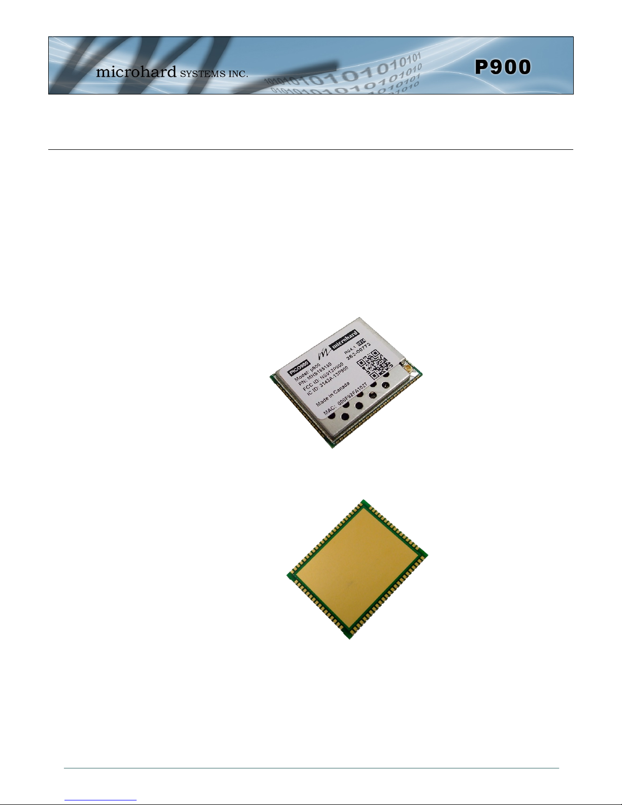
The Pico Series P900 Modem modules are available as a low cost OEM module. This OEM
version supplies all the required raw signals to allow the unit to be tightly integrated into
applications to efficiently maximize space and power requirements. The Microhard
development board can provide a convenient evaluation platform to test and design with the
module. (Contact Microhard Systems for details)
Any P900 Series module may be configured as a Primary Coordinator, Secondary
Coordinator, Standby Coordinator or Remote in a Mesh Topology, or a Master, Repeater or
Remote in a PP or PMP Topology. This versatility is very convenient from a ’sparing’
perspective, as well for convenience in becoming familiar and proficient with using the
module: if you are familiar with one unit, you will be familiar with all units.
Image 2-1: Pico P900 Top View
Image 2-2: Pico P900 Bottom View
© Microhard Systems Inc. Confidential 12
Page 13
33
26.5
3.68
2.31
33
3.5
0.80
1.27
1.18
22.35
28.70
30.01
2.16
19.85
1.50
3.41
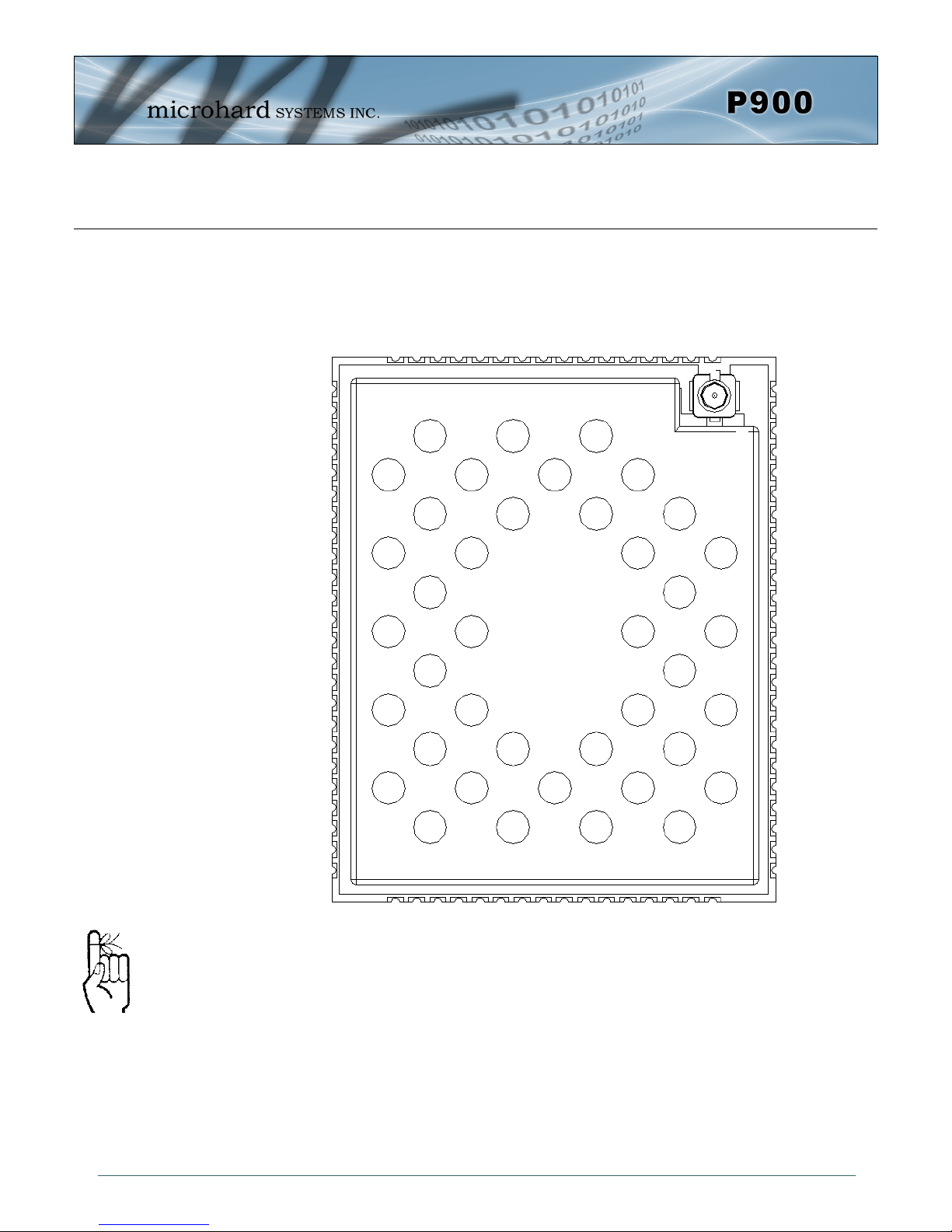
2.0 Hardware Description
2.1 Mechanical Drawings
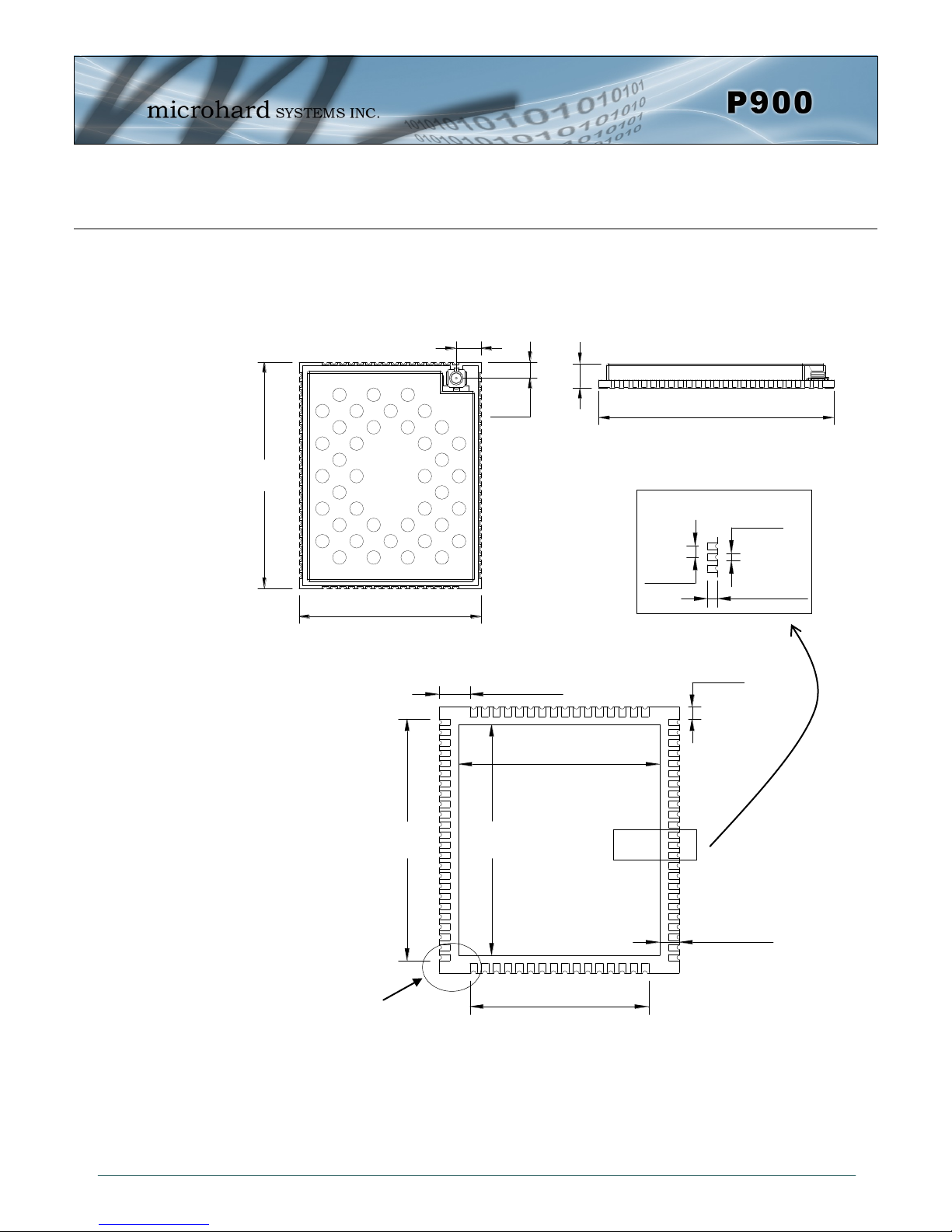
The P900 OEM Modules have an extremely small form factor as seen in Drawing 3-3 below.
(2)
(2)
(A)
Detail
(2)
© Microhard Systems Inc. Confidential 13
See Notes
(2)
Units: millimeters
Ground Plane
Bottom View
Drawing 2-1: P900 OEM Mechanical
(1)
(A)
Detail
1. Ground plane must be connected to GND for required heat dissipation.
2. Due to manufacturing methods additional PCB material may be
present on the corners that cannot be removed. Designs should
allow for a small tolerance of this additional material, ± 0.25mm
Page 14
1.27
0.81
1.83
22.35
30.02
0.99
19.86
28.70
27.99
34.34
2.0 Hardware Description
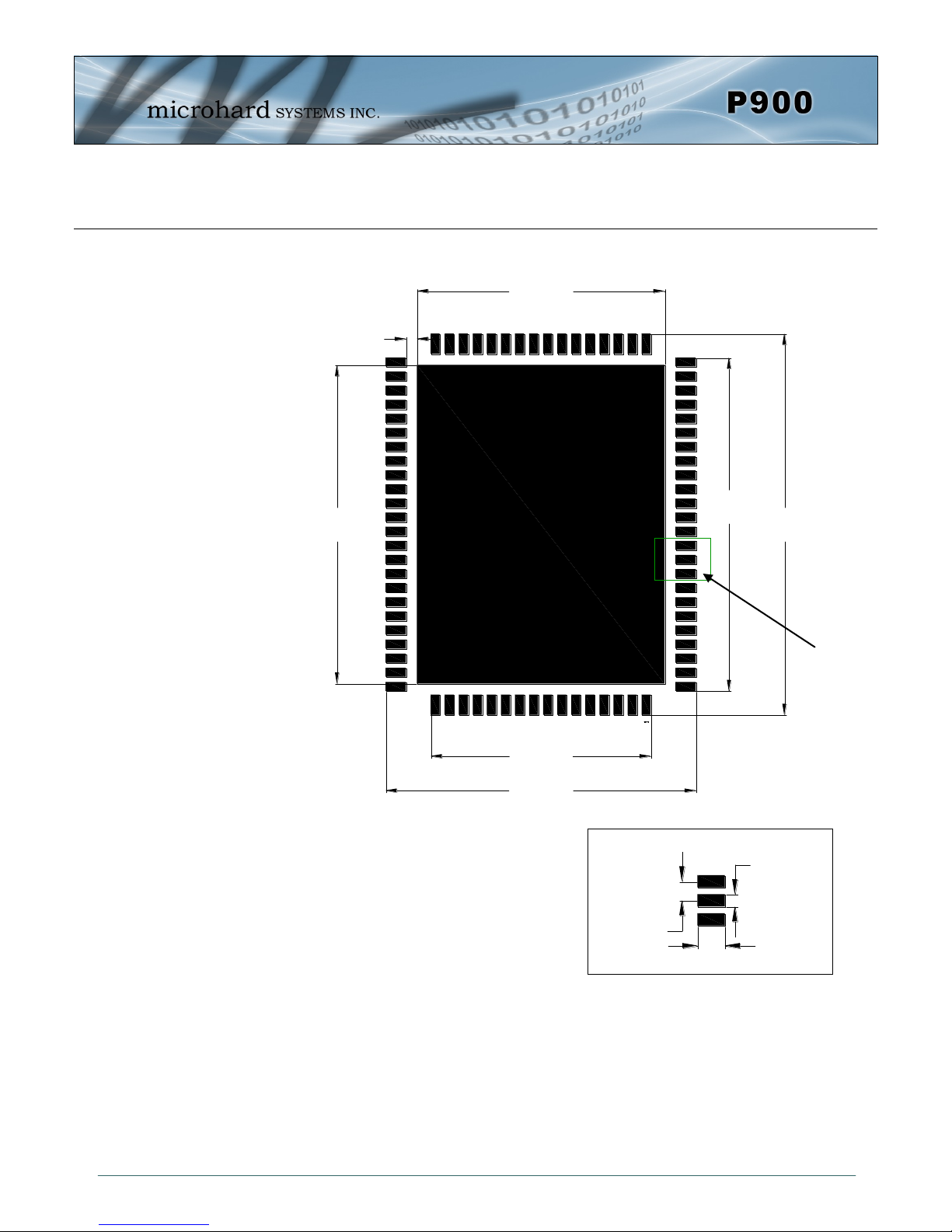
2.1.1 Recommended Solder Mask (Pad Landing)
Units: millimeters
Drawing 2-2: P900 Recommended Solder Mask
Detail
(B)
Detail
(B)
© Microhard Systems Inc. Confidential 14
Page 15
19.91
30.0734.39
28.04
2.18
1.88
2.55
1.27
1.03
0.86
3.50
3.38
4.12
1.00
2.0 Hardware Description
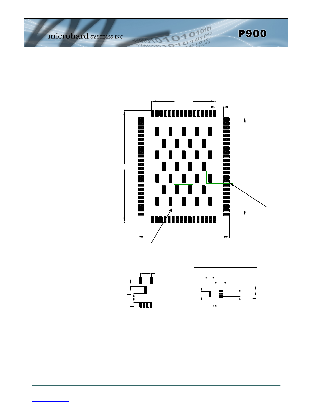
2.1.2 Recommended Solder Paste Pattern
(D)
Detail
Units: millimeters
(D)
Detail
Drawing 2-3: P900 Recommended Solder Paste
2.1.3 OEM Connectors
Antenna
All P900 OEM Modules use an UFL connector for the antenna connection.
Data
The interface to the P900 OEM module is a tight integration using 80 pad SMT connections.
Detail
(C)
Detail
(C)
© Microhard Systems Inc. Confidential 15
Page 16
2.0 Hardware Description
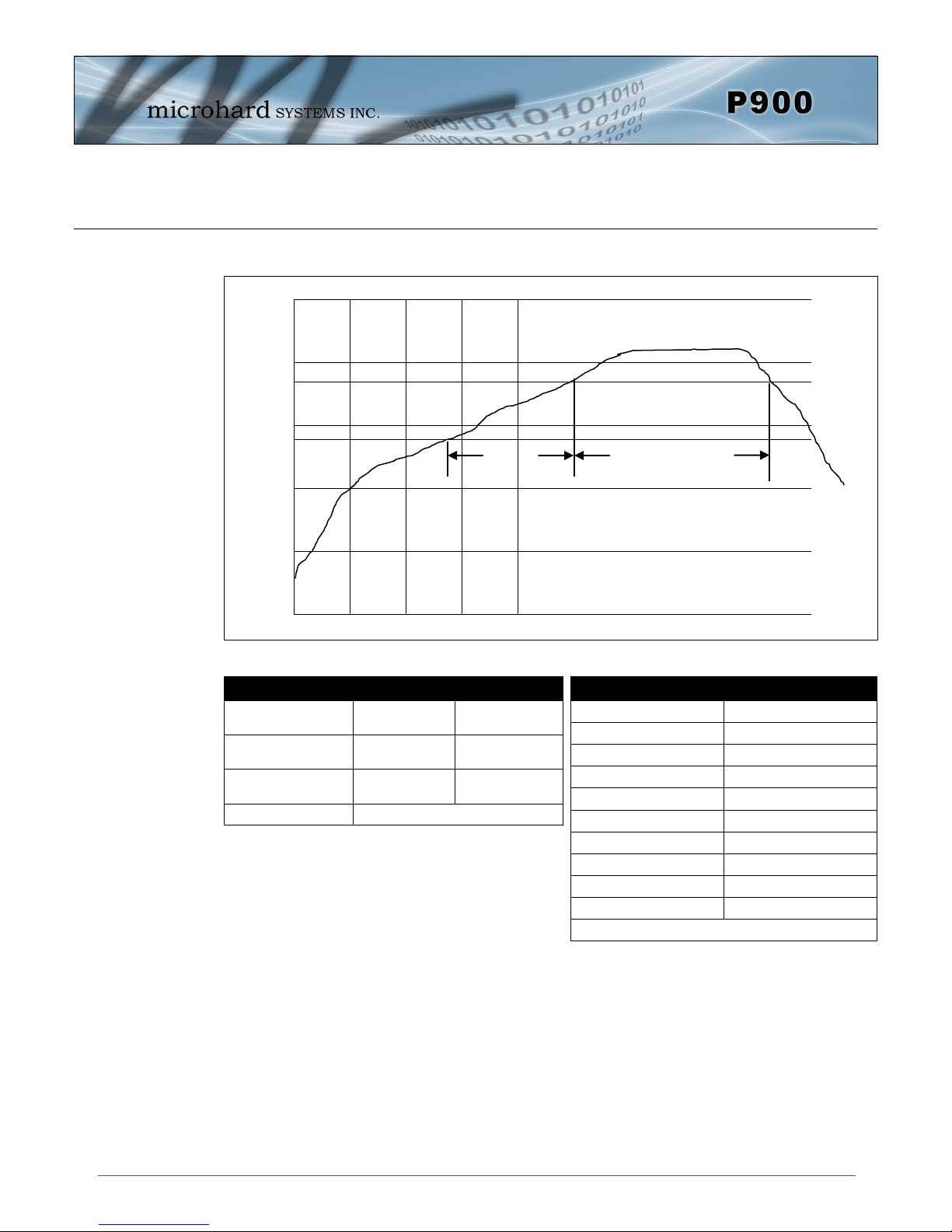
2.1.4 SMT Temperature Profile
300
240
217
180.0
165
T
MAX
=255oC
2.42(oC/s)
60~100s
120.0
60.0
0.0
Drawing 2-4: Reflow Profile
Temperature Zone Time Parameter
Preheat zone:
(40oC - 165oC)
Soak Zone:
(165oC - 217oC)
Reflow zone:
(>217oC)
Cooling zone Cooling rate: 2oC/s ≤ Slope ≤ 5oC/s
Table 2-1: Reflow Parameters
- Heating rate:
60 - 100s -
120s Peak reflow:
0.5oC/s-2oC/s
255oC
120s
Zone Temperature (oC)
1 120
2 140
3 160
4 180
5 215
6 255
7 255
8 255
9 250
10 130
Chain Speed: 60cm/min
Table 2-2: Oven Temperature Profile
2.1.5 SMT Baking Instructions (MSL)
The P900 OEM modules must be baked before mounting, the following baking instruction should be followed for the best results:
a) Minimum of 8 to 12 hours at 125°C +/- 5°C for high-temperature device containers.
b) Unused modules should be stored at ≤ 10% RH
© Microhard Systems Inc. Confidential 16
Page 17
2.0 Hardware Description
2.2 Pico OEM Pin Descriptions
GND
1
GND
DNC
DNC
DNC
DNC
DNC
USR1 - GPS/1PPS
USR2 - Alarm
USR3
I/O1
I/O2
I/O3
I/O4
USR AO0
USR AN0
USR AN1
GND
USBDP
USBDM
RSSI LED1
RSSI LED2
RSSI LED3
LED RX
LED TX
80 79 78 77 76 75 74 73 72 71 70 69 68
2
3
4
5
6
7
8
9
10
11
12
13
14
15
16
17
18
19
20
21
22
23
24
Reserved
Reserved
GND
GND
GND
GND
GND
DNC
DNC
DNC
DNC
DNC
Pico Series
P900
(Top View)
GND
GND
GND
67 66 65
64
Vcc
63
Vcc
62
Vdd
61
Reserved
60
Reserved
59
Reserved
58
Reserved
57
Reserved
56
Reserved
55
Reserved
54
Reserved
53
Reserved
52
Reserved
51
CANRX
50
CANTX
49
Reserved
48
Reserved
47
Wakeup_usr
46
!CONFIG
45
!RESET
44
RSMode
43
Reserved
42
Vbat
41
40 39 38 37 36 35 34 33 32 31 30 29 28 27 26 25
GND
Inputs and outputs are
3.3V nominal (3.0V min
— 3.6V max) unless
otherwise specified.
The above drawing depicts a top view of the P900-OEM Module. The corner pads (1, 25, 41,
and 65) are printed directly on the bottom of the PCB for easy identification.
A full description of the connections and function of each pin is provided on the pages that
follow.
© Microhard Systems Inc. Confidential 17
Reserved
GND
GND
Serial RING
Serial RxD
Serial TxD
Serial DSR
Serial CTS
Serial DTR
Serial DCD
Serial RTS
Control RxD
USR SCK
Control TxD
Drawing 2-5: Pico P900 80-pin OEM Connection Info
GND
GND
Page 18

2.0 Hardware Description
Caution: During power up
or reset, output pins from
the Pico are in an unknown
state. It is advised to use
pull up or pull down
resisters as appropriate.
Pin Name No. Description
GND 1,17,25-26,39-
DNC 2,3,4,5,6 Reserved for factory use only.
USR1 –
GPS/1PPS
USR2 - Alarm 8
USR3 9
I/O 1,2 10,11 Digital Outputs. 3.3 V Output @ 3mA maximum. O
I/O3,4 12,13 Future Use I/O
USR_ANO0 14
USR_AN0
USR_AN1
USBDP 18
USBDM 19
LED_1 (RSSI1) 20 Receive Signal Strength Indicator 1. Active high, cannot drive LED
LED_2 (RSSI2) 21 Receive Signal Strength Indicator 2. Active high, cannot drive LED
LED_3 (RSSI3)
LED_RX 23 Active high output indicates receive and synchronization status.
LED_TX 24 Active high output indicates module is transmitting data over the RF
Serial RING 27
Serial RxD 28 Receive Data. Logic level input into the modem. It is recommended
Serial TxD 29 Transmit Data. Logic level Output from the modem. It is
Serial DSR 30
Serial CTS 31
Serial DTR 32 Data Terminal Ready. Active low input. I
Serial DCD 33 Data Carrier Detect. Active low output. O
Serial RTS 34 Request To Send. Active low input. I
USR SCK 35
41,65-67,75-80
Ground reference for logic, radio, and I/O pins.
*Currently Not Supported. For Future Expansion*
7
*Reserved for future use.*
*Reserved for future use.*
*Currently Not Supported. For Future Expansion*
15
Analog Inputs. 0 to 3V input, 12 bit. I
16
*Currently Not Supported. For Future Expansion*
*Currently Not Supported. For Future Expansion*
directly. Requires current limiting resistor. 8mA maximum.
directly. Requires current limiting resistor. 8mA maximum.
22
Receive Signal Strength Indicator 3. Active high, cannot drive LED
directly. Requires current limiting resistor. 8mA maximum.
Active high, cannot drive LED directly. Requires current limiting
resistor. 8mA maximum.
channel. Active high, cannot drive LED directly. Requires current
limiting resistor. 8mA maximum.
Internally connected to GND through a 22kΩ resistor. In RS485
modes the RING line is set high and is normally used to enable the
receiver of the RS485 driver.
to wire this pin out through a zero ohm resister to a header and
jumper block for external access to the serial port for modem
recovery procedures.
recommended to wire this pin out through a zero ohm resister to a
header and jumper block for external access to the serial port for
modem recovery procedures.
Data Set Ready. Active low output. The DSR line may be used to
enable the transmitter of the RS485 driver chip.
Clear To Send. Active low output. The CTS line may be used to
enable the transmitter of the RS485 driver chip.
*Currently Not Supported. For Future Expansion*
Dir
I
O
O
O
O
O
O
O
O
O
I
O
O
O
I
© Microhard Systems Inc. Confidential 18
Table 2-3: Pico Series Pin Description
Page 19
2.0 Hardware Description
Caution: During power up
or reset, output pins from
the Pico are in an unknown
state. It is advised to use
pull up or pull down
resisters as appropriate.
Pin Name No. Description
Reserved 36
Control RxD 37 Diagnostics receive data. Logic level input from a PC to the module. I
Control TxD 38 Diagnostics transmit data. Logic level output from module to a PC. O
Vbat 42 Input voltage sensing analog input line, up to 60VDC maximum. Used to
Reserved 43
RSMode 44
!RESET 45 Active low input will reset the module. I
!CONFIG 46 Active low input signal to put module into default serial interface (RS232) and
!Wakeup_usr 47 Active high input used to wake the model from sleep mode. I
Reserved 48
Reserved 49
CANTX 50
CANRX 51
Reserved 52-61
Vdd 62 Positive voltage supply voltage for the digital section of the module (3.3V). I
Vcc 63,64 Positive voltage supply voltage for the radio module (3.3V). The Vcc lines are
Reserved 68,69
DNC 70-74 Reserved for factory use only.
*Reserved for future use.*
measure the main supply voltage. User design must add a 10kΩ 1% 1/16W
resistor in series.
*Reserved for future use.*
Internally connected to GND through a 10kΩ resistor. *Reserved for future
use.*
default baud rate (9600/8/N/1) during power up. Pull high or leave floating.
*Reserved for future use.*
*Reserved for future use.*
*Currently Not Supported. For Future Expansion*
*Currently Not Supported. For Future Expansion*
*Reserved for future use.*
internally connected together.
*Reserved for future use.*
Table 2-3: Pico Series Pin Description (continued)
Dir
O
I
I
I
All serial communications signals are logic level (0 and 3.3V). DO NOT connect RS-232 level
(+12, -12VDC) signals to these lines without shifting the signals to logic levels.
© Microhard Systems Inc. Confidential 19
Page 20

2.0 Hardware Description
2.3 Minimum Connection Requirements
3.3V
62 63 64
VCC
VDD
Antenna
UFL
Optional
RS-232
Driver
29 Serial TxD
28 Serial RxD
P900
GND Pins
1 17 25 26 39 40 41 65 66 67 78 79 80
© Microhard Systems Inc. Confidential 20
Drawing 2-6: P900 Minimum Connection Block Diagram
Page 21
2.0 Hardware Description
2.4 Electrical Characteristics
2.4.1 Test Conditions
Unless otherwise specified, all voltages are referenced to Vss(GND).
2.4.1 Minimum and Maximum Values
Unless otherwise specified the minimum and maximum values are guaranteed in the worst
conditions of ambient temperature, supply voltage and frequencies.
Data based on characterization results, design simulation and/or technology characteristics
are indicated in the table footnotes and are not tested in production. Based on
characterization, the minimum and maximum values refer to sample tests and represent the
mean value plus or minus three times the standard deviation (mean±3Σ).
2.4.1.2 Typical Values
Unless otherwise specified, typical data are based on TA = 25 °C, VDD = 3.3 V. They are given
only as design guidelines and are not tested.
Typical ADC accuracy values are determined by characterization of a batch of samples from
a standard diffusion lot over the full temperature range, where 95% of the devices have an
error less than or equal to the value indicated (mean±2Σ).
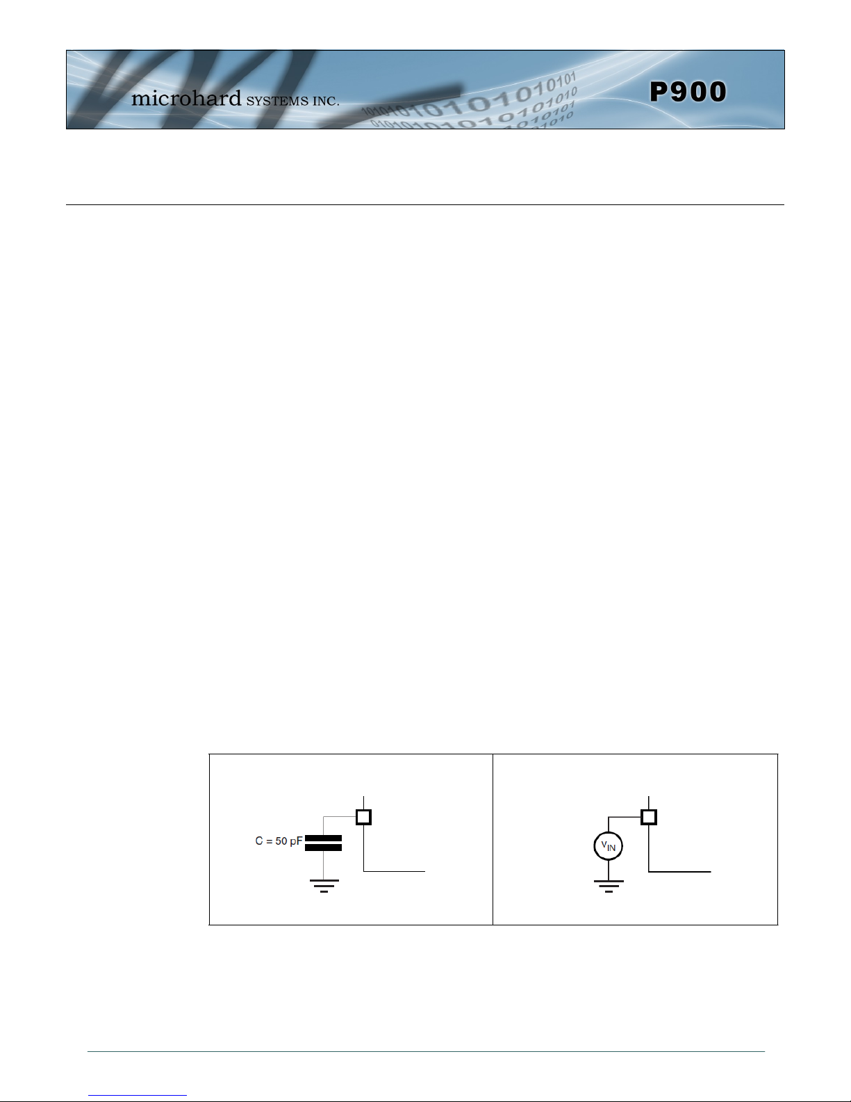
2.4.1.3 Loading Capacitor
The loading conditions used for pin parameter measurement are shown in Figure 2-1.
2.4.1.4 Pin Input Voltage
The input voltage measurement on a pin of the Pico is described in Figure 2-2.
Figure 2-1 Pin Loading Conditions
© Microhard Systems Inc. Confidential 21
Pico pin
Figure 2-2 Pin Input Voltage
Pico pin
Page 22

2.0 Hardware Description
2.4.2 Absolute Maximum Ratings
Stresses above the absolute maximum ratings listed in Table 2-2: Voltage Characteristics
and Table 2-3: Current Characteristics may cause permanent damage to the device. These
are stress ratings only and functional operation of the device at these conditions is not
implied. Exposure to maximum rating conditions for extended periods may affect device
reliability.
Symbol Ratings Min Max Unit
VCC/VDD External main supply voltage. 0 3.8
VIN Input voltage on any pin. -0.3 VDD+0.3
V
Table 2-4 Voltage Characteristics
Symbol Ratings Max Unit
I
Total current into Pico Series (source). 70
VDD
I
Total current out of Pico Series (sink). 70
VSS
I
Output current sunk by any I/O and control pin. 20
IO
Output Current sourced by any I/O and control pin. -8
Table 2-5 Current Characteristics
mA
2.4.3 Operating Conditions
2.4.3.1 Operating Conditions at Power-up / Power-down
The parameters given in Table 2-4: Operating Conditions at Power-up/ Power-down are
derived from tests performed under the ambient temperature ratings of the Pico Series.
Symbol Parameter Min Max Unit
VDD
VDD rise time rate. 0 ∞
VDD fall time rate. 20 ∞
Table 2-6 Operating Conditions at Power-up/Power-down
µs/V t
2.4.3.2 Operating Conditions Voltage Characteristics
The parameters given in Table 2-5: Operating Conditions Voltage Characteristics are
derived from tests performed under the ambient temperature ratings of the Pico Series.
Symbol Ratings Min Max Unit
VCC External radio supply voltage. 3.3
VDD External digital supply voltage. 3.0 3.6
1. The modem will not be able to transit at full power if V
© Microhard Systems Inc. Confidential 22
(1)
3.6
Table 2-7 Operating Conditions Voltage Characteristics
is less than 3.3VDC.
CC
V
Page 23
2.0 Hardware Description
2.4.3.3 Operating Conditions Current Characteristics
The parameters given in Table 2-6: Operating Conditions Current Characteristics are
derived from tests performed under the ambient temperature ratings of the Pico Series. Test
conditions measured while Vcc = 3.3V, VDD = 3.3V, Frequency 915MHz and ambient
temperature of 25oC.
Symbol Ratings Min Typ Max Unit
I
Radio current 100% TX @ 1W 1250 1500
VCC(TX)
I
Radio current 100% TX @ 500mW 375 500
VCC(TX)
I
Radio current 100% TX @ 100mW 180 250
VCC(TX)
I
Radio current 100% RX @ 1W 75 100
VCC(RX)
I
VCC(RX-RUN)
I
VCC(IDLE)
I
VDD(RUN)
I
VDD(IDLE)
Radio RX running 40 75
Radio Idle current 2.5 3.5
Digital current 45 50
Digital idle current 5
mA
Table 2-8 Operating Conditions Current Characteristics
2.4.3.4 I/O Port Characteristics
General Input / Output Characteristics
The parameters given in Table 2-7: I/O Static Characteristics are derived from tests
performed under the ambient temperature ratings of the Pico Series. All I/Os are CMOS and
TTL compliant. I/O’s refer to all input and outputs of the Pico Series.
Symbol Parameter Conditions Min Typ Max Unit
VIL
VIH
VIL
VIH
V
I
RPU
RPD
CIO
1. Hysteresis voltage between Schmitt trigger switching levels. Based on characterization, not tested in production.
2. Pull-up and pull-down resistors can be used on input/output pins.
Input low level voltage
Input high level voltage 2 VDD+0.5
Input low level voltage
Input high level voltage 0.65 VDD VDD+0.5
IO Schmitt trigger voltage
hys
hysteresis
Input leakage current
lkg
Weak pull-up equivalent resistor
Weak pull-down equivalent resistor
I/O pin capacitance
(1)
(2)
Table 2-9 I/O Static Characteristics
VSS ≤ VIN≤ VDD
(2)
TTL ports
CMOS ports
VIN = VSS
VIN = VDD
-0.5 0.8
-0.5 0.35 VDD
200
±1
30 40 50
30 40 50
8
V
V
mV
µA
kΩ
pF
© Microhard Systems Inc. Confidential 23
Page 24
2.0 Hardware Description
Output Driving Current
The GPIOs (general purpose input/outputs) can sink or source up to +/-8 mA, and sink
+20 mA (with a relaxed VOL).
In the user application, the number of I/O pins which can drive current must be limited to
respect the absolute maximum rating specified in Section 2.5.2:
● The sum of the currents sourced by all the I/Os on VDD cannot exceed the absolute maximum rating
I
(see Table 2-3).
VDD
The sum of the currents sunk by all the I/Os on VSS cannot exceed the absolute maximum rating I
(see Table 2-3).
Output Voltage Levels
Unless otherwise specified, the parameters given in Table 2-8 are derived from tests
performed under ambient temperature and VDD supply voltage ratings of the Pico Series. All I/Os are
CMOS and TTL compliant.
VSS
Symbol Parameter Conditions Min Max Unit
Output low level voltage for an I/O pin
(1)
V
OL
V
OH
V
OL
V
OH
V
OL
V
OH
1. The IIO current sunk by the device must always respect the absolute maximum rating specified in Table 2-3 and the sum of IIO (I/O ports and control
2. The IIO current sourced by the device must always respect the absolute maximum rating specified in Table 2-3 and the sum of IIO (I/O ports and
3. Based on characterization data, not tested in production.
when 8 pins are sunk at same time
Output high level voltage f or an I/O pin
(2)
when 8 pins are sourced at same time
Output low level voltage for an I/O pin
(1)
when 8 pins are sunk at same time
Output high level voltage f or an I/O pin
(2)
when 8 pins are sourced at same time
Output low level voltage for an I/O pin
(1)(3)
when 8 pins are sunk at same time
Output high level voltage f or an I/O pin
(2)(3)
when 8 pins are sourced at same time
pins) must not exceed I
control pins) must not exceed I
.
VSS
.
VDD
Table 2-10 Output Voltage Characteristics
TTL port
IIO = +8mA
CMOS port
IIO = +8mA
IIO = +20mA
0.4
V
VDD-0.4
0.4
V
2.4
1.3
V
VDD-1.3
Input / Output AC Characteristics
The values of input/output AC characteristics are given in Table 2-9.
Symbol Parameter Conditions Min Max Unit
t
Output high to low f all time
f(IO)out
t
Output low to high level rise time 125
r(IO)out
t
EXTlpw
Pulse width of external signals used as
interrupts.
CL = 50 pF
1 ms
125
ns
© Microhard Systems Inc. Confidential 24
Table 2-11 Input / Output AC Characteristics
Page 25
2.0 Hardware Description
NRST Pin Characteristics
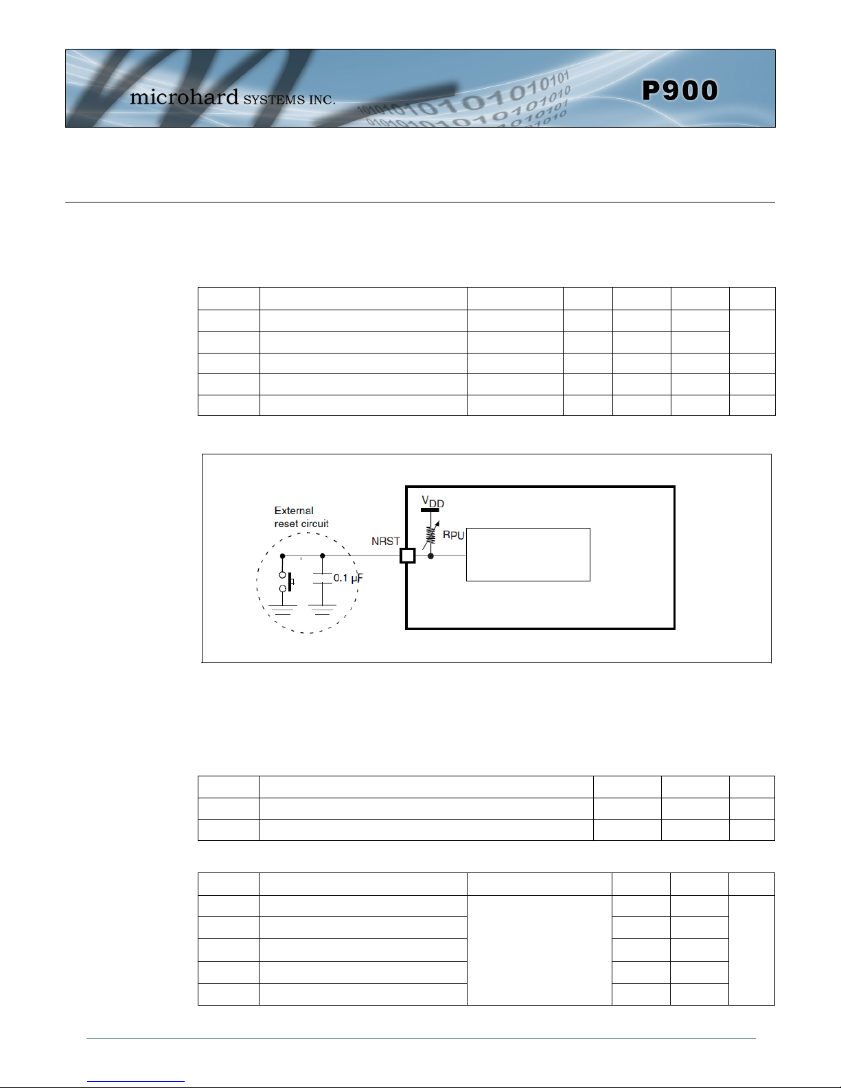
The NRST pin input driver uses CMOS technology. It is connected to a permanent pull-up
resistor, RPU (see Table 2-7).
Symbol Parameter Conditions Min Max Unit Typ
V
NRST Input low level voltage -0.5 0.7
IL(NRST)
V
IH(NRST)
V
hys(NRST)
RPU Weak pull-up equivalent resistor VIN=VSS 30 50 kΩ 40
VNF NRST Input pulse 300 ns
NRST Input high level voltage
NRST Schmitt trigger voltage hysteresis mV 200
Table 2-12 NRST Pin Characteristics
2 VDD+0.5
V
Pico Series
Figure 2-3 Recommended NRST Pin Protection
2.4.3.5 12-bit ADC Characteristics
The parameters given in Table 2-11: ADC Characteristics are derived from tests performed
under the ambient temperature and supply voltage ratings of the Pico Series.
Symbol Parameter Min Max Unit
V
Conversion voltage range 0 3.0 V
AIN
R
Symbol Parameter Test Conditions Typ Max Unit
ET
EO
EG
ED
EL
External input impedance
AIN
Total unadjusted error
Offset error
Gain error
Differential linearity error
Integral linearity error
Table 2-13 12-bit ADC Characteristics
Table 2-14 ADC Accuracy
0 1.2 kΩ
1.3 2
1 1.5
0.5 1.5
0.7 1
0.8 1.5
LSB TA = 25OC
© Microhard Systems Inc. Confidential 25
Page 26

2.0 Hardware Description
ADC Accuracy Characteristics
[1LSB
= 3.0/4096]
IDEAL
Figure 2-4 ADC Accuracy Characteristics
© Microhard Systems Inc. Confidential 26
Page 27
2.0 Hardware Description
2.5 P900 to Nano n920 Pin-Outs
The following table shows a pin-out comparison between the P900 and the n920. This table
may be useful for customers who current have the n920 who wish to migrate to the P900
platform.
Pin Name P900 Pin No. n920 Pin No. Description
USR1 7 35
USR2 8 37
USR3 9 39
USR_AN0 15 9
USBDP 18 25
USBDM 19 21
LED_1 (RSSI1) 20 30 Rec eive Signal Strength Indicator 1.
LED_2 (RSSI2) 21 28 Rec eive Signal Strength Indicator 2.
LED_3 (RSSI3)
For detailed pin
descriptions refer to
Section 2.3 Pin Description.
LED_RX 23 22 Active high output indicates receive and synchronization status.
LED_TX 24 24 Active high output indicates module is transmitting RF data.
Serial RING 27 38
Serial RxD 28 42 Receive Data. Logic level input into the modem.
Serial TxD 29 44 Transmit Data. Logic level Output from the modem.
Serial DSR 30 36 Data Set Ready. Active low output.
Serial CTS 31 32 Clear To Send. Active low output.
Serial DTR 32 40 Data Terminal Ready. Active low input.
Serial DCD 33 46 Data Carrier Detect. Active low output.
Serial RTS 34 34 Request To Send. Active low input.
USR SCK 35 50
Control RxD 37 20 Diagnostics receive data.
Control TxD 38 18 Diagnostics transmit data.
Vbat 42 17 Battery Voltage sensing analog input line.
RSMode 44 19
!RESET 45 15 Active low input will reset the module.
!CONFIG 46 13 A ctive low input signal to put module into default serial mode.
Wakeup_usr 47 11 Active high input used to wake the model from sleep mode.
!Bootpgm_mode 48 7
CANTX 50 12
CANRX 51 10
Vdd 62 Positive voltage supply voltage for the digital section of the module (3.3V).
Vcc 63,64 Positive voltage supply voltage for the radio module (3.3V).
Vcc2 75,76,77 N/A
*Currently Not Supported. For Future Expansion*
*Reserved for future use.*
*Reserved for future use.*
Analog Input 0. *Future Use.*
*Currently Not Supported. For Future Expansion*
*Currently Not Supported. For Future Expansion*
22 26
51,53,55,57,59
Receive Signal Strength Indicator 3.
*Reserved for future use.*
*Currently Not Supported. For Future Expansion*
*Reserved for future use.*
*Reserved for future use.*
*Currently Not Supported. For Future Expansion*
*Currently Not Supported. For Future Expansion*
*Reserved for future use.*
Table 2-15: P900 to Nano n920 Pin Description
© Microhard Systems Inc. Confidential 27
Page 28

2.0 Hardware Description
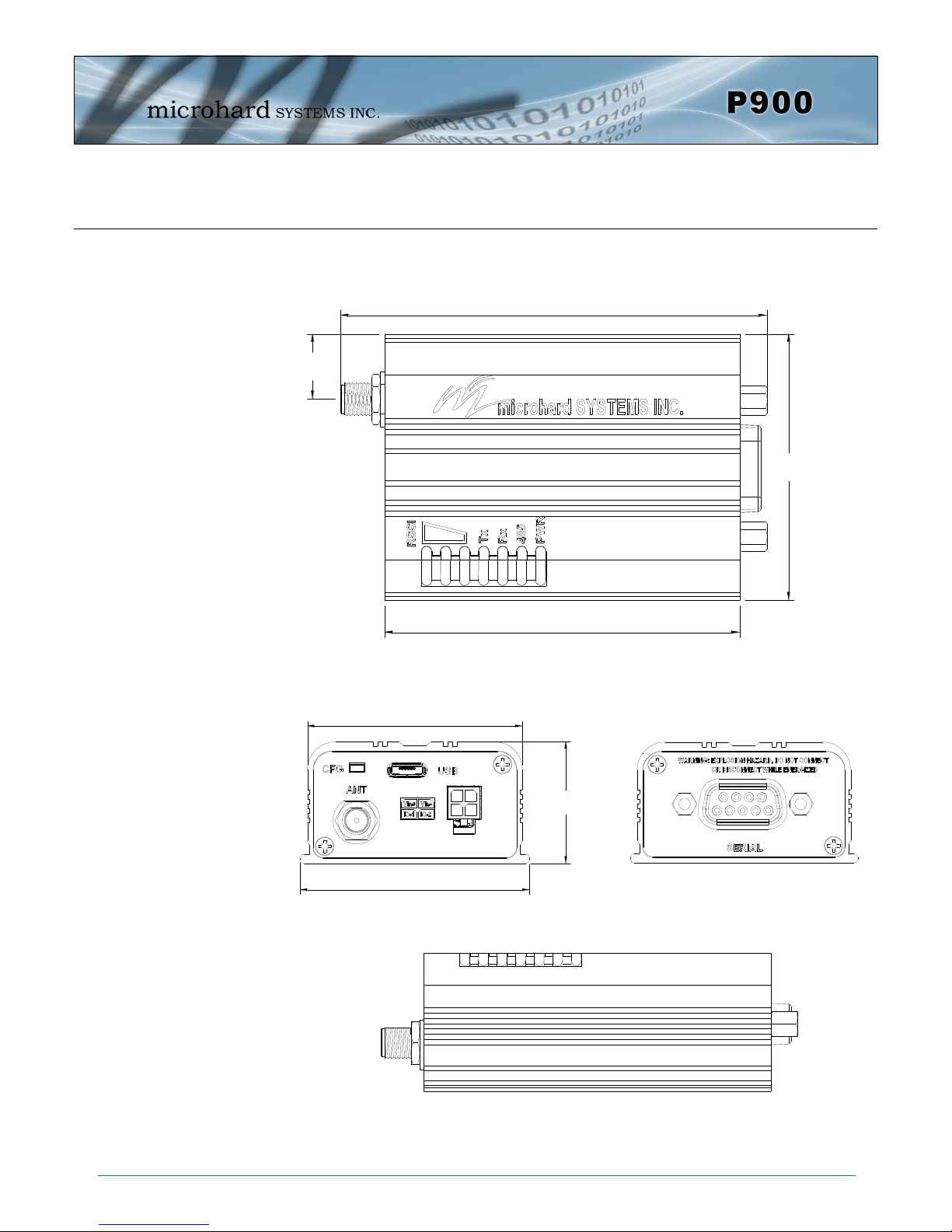
2.6 P900 Enclosed
The Pico Enclosed provides a standalone P900 with standard interfaces for Data, Power and
Antennas. The P900 Enclosed is ideal for base stations or applications where complicated
integration of the OEM module is not required, but a modem with a small footprint is still
required. The P900 Enclosed can also be used to quickly evaluate the features and
performance of the P900 modems.
The P900 Enclosed provides quick access to several of the interfaces of the P900, such as:
Input Power (9-30VDC)
Power LED (Blue)
RS232/RS485 Data Interface
RSSI LED Indicators (Green)
TX/RX LED Indicators (Red/Green)
CONFIG Button
Antenna
USB Port (Diagnostic Port)
I/O pins (Future Development)
© Microhard Systems Inc. Confidential 28
Image 2-4: P900 Enclosed
Page 29
65.40
78.48
49.00
12.00
46.00
26.00
49.00
2.0 Hardware Description
2.6.1 P900 Enclosed Dimensional Drawings
Drawing 2-7: P900 Top View
Drawing 2-8: P900 Enclosed End Views
© Microhard Systems Inc. Confidential 29
Drawing 2-9: P900 Enclosed Side View
Notes: The dimension unit is mm.
Page 30
12.5
12.5
20.1
23.7
4.0
4.0
12.2
17.2
65.2
47.4
45.0
30.0
54.0
20.1
2.0 Hardware Description
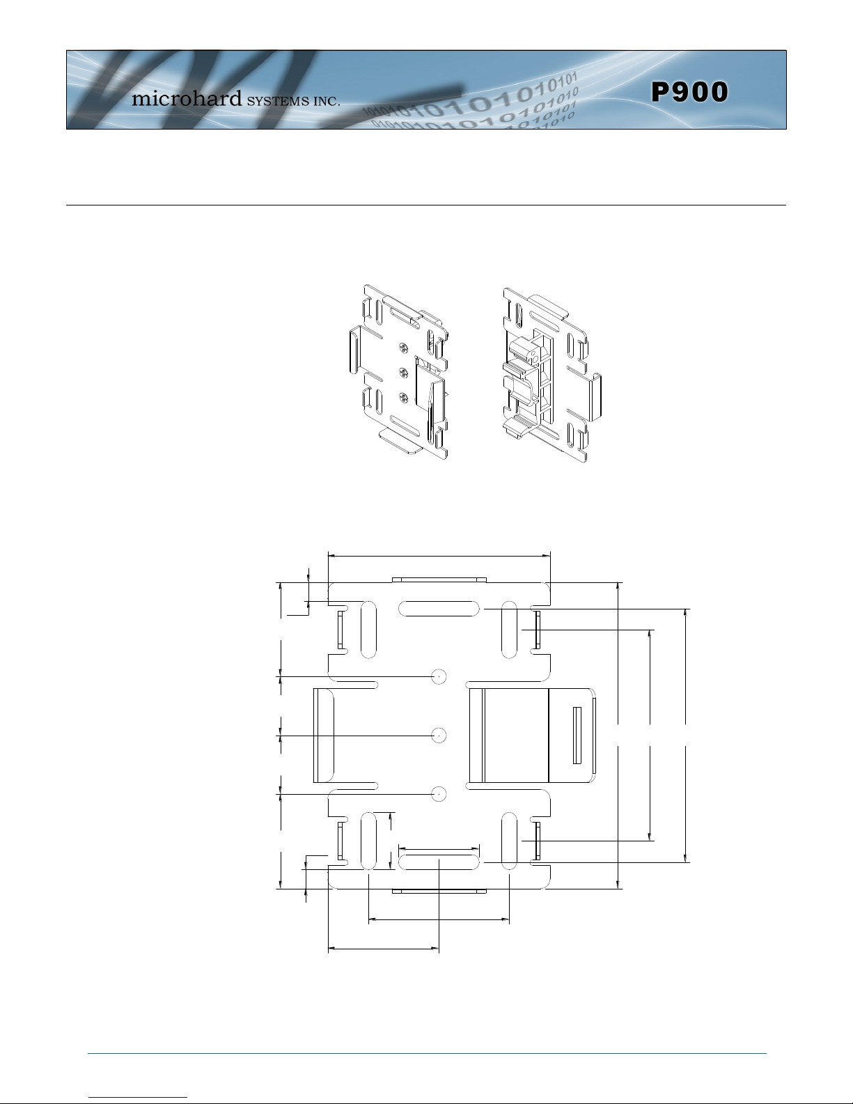
2.6.2 P900 Enclosed Mounting Bracket (Order Option)
Drawing 2-10: P900 –ENC Mounting Bracket Front/Rear (Shown optional TS35 DIN Rail Mount)
© Microhard Systems Inc. Confidential 30
Drawing 2-11: P900 –ENC Mounting Bracket Top View
Notes: The dimension unit is mm.
Page 31

2.0 Hardware Description
2.6.3 P900 Enclosed Connectors & LED Indicators
Drawing 2-12: Connectors & LED’s (Top & End)
PWR (Blue)
This LED will illuminate when the P900 Enclosed is connected to a power source (9-30 VDC)
485 (Blue)
This LED will illuminate when the P900 Enclosed Data port is configured as a RS485 port.
(Register S142 Serial Channel Mode set to RS485 and Handshaking set to &K1)
TX LED (Red)
When illuminated, this LED indicates that the modem is transmitting data over the air.
RX LED (Green)
This LED indicates that the modem is synchronized and has received valid packets.
Receive Signal Strength Indicator (RSSI) (3x Green)
As the received signal strength increases, starting with the furthest left, the number of active
RSSI LEDs increases. Signal strength is calculated based on the last four valid received
packets with correct CRC. The value of RSSI is reported in S123.
MODE Unit Type
COMMAND All OFF OFF OFF
DATA P.Coordinator
DATA - during sync.
acquisition
DATA - when
synchronized
S.Coordinator
S.Coordinator
Remote/
Standby
S.Coordinator
Remotes/
Standby
RX/SYNC TX RSSI 1,2,3
ON while receiving valid
data
OFF OFF Cycling with 300ms ON time
ON while synced ON when
LED STATUS
ON while
Transmitting data
transmitting
1-3 ON in proportion to signal
strength received from remotes.
1-3 ON in proportion to signal
strength received from Coordinator
© Microhard Systems Inc. Confidential 31
Table 2-16: LED Operation
Page 32

Vin+
Vin-
IO-1
IO-2
2.0 Hardware Description
CFG Button
Holding this button while powering-up the modem will boot the unit into COMMAND mode:
the default serial interface will be active and temporarily set to operate at its default serial
settings of RS232 and 9600/8/N/1.
USB
Micro-AB USB Port. Internal USB to Serial Converter.
Provides access to the Serial Diagnostics Port.
The SERIAL (RS232/485 Port (DCE)) on the
Enclosed model is for:
RS232/485 Serial data when in DATA
MODE, or
for configuring the modem when in
COMMAND MODE.
Vin+/Vin– is used to power the unit. The input Voltage
range is 9-30 Vdc.
IO-1 / IO-2
Programmable I/O. Not currently supported in firmware.
Future Development.
ANT
RP-SMA Female Bulkhead Antenna connector.
Caution: Using a
power supply that
does not provide
proper voltage may
damage the modem.
Drawing 2-13: Connectors & LED’s (Front & Back)
Pin
No.
1 DCD
2 RXD TX- Data-
3 TXD RX+
4 DTR
5 Ground
6 DSR
7 RTS RX-
8 CTS TX+ Data+
9 N/C
Table 2-17: Data DB9 Pin Assignments
RS232
RS485
Full-Dup
RS485
Half-Dup
© Microhard Systems Inc. Confidential 32
Page 33

3.0 Mesh Configuration
To begin configuration, the P900 must be mounted into a either a Microhard supplied development board (with factory attached interface card), or be mounted into a customer designed
platform. The P900 is configured using AT commands through the Data port, or using special
diagnostic commands through the Diagnostic Port. Refer to Section 2: Hardware Descrip-
tion for information related to interfacing to, or powering the module.
To issue AT commands through the Data port, the P900 must first be set into Command
Mode as described below.
3.1 Configuration/Unit Modes
3.1.1 Command Mode
the P900 module is offline (data is not passing through the unit via it’s local data lines
or RF communications)
if installed in a Development Board, the only LED illuminated will be the blue power
LED.
the P900’s configuration options (registers) may be viewed and modified using AT
commands.
Two methods are typically used to place the Pico Series into Command Mode.
1. Force to Command Mode
Power down off the Development Board assembly.
Connect a 9-pin straight-through serial cable from the PC serial port to the rear RS-
232 port (DATA) of the modem.
Launch a terminal communications program (e.g. HyperTerminal) and configure for
9600 bps, 8 data bits, No parity, 1 stop bit (8N1), no flow control
press and hold the CONFIG button
continue to press the CONFIG button and apply power to the modem
release the CONFIG button
On power up the terminal session window should show “NO CARRIER OK” as seen
below:
the P900 is now in command mode, and AT commands can be used to configure or
query the settings. AT&V will display the current configuration, and the registers can
be queried using the ATSXXX=? Command where XXX = the register number. Help is
available using the ATSXXX /? Command.
Any and all changes must be written to NVRAM using the AT&W command.
Image 3-1: Command Mode
© Microhard Systems Inc. Confidential 33
Page 34

3.0 Mesh Configuration
2. Escape from Data Mode
With the P900 powered up and ‘online’, connect a 9-pin straight-through serial cable
from the PC serial port to the RS-232 DATA port on the dev board.
Launch a terminal program (e.g. HyperTerminal) and configure for the P900’s estab-
lished serial baud rate parameters (PC & modem must match).
Pause 1 second, type ‘+++’ , pause 1 second: the monitor should show the module
response of ‘NO CARRIER OK’
The P900 is now in command mode, and AT commands can be used to configure or
query the settings.
Entering the AT&V command as shown will show the current configuration as seen
below: (The data displayed varies based on network and unit type.)
3.1.2 Data Mode
Data Mode is the normal operational state of all deployed P900 modules. In this mode the module is
prepared to exchange data as per its configuration settings. Available LED indications can provide an
indication of the data exchange (TX and RX LEDs).
To enter DATA mode from COMMAND mode, enter the command: ATA [Enter]
Image 3-2: Command Mode
Image 3-3: Command Mode - AT&V Display
© Microhard Systems Inc. Confidential 34
Page 35

3.0 Mesh Configuration
3.2 Mesh Network
In a Mesh Network Topology, radios can communicate with each other directly or, if required, through
another mesh node. In traditional Point to Multipoint (PMP) and Point to Point (PP or PTP) network topologies a Master is used to not only keep the network synchronized in frequency and time
(synchronization), but all data is also routed through the Master. Using Mesh, data can be sent directly
between devices without the need to route all data through a single unit, which, when offline, brings
down the entire network.
In situations where a direct path is not available between source and destination units, routing can be
enabled to find and provide route information to ensure that data is delivered to the required destination.
A Mesh network can be designed in such a way that redundant paths are available for data transfer,
unknown routes can be auto discovered, and the best path is used to reach the intended destination. If
a path or route changes due to a unit going offline, or moving such as in a mobile application, the network can heal itself by finding a new path to the destination. All this is done without data being routed
through a single point as seen in traditional PMP and P2P networks. Routing features can be enabled
on any unit, coordinators or remotes. Enabling routing on multiple units provides the greatest redundancy, eliminating the risk of any single point of failure.
Any frequency hopping network, even a Mesh Network requires that at least one unit be tasked with the
job (primary coordinator) of making sure all units in the network are hopping at the same time, on the
same frequency. This is accomplished by sending out synchronization data for all units to hear. If the
network grows, or additional coverage is required, additional units can also be tasked with the job of
synchronization (secondary coordinators).
As seen in the illustration below, there are many paths that data could take to each any destination in a
Mesh network. Mesh Networking generally results in achieving extensive network redundancy. Mesh is
enabled by setting register S133 to 2 or 3 (for Mesh with Roaming) (ATS133=2 or ATS133=3, Network
Type).
Mesh
Mesh
Mesh
Mesh
Mesh
© Microhard Systems Inc. Confidential 35
Mesh
Drawing 3-1: Mesh Network Topology
Mesh
Page 36

3.0 Mesh Configuration
3.2.1 Operating Modes / Unit Types
In a Microhard Mesh Network, there are four unit types or operating modes that are available: the Primary Coordinator, the Secondary Coordinator, the Standby Coordinator, and the Remote. Any P900
module can be configured to perform any of these roles, the paragraphs and diagrams that follow attempt to describe the purpose of each unit.
The Primary Coordinator’s role is to provide network synchronization for the system, which ensures all
units are active and able to communicate as required. In any Mesh Network, there can only be a single
Primary Coordinator. Additional coordinators can be deployed for redundancy and/or, to extended network coverage to areas not serviced by the Primary Coordinator. For any units to be able to communication in a Mesh Network, they must be able to hear synchronization data from a coordinator.
What if the Primary Coordinator goes offline or fails? A second unit, called a Standby Coordinator can
be deployed to monitor the network synchronization level, and take over the duties of the Primary Coordinator should it ever fail. For this reason the primary coordinator should not be used to interface with an
end device, but rather left to perform the duties of network synchronization. If used to interface with an
end device, and it fails, the Standby Coordinator will have a unique units address, different from that of
the Primary Coordinator. Any data that was destined for the Primary Coordinator will not automatically
be routed to the Standby Coordinator.
Although routing can be enabled on a Primary Coordinator, data is not automatically routed through the
Primary, or any other coordinator for that matter. This is mentioned to stress that the role of a coordinator of any type is to simply keep the network synchronized in time and frequency.
The diagram below shows a unit configured as a Primary Coordinator. Any other mesh unit that can
hear the Primary Coordinator can participate in a Mesh Network.
Primary
Coordinator
Mesh
© Microhard Systems Inc. Confidential 36
P.C.
Mesh
Drawing 3-2: Primary Coordinator
Mesh
Page 37

3.0 Mesh Configuration
Secondary Coordinators are used to extend the coverage of the Primary Coordinator. More than one
Secondary Coordinator can be used for redundancy or to ensure adequate network coverage. A Secondary Coordinator must be able to communicate with the Primary Coordinator and/or another Secondary
Coordinator to ensure proper synchronization to the units it services.
Although any and all units in a Mesh Network can be designated as a secondary coordinator, the number and placement of coordinators deployed should be taken into consideration. The reason for this is
that network synchronization is achieved by occasionally sending synchronization packets. The greater
the number of coordinators deployed, the more sync data that will be broadcast on the network, and the
higher the potential for collisions. During each Mesh Frame (or hop), a certain number of slots are set
aside for network synchronization data, allowing coordinators an opportunity to send their sync data.
Adding a large number of Secondary Coordinators may require changing the values for the both the
number of sync slots in a mesh frame and the interval at which Secondary Coordinators send sync data.
Increasing the number of sync slots gives more opportunity for sync data to be transmitted, but it adds
system latency as more time during each frame is spent on synchronization. Decreasing the interval that
synchronization packets are sent by each coordinator, results in it taking a long time for units to synchronize with the network once they have been brought online. Ideally a balance between the two can
be found which minimizes the impact of the overall system performance. It should also be clear at this
point, that adding an excessive number of coordinators may not be the best design practice.
Secondary Coordinators are ideal candidates for being configured for routing. As they are generally
positioned to provide coverage for multiple units. More than 1 unit should be configured for routing.
Should one unit go offline, another with routing also enabled can continue to provide routing services.
The following illustration shows the previous network coverage being extended by adding a secondary
coordinator.
Primary
Coordinator
P.C.
Mesh
Mesh
Secondary
Coordinator
S.C
Mesh
Mesh
Mesh
© Microhard Systems Inc. Confidential 37
Drawing 3-3: Secondary Coordinator
Page 38

3.0 Mesh Configuration
A Standby Coordinator monitors the sync level of the network and when it detects that the Primary
Coordinator goes offline or is not performing its duties of network synchronization for any reason, the
Standby Coordinator can take over.
The Standby Coordinator monitors the Primary Coordinator health by listening for sync packets. When a
set number of frames have passed where no sync data is received, the Standby Coordinator can step in
and start sending sync data before the network goes offline. This allows a seamless transition to the
Standby Coordinator. Waiting for the network to lose sync will impact the network significantly, as the
entire synchronization process must begin again.
Only one Standby Coordinator can be used in a Mesh Network. As previously mentioned when discussing the Primary Coordinator, it is not recommended to use either the Primary or Standby Coordinators to
interface with end devices. Each unit in a network has a factory assigned MAC address, so even when a
Primary Coordinator fails, and the Standby takes over, unicast data will not be automatically rerouted to
the new MAC address.
Both the Primary and Standby Coordinators should be located in a location that provides the greatest
network coverage, a secure physical location to prevent tampering, and near a reliable, adequate power
source.
The following illustration shows the Mesh Network with the addition of the Standby Coordinator to provide a backup in an event where the Primary Coordinator cannot perform its duties.
Primary
Coordinator
P.C.
Standby
Coordinator
Stand
Secondary
Coordinator
Mesh
Mesh
S.C
by
Mesh
Mesh
Mesh
© Microhard Systems Inc. Confidential 38
Drawing 3-4: Standby Coordinator
Page 39

3.0 Mesh Configuration
A remote (slave) is any unit that is not a coordinator. A remote is generally connected to an end device,
but it may also be deployed to provide redundant paths to reach other devices in the network. As with
any other device in the network, the remote can be used to provide routing services. Although all units
could be configured to provide routing services, it is not efficient to do so since there would be a great
deal of overhead consuming network bandwidth.
Primary
Coordinator
Standby
Coordinator
P.C.
Stand
by
Rem
Rem
Secondary
Coordinator
S.C
Rem
Rem
Rem
Each Mesh Network
must have a unique
network ID. This can
be changed using
register S104: Network
Address.
Drawing 3-5: Remote (Slave)
Units can be configured to perform the various roles discussed by setting register S101 as follows:
ATS101 = 2 - Remote (Slave)
ATS101 = 4 - Primary coordinator
ATS101 = 5 - Secondary coordinator
ATS101 = 6 - Standby Coordinator
The next section discusses the use of the factory default settings to set all required registers at once
based on the unit type or role in the network.
3.2.2 Configuration Using Factory Defaults
To aid in the configuration and deployment of the Pico series modules, the factory default settings can
be used as a known starting point for each unit type. Using the factory default commands sets all applicable registers to factory recommended settings and allows initial connectivity between units. For some
networks, these commands may be all that is necessary to configure and deploy a Mesh Network.
AT&F1 - Mesh Primary Coordinator
AT&F2 - Mesh Remote
AT&F3 - Mesh Secondary Coordinator
The following screen shots will illustrate how the commands are used and also highlight the key registers that have been changed, or need to be changed for a successful deployment.
© Microhard Systems Inc. Confidential 39
Page 40

3.0 Mesh Configuration
AT&F1 Primary Coordinator
A
B
C
H
Compression (S225)
was introduced in
firmware v1.10. S225
must be set to 0 for
compatibility with older
versions.
G
D
J
Image 3-4: Factory Defaults AT&F1 - Primary Coordinator
E
F
I
A) AT&F1 - Sets the factory defaults for a Primary Coordinator.
B) AT&W - Writes the changes to NVRAM
C) AT&V - Displays the configuration as seen above.
D) S101 - The Operating Mode is automatically set to 4, which is the value required for a Pri-
mary Coordinator.
E) S104 - Each unit in a Network must have the same Network Address. It is strongly
recommended to never use the default setting of 1234567890. To change the
Network Address, the ATS104=XXXXXXX command can be used.
F) S133 - The network type must be set to 2 or 3 for Mesh.
G) S140 - Destination Address. By default, the destination address is set to
FF:FF:FF:FF:FF:FF which means that any incoming data is broadcast to all devices.
For unicast this can be changed to the specific unit MAC Address.
H) MAC - Each Pico module has a factory set and defined MAC address which can be
viewed here.
I) S102 - The serial baud rate (and data format S110) must match that of the connected device.
J) S103 - Wireless Link Rate must be set to the same value of each unit in the system.
Higher link rates may result in higher throughput, but lower link rates usually
provide better sensitivity and overall robustness.
Remember, anytime registers are changed the values must be written to NVRAM using the AT&W command. To switch from command mode to data mode (online mode), the ATA command can be issued.
© Microhard Systems Inc. Confidential 40
Page 41

3.0 Mesh Configuration
AT&F2 Mesh Remote (Slave)
A
B
C
H
G
D
J
Image 3-5: Factory Defaults AT&F2 - Mesh Remote
E
F
I
A) AT&F2 - Sets the factory defaults for a Mesh Remote.
B) AT&W - Writes the changes to NVRAM
C) AT&V - Displays the configuration as seen above.
D) S101 - The Operating Mode is automatically set to 2, which is the value required for a Mesh
Remote (Slave).
E) S104 - Each unit in a Network must have the same Network Address. It is strongly recom-
mended to never use the default setting of 1234567890. To change the Network Ad-
ress, the ATS104=XXXXXXX command can be used.
F) S133 - The network type must be set to 2 or 3 for Mesh.
G) S140 - Destination Address. By default, the destination address is set to FF:FF:FF:FF:FF:FF
which means that any incoming data is broadcast to all devices. For unicast this can
be changed to the specific unit MAC Address.
H) MAC - Each Pico module has a factory set and defined MAC address which can be viewed
here.
I) S102 - The serial baud rate (and data format S110) must match that of the connected device.
J) S103 - As previously mentioned the link wireless link rate should be set to the same value on
each modem in the system.
Remember, anytime registers are changed the values must be written to NVRAM using the AT&W command. To switch from command mode to data mode (online mode), the ATA command can be issued.
© Microhard Systems Inc. Confidential 41
Page 42

3.0 Mesh Configuration
AT&F3 Secondary Coordinator
A
B
C
H
G
D
J
Image 3-6: Factory Defaults AT&F3 - Secondary Coordinator
I
E
F
A) AT&F3 - Sets the factory defaults for a Secondary Coordinator.
B) AT&W - Writes the changes to NVRAM
C) AT&V - Displays the configuration as seen above.
D) S101 - The Operating Mode is automatically set to 5, which is the value required for a Secon-
dary Coordinator.
E) S104 - Each unit in a Network must have the same Network Address. It is strongly recom-
mended to never use the default setting of 1234567890. To change the Network Ad-
dress, the ATS104=XXXXXXX command can be used.
F) S133 - The network type must be set to 2 or 3 for Mesh.
G) S140 - Destination Address. By default, the destination address is set to FF:FF:FF:FF:FF:FF
which means that any incoming data is broadcast to all devices. For unicast this can
be changed to the specific unit MAC Address.
H) MAC - Each Pico module has a factory set and defined MAC address which can be viewed
here.
I) S102 - The serial baud rate (and data format S110) must match that of the connected device.
J) S103 - As previously mentioned the link wireless link rate should be set to the same value on
each modem in the system.
Remember, anytime registers are changed the values must be written to NVRAM using the AT&W command. To switch from command mode to data mode (online mode), the ATA command can be issued.
© Microhard Systems Inc. Confidential 42
Page 43

3.0 Mesh Configuration
Standby Coordinator
Factory default settings are not available for the Standby Coordinator. The Standby Coordinator provides system redundancy if the Primary Coordinator fails. Generally the configuration of the Standby
Coordinator would be identical to that of the Primary Coordinator. For simple configuration, the AT&F1
command can be used to configure as a Primary Coordinator, then the Operating Mode (S101) changed
to Standby Coordinator. The Standby Trip Level can be adjusted by changing the value in register
(S224).
A
B
C
Image 3-7: Standby Coordinator
A) AT&F1 - Sets the factory defaults for a Primary Coordinator.
B) S101=6 - Changes Operating Mode to Standby Coordinator.
C) S224 - Standby Trip Level is used to specify how quickly the P900 will switch from
standby mode if sync packets are not received from the Primary.
The smaller the value of S224 the longer the Standby Coordinator will wait before assuming the role of
the Primary. The recommended value is 20% of the value of S248 on Primary coordinator. Note that
S248 on both Primary and Standby coordinators must be identical.
Remember, anytime registers are changed the values must be written to NVRAM using the AT&W command. To switch from command mode to data mode (online mode), the ATA command can be issued.
© Microhard Systems Inc. Confidential 43
Page 44
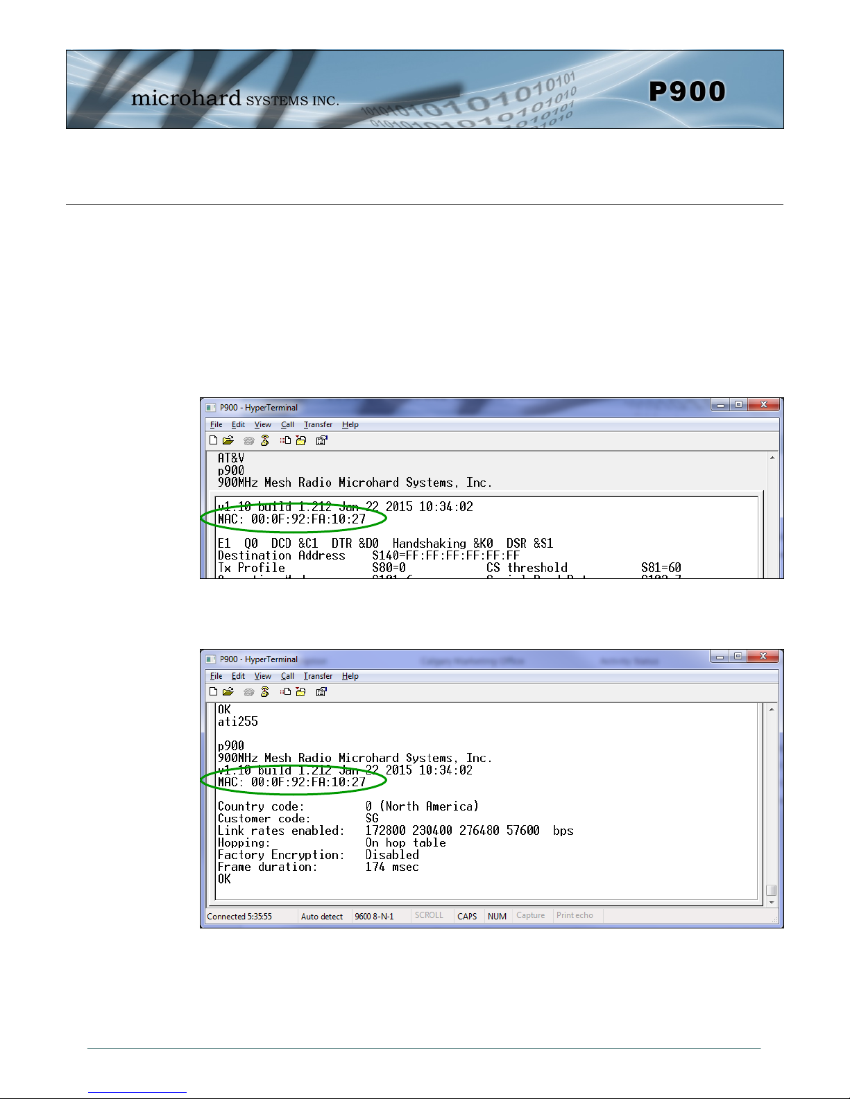
3.0 Mesh Configuration
3.2.3 Unit Addressing
Each unit is factory assigned a hardcoded MAC address that can not be changed. Using factory assigned addressing simplifies the configuration process, as addresses do not have to be manually assigned and minimizes errors that are often created when duplicate address are accidently used. In applications where the data is to be broadcasted to all units in the network, the value FF:FF:FF:FF:FF:FF is
used as a destination address in register S140. It is possible to replace the MAC address with a value in
S105. See the register S87 for more information.
For unicast operation, the specific unit address must be used. This address can be retrieved by using
the AT&V command as highlighted below.
Image 3-8: Retrieving unit MAC Address from AT&V output
It can also be viewed using the ATI commands. ATI255 will show the MAC address as well as some
additional information seen in the image below. ATI7 will show just the MAC Address.
Image 3-9: Retrieving unit MAC Address from ATI255 Output
© Microhard Systems Inc. Confidential 44
Page 45

3.0 Mesh Configuration
3.2.4 Collision Mitigation
In Mesh topology, as with most wireless systems, one of the primary challenges is the management and
mitigation of data collisions. The following section covers several complex interwoven concepts and
options that are used to provide robust, low latency communication, while minimizing the effects of data
collisions. It is important to plan and design the network layout with these concepts in mind from the
start, rather than try to cope with collisions after the system is deployed.
3.2.4.1 Channel Access Mode
To coordinate transmissions from multiple devices and to manage and minimize data collisions, the Pico
Series uses three different channel access modes. The recommended mode is purely a function of the
type of data being sent. The three modes are Aloha, RTS/CTS and TDMA, which are set using register
S244. In systems that send small bursts of data and do not want account for the overhead of CTS/RTS,
Aloha mode may be the best solution. For systems sending large packets of data with a low tolerance
for data loss or collisions, RTS/CTS may be best.
S244 = 0 - Aloha
S244 = 1 - RTS/CTS
S244 = 2 - TDMA (transmit on slot number)
Aloha
In a Mesh based system frames are used to maintain a time reference, and to keep the system synchronized. The frame is composed of a number of different attributes, one of which is a configurable number
of Aloha slots (S214). Aloha slots are used for all data communication. When the channel access mode
is set to Aloha, the transmitting modem randomly selects a Aloha slot within any frame to begin its data
transmission.
The randomness at which modems attempt to access the channel using Aloha is configurable using
register S115. The importance of this register becomes apparent when a system is such that many devices attempt to either access the channel at the same time, or transmit data often, increasing the
chances of data collisions. Increasing the randomness (S115) will make it less likely that collisions occur, but at the cost of added latency and reduced throughput. It is difficult to suggest a value for S115,
as it is impacted by the type, and frequency of data transmissions. A good starting point may be to set
the value of S115 to the (number of devices in the system) / 2, so if you have 10 total units in the network, try a value of 5 to start with.
S115 = 1 - Repeat Interval (0-255)
For systems using polling mechanisms (polled protocols, Master/Remote systems) , or if the devices
infrequently send data at staggered times, the default value of 1 is recommended, as these types of
systems have a low risk of data collisions.
If multiple modems in a system need to transmit at the same time, CSMA (Carrier Sense Multiple Access) is used to detect if the channel is currently in use. If the channel is determined to be busy, the
modem will select another random Aloha slot to begin its data transmission. Carrier Detect Threshold is
covered in more detail later in this document.
The number of aloha slots have a direct impact on the size of the frame and as a result the hop interval,
which is the amount of time spent on any one channel. Increasing the number of aloha slots will increase the number of slots available for data transmission, but at the risk of being affected by interference or noise on a channel. A short hop interval, or reduced number of aloha slots will make the system
more immune to outside interference and noise, but at the cost of reduced throughput.
© Microhard Systems Inc. Confidential 45
Page 46

3.0 Mesh Configuration
In a clean system or in areas where interference and noise are not an issue, it is ideal to allow as many
aloha slots as possible. Although the maximum configurable number of aloha slots is 255, it may not be
possible to use this number and the system will generate an error. The maximum number is determined
by considering the link rate, the number of sync slots and the number of aloha slots. FCC limits the hop
interval at a maximum of 400ms. The ATI255 command shows the current frame duration
S214 = 60 - Number of Aloha Slots (1-255)
S214 must be set to the same value on all units in the system. Failure to do so will prevent the unit from
synchronizing and being able to participate is data communication.
RTS/CTS
When register S244 = 1, the Channel Access Mode is set to RTS/CTS. In this mode, before sending
data, the modem will request a channel from the Coordinator. Once the Coordinator fulfills this request,
the modem is free to transmit its data. This type of channel access mode is best suited for systems that
require large packets of data with a low tolerance for collisions or retransmissions.
As with Aloha mode, RTS/CTS also uses S115 to provide randomness to minimize the number of units
attempting to send a RTS (Request to Send) packet to the coordinator at the same time. The larger the
value of S115 the more random the channel access becomes, reducing collisions. The cost of making
the value of S115 too large, thus increasing the randomness at which devices attempt to access the
channel, is increased latency and reduced throughput. Therefore it is important to select a value that
minimizes collisions, yet not too large to impact system performance.
TDMA
When register S244 = 2, the Channel Access Mode is set to TDMA. In this mode each modem in the
system starts its transmission on an assigned slot number within the frame. The slot number is defined
by S221.
3.2.4.2 Carrier Sense
Carrier Sense Multiple Access (CSMA) is enabled by default and is used to detect if other units are
transmitting data by measuring the signal level and determining if the level detected indicates that another unit is transmitting data. The CS Threshold can be modified using S81.
S81 = 60 - Carrier Detect Threshold in -dBm. (0-255)
The default value for S81 is –60dBm, meaning that if a modem has data to send, it will first check if
there is RF energy present and then measure the level of that energy to determine if it is noise or a valid
signal. If the detected signal is stronger than –60 dBm, if will assume that the channel is busy. If the
signal detected is weaker than the threshold, the unit will determine that the channel is free.
The Carrier Detect Threshold can be set individually on each unit in the system, as the noise floor, interference and received signal strength will vary by location. It is not recommended to adjust the value of
S80, unless the environment is well understood.
Caution: Setting a
value of S81 too low
will prevent all
communication.
© Microhard Systems Inc. Confidential 46
Page 47

3.0 Mesh Configuration
3.2.4.3 TX Profiling and Ranking
Ranking allows wide area systems with several coordinators a mechanism to segregate and control
transmissions to mitigate collisions in overlapping coverage areas. Each Coordinator in a system is
automatically assigned a rank, starting with the Primary Coordinator always being assigned Rank 0. Up
to 4 levels of ranking are used, and then are repeated for systems that require more layers. Remote
units will always associate with the lowest rank coordinator they can hear, regardless of proximity.
Ranking information is sent in each sync packet. It is possible to manually assign the coordinator rank
by using S220.
The drawing below illustrates how the ranking areas work. Notice that all devices that can hear the Primary Coordinator (Rank 0), are assigned Rank 1. In the overlapping coverage area, the units can hear
both the Primary and Secondary Coordinators, but they are also assigned rank 1, as the Primary Coordinator is the lowest ranked coordinator. The remaining units which are in the Secondary Coordinators
(Rank 1) coverage area are assigned rank 2. Notice that with the addition of Secondary Coordinators
the Rank is incremented by 1. Once reaching Rank 3, the process begins again at Rank 0. Ranking
ensures that the Mesh network maintains a stable logical structure and prevents modems from erratic
association with multiple coordinators.
Rank 3
Primary
Coordinator
Rank 2
S.C
Rank 1
Remote B
Remote A
P.C
Rank 1
S.C
S.C
Rank 2
Rank 2
Rank 2
S.C
Rank 1
Drawing 3-6: Mesh Ranking
S.C
Rank 0
Secondary
Coordinators
Rank 0
S.C
Rank 0
Rank 1
The ranking of coordinators is done automatically, and creates some structure and organization to the
Mesh Network. Tx Profiling can now use that logical separation to provide collision avoidance in the
system by assigning frames to be only used by specific ranked units, as per a TX Profile. This allows
guaranteed periods of time in which only certain ranked modems can transmit data. The result is reducing or eliminating collisions on the overlapping coverage boundaries.
© Microhard Systems Inc. Confidential 47
Page 48

3.0 Mesh Configuration
In the previous example (Drawing 3-6) we can see that Remote A and Remote B are in close proximity
of each other along an overlapping coverage boundary. Remote A can hear both the Primary and Secondary Coordinator. Even though it is closer to the Secondary Coordinator, it will associate with the Primary Coordinator as it has the lowest Rank. Remote B can only hear the Secondary Coordinator, so
obviously it can only associate with that coordinator. Without TX Profiling, there will be collision between
these units as they try to transmit. A TX profile will assign frames to each rank that they can use to send
data, without the worry that there will be collisions.
Currently there are 4 different TX Profiles. Querying the S80 register as seen below shows the TX Profile. A TX Profile is a repeating pattern of 16 frames, each frame can be assigned a rank or combination
of ranks, which are allowed to transmit data during that frame. A value of 0xF, or F in hex means that
any unit can send data, essentially meaning that TX Profiling is not used for that frame and any rank
modem can send data.
Image 3-10: TX Profiles
R3 R2 R1 R0 TX
0 0 0 1 0x1
0 0 1 0 0x2
0 1 0 0 0x4
1 0 0 0 0x8
1 1 1 1 0xF
Profile
Table 3-1: TX Profiles
Description
Rank 0 can TX
Rank 1 can TX
Rank 2 can TX
Rank 3 can TX
All Ranks can TX
As seen in the table each Hex Value in the pattern corresponds to a specific rank(s) able to transmit
during a specified frame. The TX Profile used can be set by using register S80, currently there are 4
different profiles. In future releases additional profiles may be available.
S80 = 0 - TX Profile (0-3)
Profile 0 allows any modem to send data regardless of rank, this essentially disables TX Profiling. This
is the default, as TX profiling is generally only useful in partially overlapping coverage areas where collision rates are high.
Profile 1 allows the bandwidth to be split equally between the Primary Coordinator and all rank 1 units.
This may be useful in system where there are no secondary coordinators, as there are no frames assigned to any units other than the Primary Coordinator and its’ associated units.
Profile 2 allows rank 1 units to have 1/2 of the bandwidth. The reason for this is in many systems, the
Primary Coordinator is generally located in a location that provides the greatest coverage, meaning it
generally has the most units associated with it. The rest of the bandwidth is split between the rank 2 and
rank 3 modems. The Primary Coordinator is given only 1 frame for occasional transmissions.
Profile 3 allocates most of the bandwidth to Rank 1 units with only 2 in 16 frames available for the Rank
0 coordinator. This profile is used in systems with no additional coordinators, where the units send data
a majority of the time, with the occasional transmission from the Primary.
© Microhard Systems Inc. Confidential 48
Page 49

3.0 Mesh Configuration
3.2.5 Retransmissions
Packet Retransmissions can be used to ensure data reaches its intended destination by resending the
same packet over and over unless acknowledged by the recipient. While this is an effective tool to add
system robustness, it has large impact on the performance of the system in broadcast mode. The more
times a modem retransmits data, the more the overall throughput of the system is reduced. To adjust
the retransmission rate, use register S113, the default value is 5 (+ the initial transmission).
S113 = 5 - Packet Retransmissions (0-254)
While retransmissions can provide some correction for data collisions, it is not advisable as adding retransmission may actually amplify the number of collisions. Retransmissions are typically used in noisy
environments to combat interference and low signal strength, ensuring data is received at the intended
destination.
3.2.6 Network Synchronization
Network Synchronization is what allows all units to hop from frequency to frequency at the same time.
Each Mesh Frame contains a configurable number of sync slots, that the coordinators can use to send
synchronization data. Sync data does not need to be sent during each frame, and is therefore configurable using register S216
S216 = 3 - Mesh Duty Cycle (1-100)
Register S216 defines how often the coordinator transmits sync packets (1-100). After each sync packet
transmission the coordinator picks a random number from 1 to the value in S216 and transmits the next
packet in this slot.
If the network is busy with traffic it is not necessary to send the sync packet very often, as the sync data
is also embedded into the data stream. For idle systems, an increased number of sync packets allows
for faster synchronization of new units. However, the higher the value of S216, the longer it will take for
new units to find and synchronize with a coordinator.
In large systems with many coordinators, it may be necessary to adjust the number of available sync
slots per Mesh frame to allow adequate slots for each coordinator to transmit sync data. This can be
adjusted using S215.
S215 = 1 - Number of Mesh Sync Slots (1-10)
Adding an unnecessary number of sync slots adds to the length of the Mesh Frame, which in turn creates a longer hop interval (number of sync slots + number of aloha slots = hop interval), increasing overhead and reducing system performance.
For units to synchronize with the network, each unit must have the same:
- Network ID (S104), Network Type (S133), Forward Error Correction (S158) and
- the same number of Aloha Slots (S214), number of Sync Slots (S215).
In Mesh without roaming, Hop Pattern (S106) and Hop Zone (S180) must also match.
© Microhard Systems Inc. Confidential 49
Page 50

3.0 Mesh Configuration
Sync Timeout
Once synchronized to the network the unit does not need to receive sync data often to keep track of
where the system is supposed to be (in time and frequency). The sync Timeout defines the number of
frames where no sync data is received from a coordinator before losing sync. In other words, how long a
unit will remain synchronized with the network without receiving any sync packets before it gives up and
loses sync.
S248 = 100 Sync Timeout (4-65534)
Setting a value too low will cause the unit to lose sync easily and time will be wasted trying to re-sync to
the network. As seen with the Mesh Duty Cycle several frames can go by without receiving a sync
packet, and this is completely normal. If this value is set too high, the unit will assume for a long time
that the network is still out there, when especially in mobile applications, it may not be.
Quick Sync
In a quiet Mesh network it may take some time to synchronize the entire network. To overcome this
problem, Quick Sync is used by coordinators when they first come online to quickly send a number of
sync packets on random frequencies in the current hop table. This allows the network to synchronize
much faster than waiting for the standard sync packets to arrive (which is based on the sync duty cycle
and number of sync slots). The number of sync packets sent upon power up is defined by the S151 register.
S151 = 500 Quick Sync Packets (5-65534)
When a Primary Coordinator goes online it will send the configured number of sync packets. Once a
Secondary Coordinator is synchronized, it will also transmit quick sync packets based on their configured S151 value.
No data transmission can occur while the coordinators are sending quick sync packets, even if all units
are synchronized.
When setting the S151 register, selecting a large value may create an unnecessary delay in data transmission on system startup. A value too low, or not sending enough sync packets to cover all the frequencies in the Hop Pattern will result in slower synchronization of the system as any units that did not
hear the quick sync packets will need to wait until they receive a standard sync packet to synchronize.
North America FCC requires that different 50 frequencies(channels) are used to create the hop pattern.
The default value of 500 means that 10 packets are sent on each channel to ensure system wide synchronization. Customers located in other regions or government organizations who allow or require
more or less entries in the hop pattern may decide that the default value is not appropriate for their systems, and are free to adjust this value.
© Microhard Systems Inc. Confidential 50
Page 51

3.0 Mesh Configuration
3.2.7 Routing
For Mesh Networking to be an effective networking topology, routing functions must be performed to
discover paths within the network to each destination, to ensure the best path is chosen. All units in a
Mesh Network, including remotes, can be configured to provide routing capabilities by setting register
S223.
S223 = 0 - Routing Disabled
S223 = 1 - Routing Enabled
All traffic in a Mesh system is either broadcast, where data is sent to everyone; or unicast, where data is
sent to a specific destination. Anytime there is no direct line of sight with a primary coordinator, additional coordinators can be added to extend the network. If data is transmitted to a unicast destination,
the modems will use a Microhard routing protocol to find a route by initiating route discovery. At this
point routing is required to provide route information and load balancing of the network traffic. Routing is
a key element in Mesh network design that can have a profound impact on overall system performance.
The diagram below shows a sample Mesh Network comprised of a Primary Coordinator, a Secondary
Coordinator and 11 remotes. Routing has been enabled on the Secondary Coordinator and two of the
remotes to provide comprehensive routing capabilities. It is always a good idea to assign routing operation to more than one unit to provide redundancy, and to provide alternate paths for routed data to
travel, essentially sharing the load of the network. Generally remotes sitting on the edge of the network
are not required to perform routing.
Primary
Coordinator
P.C.
Secondary
Coordinator
RT
RT
S.C
RT
Routing
Enabled
As traffic flows through and around a network, routing tables in each unit will be populated using
route discovery and routing requests as required routes are discovered. Eventually the entire network is
converged, meaning a path to all units are mapped, until something changes - a unit moves, a unit is
added, or a unit is removed from the system. When this happens, the routing table(s) must be updated.
© Microhard Systems Inc. Confidential 51
Drawing 3-7: Mesh Network w/Routing
Page 52

3.0 Mesh Configuration
Attempts before Re-Routing
Once a route is entered into the routing table, it is assumed that the route exists and can be used for
data transfer. To ensure that the information in the routing table is up to date and accurate, each time a
packet is sent to a destination the register S126 tracks the number of consecutive failed attempts to
send data before route discovery is triggered. Since all unicast data is acknowledged, the unit will know
if the packet was delivered successfully or not.
S126 = 9 - Number of Attempts before starting route discovery (1-255)
Configuration of S126 must consider multiple factors, the first is the number of retransmissions (S113)
set in the system. The value of S126 must be set higher than the total number of retransmissions.
The next consideration is the collision rate of the system. If an occasional collision is expected, this may
result in a number of unsuccessful attempts to deliver data, but it does not mean that the path is not
valid. Setting the value of S126 lower than the initial transmission + retransmissions + collisions or
packet lose due to noise or interference, may result not only in unneeded route discovery, which has a
large amount of overhead, but it could also result in a system that will never retain a route and become
completely unusable.
© Microhard Systems Inc. Confidential 52
Page 53

3.0 Mesh Configuration
Routing Request TTL
When a modem gets a packet to deliver and it does not have a route listed for that packet in the routing
table it initiates a routing request. During the routing request, and route discovery, all transmissions from
this device are stopped until the request is complete. Since several routes may be available, the modem
will wait until the entire Routing Request TTL (S219) has completed, and then pick the best path based
on a Microhard path cost calculation discussed in the next section.
S219 = 10 - Routing Request Timeout in 10ms ticks (1-10000 ticks)
The default value for S219 is 10 ticks, which means that it will wait 100ms for all possible routes to be
returned, or for the request to simply timeout if no routes are found. If the routing request times out, the
request is repeated up to 3 times automatically before the packet is discarded.
Finding the right value for S219 can be difficult. Setting a value too low may not result in the best path
being reported, or maybe not even time enough at all to receive routing information. A value too long will
affect system performance because the devices will wait unnecessary amounts of time for routing discovery to complete when they may have already received the best route.
The best option for determining an ideal value for S219, without knowing what the worst case scenario
is for the time it takes for packets to traverse a fully loaded network, would be to set the timeout to a
small value to where no data is being exchanged. Then slowly increase the value to where data is being
exchanged successfully, and then add a few more ticks.
Cost of Routes
During the routing request / route discovery process, more than one route may be returned as a possible candidate for the best route. Determining which route is the best route can be determined by calculating a cost metric using the number of hops and the signal strength between hops. The following formula allows a user to influence the relationship between the number of hops and the overall health of
the path based on RSSI.
Cost = (Number of Hops x Cost of a Hop) + (Cost of RSSI)
The number of hops and the RSSI are actual measured values in the system, automatic to the calculation. The cost of RSSI is set by the modem based on the measured value between hops. The stronger a
signal, the lower its cost as seen in the relationship below.
Very High
© Microhard Systems Inc. Confidential 53
Cost
None
0 -20 -40 -60 -80 -100 =110…..
RSSI
Drawing 3-8: Cost of RSSI vs RSSI
Page 54

3.0 Mesh Configuration
Actual cost of RSSI used by Microhard to determine route cost is listed in the table below:
The cost of a hop can be modified by the user by setting register S245. Setting this register influences
the relationship between the number of hops and the signal strength of the path.
S245 = 100 - Cost of one hop in Mesh (0-255)
Setting the value of S245 low, in relation to the cost of RSSI would result in a path that is not concerned
with the number of hops, so long as the signal between hops was strong. Setting the value of S245 to a
high cost value would indicate that using the shortest path possible is the most important, resulting in
low latency and increased throughput, even at the risk of the path being weak, resulting in lost packets
and retransmissions.
The illustration shows how different paths are calculated, and how the best path is determined before
being added to the routing table.
Cost of RSSI RSSI (dBm) Cost of RSSI RSSI (dBm) Cost of RSSI RSSI (dBm)
0 Less than 55 10 79 26 92
1 55 - 59 11 80 28 93
2 60 - 64 12 81 32 94
3 65 - 67 13 82 35 95
4 68 - 69 14 83 38 96
5 70 - 71 16 84 40 97
6 72 - 73 18 85 44 98
7 74 - 75 19 86 49 99
8 76 - 77 20 87 50 100
9 78 21 88 - 91 50 100+
Table 3-2: Cost of RSSI
A
-67dBm
(3)*
Path 1
*Cost of RSSI
© Microhard Systems Inc. Confidential 54
R1
-54dBm
(0)*
Path 2
-91Bm
(21)*
Path 3
R2
-72dBm
(6)*
-97dBm
(40)*
R3
-52dBm
(0)*
B
Drawing 3-8: Routing Path Cost
Shows the path cost from Modem A to Modem B.
Path Path Cost (Cost of hop =100) # Hops
1 (2x100) + 3 + 21 = 224 2
2 (2x100) + 0 +40 = 240 2
3 (3x100) + 0 + 6 + 0 = 306 3
Path Path Cost (Cost of hop =10) # Hops
1 (2x10) + 3 + 21 = 44 2
2 (2x10) + 0 +40 = 60 2
3 (3x10) + 0 + 6 + 0 = 36 3
Page 55

3.0 Mesh Configuration
As seen in the first table of the illustration, using a cost of hop of 100, results in Path 1, which is the
shortest path, being the lowest cost and the preferred route. It has the least amount of hops and even
though the signal strength between hops may not be ideal, it is considered the preferred route and
added to the routing table.
The second table of the illustration shows the effect of changing S245 to a small value, S245 = 10, lowering the cost of each hop. The results for this scenario have much different result. Since the cost of
each hop is very low, and the strength of the links between hops is very strong, Path 3 results in being
the lowest.
As seen, changing the value of S245 can drastically change the results. It should also be noted that the
S245 can be modified on each unit, again changing the “best” path as seen by the route discovery proc-
ess.
3.2.8 Hop Pattern
Frequency Hopping modems hop from frequency to frequency to allow for multiple networks to share
the same frequency spectrum. The pattern at which the modems hop is known as the hopping pattern.
In the Pico Series modems the hop pattern is pseudo-randomly generated using a complex combination
of the Network ID (S104), Register S106, and S180, which define which channels are to be included in
the calculation. This ensures that no two networks have the same hopping pattern, which would cause
interference and collisions.
Register S106: Hop Pattern selects the hop pattern to use for the current system. The value set in this
register must be the same for each unit in the system
S106 = 0 - Selects Hopping Pattern
FCC requires that FHSS systems hop on 50 different channels within the 900 MHz ISM Band. The
maximum time spent on any one channel must not exceed 400ms.
To calculate the center frequency represented by each channel only the starting frequency and the size
of each channel (Channel Bandwidth) need to be known. For the 900 MHz ISM Band, the starting frequency is 902.4 MHz, and the Channel Bandwidth is dependent on the current link rate.
Freq channel n = 902.4+ ((n-1) x BW)MHz.
Example: Channel 75 @ 172 kbps = 902.4 +((75-1) x 0.250) MHz
902.4 + (74 x 0.250) MHz
902.4 + 18.5 MHz
920.9 MHz
Link Rate
(bps)
57600 100
115200 200
172800 250
230400 280
276480 350
Channel
Bandwidth
(kHz)
© Microhard Systems Inc. Confidential 55
Page 56

3.0 Mesh Configuration
Hop Zones
Register S180: Hop Zone selects the available frequency zones used by the Pico Series, as there may
be times when multiple systems are deployed within close proximity, or there may be outside interference or noise that requires sections of the available spectrum to not be included in the Hop Pattern generation.
S180 = 0 - Use Entire 902-928 MHz ISM Band
Several Hop Zones are predefined by querying the S180 Register as seen below. The ranges listed are
the frequency ranges that are available to create the hop table. Using Hop Zones several frequency
Bands can be excluded. Also if multiple systems are being deployed within close proximity, Hop Zones
can be used to minimize overlap in the frequencies used to populate the Hopping Pattern.
© Microhard Systems Inc. Confidential 56
Image 3-11: Hop Zones
Page 57
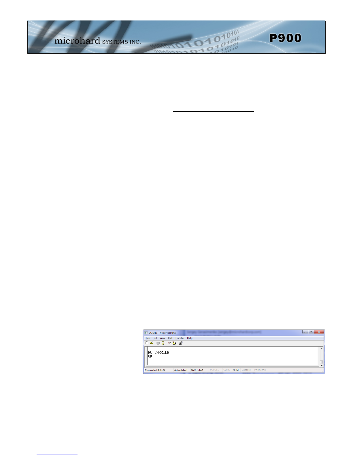
4.0 Point to Point Configuration
To begin configuration, the P900 must be mounted into a either a Microhard supplied development
board (with factory attached interface card), or be mounted into a customer designed platform. The
P900 is configured using AT commands through the Data port, or using special diagnostic commands
through the Diagnostic Port. Refer to Section 2: Hardware Description for information related to inter-
facing to, or powering the module.
To issue AT commands through the Data port, the P900 must first be set into Command Mode as described below.
4.1 Configuration/Unit Modes
4.1.1 Command Mode
the P900 module is offline (data is not passing through the unit via it’s local data lines
or RF communications)
if installed in a Development Board, the only LED illuminated will be the blue power
LED.
the P900’s configuration options (registers) may be viewed and modified using AT
commands.
Two methods are typically used to place the Pico Series into Command Mode.
1. Force to Command Mode
Power down off the Development Board assembly.
Connect a 9-pin straight-through serial cable from the PC serial port to the rear RS-
232 port (DATA) of the modem.
Launch a terminal communications program (e.g. HyperTerminal) and configure for
9600bps, 8 data bits, No parity, 1 stop bit (8N1), no flow control
press and hold the CONFIG button
continue to press the CONFIG button and apply power to the modem
release the CONFIG button
On power up the terminal session window should show “NO CARRIER OK” as seen
below:
the P900 is now in command mode, and AT commands can be used to configure or
query the settings. AT&V will display the current configuration, and the registers can
be queried using the ATSXXX=? Command where XXX = the register number. Help is
available using the ATSXXX /? Command.
Any and all changes must be written to NVRAM using the AT&W command.
Image 4-1: Command Mode
© Microhard Systems Inc. Confidential 57
Page 58

4.0 Point to Point Configuration
2. Escape from Data Mode
With the P900 powered up and ‘online’, connect a 9-pin straight-through serial cable
from the PC serial port to the RS-232 DATA port on the dev board.
Launch a terminal program (e.g. HyperTerminal) and configure for the P900’s estab-
lished serial baud rate parameters (PC & modem must match).
Pause 1 second, type ‘+++’ , pause 1 second: the monitor should show the module
response of ‘NO CARRIER OK’
The P900 is now in command mode, and AT commands can be used to configure or
query the settings.
Entering the AT&V command as shown will show the current configuration as seen
below: (The data displayed varies based on network and unit type.)
4.1.2 Data Mode
Data Mode is the normal operational state of all deployed P900 modules. In this mode the
module is prepared to exchange data as per its configuration settings. Available LED indications can provide an indication of the data exchange (TX and RX LEDs).
To enter DATA mode from COMMAND mode, enter the command: ATA [Enter]
Image 4-2: Command Mode
Image 4-3: Command Mode - AT&V Display
© Microhard Systems Inc. Confidential 58
Page 59

4.0 Point to Point Configuration
4.2 Point to Point Network
In a point-to-point network, a path is created to transfer data between Point A and Point B, where Point
A may be considered the Master modem and Point B a Slave. Such a PTP network may also involve
one or more Repeaters (in a store-and-forward capacity) should the radio signal path dictate such a
requirement. Point to Point is enabled by setting register S133 to 1 (ATS133=1, Network Type).
A PTP configuration may also be used in a more dynamic sense: there may be many Slaves (and Re-
peaters) within such a network, however the Master may have its ‘Destination Address’ (S140) changed
when required to communicate with a specific Slave.
Master
Master
Drawing 4-1: Point to Point Network Topology
OR
Repeater
Slave
Slave
4.2.1 Operating Modes / Unit Types
In a Microhard Point to Point Network, three unit types or operating modes are available: the Master,
Repeater, and the Remote. The Masters role is to provide network synchronization for the system,
which ensures all units are active and able to communicate as required. The Master controls the flow of
data through the system; all data passes through it. The diagram below shows a unit configured as a
Master.
Master
Coverage
Area
Master
Drawing 4-2: Point to Point Master
Slave
© Microhard Systems Inc. Confidential 59
Page 60

4.0 Point to Point Configuration
Repeaters can be used to extend the coverage of the Master. Required only if it is necessary to establish a radio path between a Master and Slave(s); stores and forwards data sent to it. Synchronizes to
Master and provides synchronization to ‘downstream’ units. If a local device is attached to a Repeater’s
serial data port, the Repeater will also behave as a Slave (aka Repeater/Slave).
Adding one or more Repeaters within a network will cut the overall throughput of the network in half; the
throughput is halved only once, i.e. it does not decrease with the addition of more Repeaters. If there is
a ‘path’ requirement to provide Repeater functionality, but throughput is critical, a work around is to
place two modems at the Repeater site in a ‘back-to-back’ configuration. One modem would be configured as a Slave in the ‘upstream’ network; the other a Master (or Slave) in the ‘downstream’ network.
Local connection between the modems would be a ‘null modem’ cable. Each modem would require its
own antenna; careful consideration should be given with respect to antenna placement and modem
configuration.
Master
Repeater
Repeater
Drawing 4-3: Point to Point Repeater
Slave
A Slave (Remote) is an endpoint/node within a network to which a local device is attached. Communi-
cates with Master either directly or through one or more Repeaters.
Slave
Master
Repeater
Slave
Drawing 4-4: Point to Point Slave
Units can be configured to perform the various roles discussed by setting register S101 as follows:
ATS101 = 0 - Master
ATS101 = 1 - Repeater
ATS101 = 2 - Slave (Remote)
© Microhard Systems Inc. Confidential 60
Page 61

4.0 Point to Point Configuration
4.2.2 Configuration Using Factory Defaults
Factory default setting commands can be used to aid in the configuration and deployment of the Pico
series modules, providing a known starting point in the configuration process for each unit type. Using
the factory default commands sets all applicable registers to factory recommended settings and allows
for initial connectivity between units. Configuring modems using the factor default settings have the following benefits:
hastens the configuration process - load default settings and, if necessary, apply only minor
For many networks, the factory default commands may be all that is necessary to configure and deploy
a simple Point to Point Network. Other applications may require additional registers to be configured.
Regardless of the complexity of the configuration, the factory default settings provide a starting point for
all configurations. All unit types have have a factory default setting command.
AT&F10 - Point to Point Master
AT&F11 - Point to Point Slave
AT&F12 - Point to Point Repeater
The screen shots for each unit type highlight the key registers that are automatically changed to create
a Point to Point configuration. There may also be additional registers such as the Network ID that are
recommended to be changed.
settings / adjustments
aids in troubleshooting - if settings have been adjusted and basic communications cannot be
established, simply revert to the factory default setting and any improper adjustments will be
overwritten and a ‘fresh start’ can be made with known-to-work settings
Each PTP Network
must have a unique
network ID. This can
be changed using
register S104: Network
Address.
© Microhard Systems Inc. Confidential 61
Image 4-4: Factory Defaults
Page 62

4.0 Point to Point Configuration
AT&F10 Point to Point Master
A
B
C
D
E
F
G
I
J
Compression (S225)
was introduced in
firmware v1.10. S225
must be set to 0 for
compatibility with older
versions.
H
K
Image 4-5: Factory Defaults AT&F10 - Point to Point Master
A) AT&F10 - Sets the factory defaults for a Point to Point Master.
B) AT&W - Writes the changes to NVRAM.
C) AT&V - Displays the configuration as seen above.
D) S105 - Every unit in a Point to Point Network must have a unique unit address. The Master is
automatically set to 1, and should not be changed.
E) S140 - The destination address is unit address of the final destination, which all data is to
be sent. The address entered would generally be the unit address of the Slave.
F) S101 - The operating mode defines the unit type and is set to 0, which is a Master.
G) S103 - Wireless Link Rate must be set to the same value of each unit in the system.
Higher link rates may result in higher throughput, but lower link rates usually
provide better sensitivity and overall robustness.
H) S133 - The network type must be set to 1 for Point to Point operation. The content displayed
by the AT&V command will vary with the network type.
I) S102 - The serial baud rate (and data format S110) must match that of the connected device.
J) S104 - Each unit in a Network must have the same Network Address. It is strongly
recommended to never use the default setting of 1234567890. To change the
Network Address, the ATS104=XXXXXXX command can be used.
K) S141 - This register informs the master if 1 or more repeaters are present in the system. This
applies only to the master radio.
Remember, anytime registers are changed the values must be written to NVRAM using the AT&W command. To switch from command mode to data mode (online mode), the ATA command can be issued.
© Microhard Systems Inc. Confidential 62
Page 63

4.0 Point to Point Configuration
AT&F11 Point to Point Slave
A
B
C
D
E
K
H
Image 4-6: Factory Defaults AT&F11 - Point to Point Slave
F
G
L
I
J
A) AT&F11 - Sets the factory defaults for a Point to Point Slave.
B) AT&W - Writes the changes to NVRAM.
C) AT&V - Displays the configuration as seen above.
D) S105 - Every unit in a Point to Point Network must have a unique unit address. The address
of the slave (remote) is automatically set to 2. This can be changed, but ensure that
the destination address on the master is also changed!
E) S140 - The destination address is unit address of the final destination to which all data is to
be sent. In a Point to Point Network this address is set to 1, the unit address of the
master, and should not be changed.
F) S101 - The operating mode defines the unit type and is set to 2, which is a Slave (Remote).
G) S103 - Wireless Link Rate must be set to the same value of each unit in the system.
H) S133 - The network type must be set to 1 for Point to Point operation. The content displayed
by the AT&V command varies with the network type.
I) S102 - The serial baud rate (and data format S110) must match that of the connected device.
J) S104 - Each unit in a Network must have the same Network Address. To change the
Network Address, the ATS104=XXXXXXX command can be used.
K) S106 - Ensure this register is set to the Hopping Pattern of the Master(S106), or if the unit is
to communicate through a repeater, set to match the Secondary Hop Pattern (S206).
L) S118 - If the slave is to connect through a repeater, enter the unit address of the repeater
here, or set to 65535 for roaming.
© Microhard Systems Inc. Confidential 63
Page 64

4.0 Point to Point Configuration
AT&F12 Point to Point Repeater
A
B
C
D
E
K
M
Image 4-7: AT&F12 Point to Point Repeater Configuration
F
G
I
J
L
H
A) AT&F12 - Sets the factory defaults for a Point to Point Repeater.
B) AT&W - Writes the changes to NVRAM.
C) AT&V - Displays the configuration as seen above.
D) S105 - Every unit in a Point to Point Network must have a unique unit address. The address
of the Repeater is automatically set to 3.
E) S140 - The destination address is unit address of the final destination to which all data is to
be sent. In a Point to Point Network this address is set to 1, the unit address of the
master, and should not be changed.
F) S101 - The operating mode defines the unit type and is set to 1, which is a Repeater.
G) S103 - Wireless Link Rate must be set to the same value of each unit in the system.
H) S133 - The network type must be set to 1 for Point to Point operation. The content displayed
by the AT&V command varies with the network type.
I) S102 - The serial baud rate (and data format S110) must match that of the connected device.
J) S104 - Each unit in a Network must have the same Network Address. To change the
Network Address, the ATS104=XXXXXXX command can be used.
K) S106 - Ensure this register is set to the Hopping Pattern of the Master(S106), or if the unit is
to communicate through a repeater, set to match the Secondary Hop Pattern (S206).
L) S206 - This is the secondary hop pattern which is used to communicate with downstream
units.
M) S118 - The roaming address must be set to the master or repeaters’ address (if more than 1
repeater is used) in which this repeater is to synchronize with.
© Microhard Systems Inc. Confidential 64
Page 65

4.0 Point to Point Configuration
4.2.3 Retransmissions
Packet Retransmissions can be used to ensure data reaches its intended destination by resending the
same packet over and over. In Point to Point system all data is acknowledged by the destination, resulting in retransmissions only being used if no acknowledgement is received. The overall impact on system
performance, while not as significant as it is in Mesh and Point to Multipoint networks, should still be
considered. The more times a modem retransmits data, the more the overall throughput of the system is
reduced. To adjust the retransmission rate, use register S113, the default value is 5 (+ the initial transmission).
S113 = 5 - Packet Retransmissions (0-254)
Retransmissions are typically used in noisy environments to combat interference and low signal
strength, ensuring data is received at the intended destination.
4.2.4 Network Synchronization
Network Synchronization is what allows all units to hop from frequency to frequency at the same time.
For units to synchronize with the network, each unit must have the same:
- Network ID (S104)
- Forward Error Correction (S158)
- Network Type (S133)
Sync Timeout
Once synchronized to the network the unit does not need to receive sync data often to keep track of
where the system is supposed to be (in time and frequency). The sync Timeout defines the number of
hops where no sync data is received from a Master and/or Repeater before losing sync. In other words,
how long a unit will remain synchronized with the network without receiving any sync packets before it
gives up and loses sync.
S248 = 512 Sync Timeout (4-65534)
Setting a value too low will cause the unit to lose sync easily and time will be wasted trying to re-sync to
the network. Several hops can go by without receiving a sync packet, and this is completely normal. If
this value is set too high, the unit will assume for a long time that the network is still out there, when
especially in mobile applications, it may not be.
© Microhard Systems Inc. Confidential 65
Page 66

4.0 Point to Point Configuration
4.2.5 Hop Patterns
Frequency Hopping modems hop from frequency to frequency to allow for multiple networks to share
the same frequency spectrum. The pattern at which the modems hop is known as the hopping pattern.
In the Pico Series modems the hop pattern is pseudo-randomly generated using a complex combination
of the Network ID (S104), Register S106 (or S206), and S180 (or S181), which define which channels
are to be included in the calculation. This ensures that no two networks have the same hopping pattern,
which would cause interference and collisions.
Register S106: The primary Hop Pattern selects the hop pattern to use between a Master or Repeater
to communicate with its associated units. The value set in this register should be the same for each unit
that is to communicate with the specific Master or Repeater. A slave will automatically discover the hop
patterns of its Master/Repeater based on its S118 setting. Setting S106 to match its Master/Repeater
may shorten the discovery process.
Not every hop pattern is
generated orthogonally
to others, use AT&H26
command for more
information.
S106 = 0 - Primary Hopping Pattern
Register S206: The Secondary Hop Pattern selects a orthogonal, or different, hop pattern with nonoverlapping channels used by repeaters to communication with its’ associated units.
S206 = 1 - Secondary Hopping Pattern
The following illustration should help to describe how to provision the hop patterns in systems with repeaters.
Primary Hop
Pattern
Master
S106 =0 S106 = 0
Repeater
S206 = 1
Drawing 4-5: Hop Pattern (PP)
Secondary
Hop Pattern
Slave
Repeater
S106 = 1
S206 = 2
Primary Hop
Pattern
Slave
S106 =2
FCC requires that FHSS systems hop on 50 different channels within the 900 MHz ISM Band. The
maximum time spent on any one channel must not exceed 400ms.
To calculate the center frequency represented by each channel only the starting frequency and the size
of each channel (Channel Bandwidth) need to be known. For the 900 MHz ISM
Band, the starting frequency is 902.4 MHz, and the Channel Bandwidth is dependent on the current link
rate.
Freq channel n = 902.4+ ((n-1) x BW) MHz.
Example: Channel 75 @ 172 kbps = 902.4 +((75-1) x 0.250) MHz
902.4 + (74 x 0.250) MHz
902.4 + 18.5 MHz
920.9 MHz
Link Rate
(bps)
57600 100
115200 200
172800 250
230400 280
276480 350
Channel
Bandwidth
(kHz)
© Microhard Systems Inc. Confidential 66
Page 67
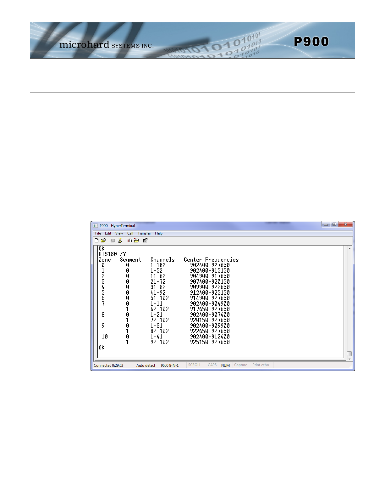
4.0 Point to Point Configuration
Hop Zones
Register S180: Hop Zone and S181: Secondary Zone, select the available frequency zones used by
the Pico Series, as there may be times when multiple systems are deployed within close proximity, or
there may be outside interference or noise that requires sections of the available spectrum to not be
included in the Hop Pattern generation.
S180 = 0 - Primary Zone (0=Use Entire 902-928 MHz ISM Band)
S181 = 0 - Secondary Zone
The Primary Hop Zone, S180 is applied to the Primary Hop Pattern (S106). The Secondary Hop Zone,
is applied to the Secondary Hop Pattern (S206), when determining the hop pattern for each segment of
the system.
Several Hop Zones are predefined by querying the S180 Register as seen below. The ranges listed are
the frequency ranges that are available to create the hop table. Using Hop Zones several frequency
Bands can be excluded. Also if multiple systems are being deployed within close proximity, Hop Zones
can be used to minimize overlap in the frequencies used to populate the Hopping Pattern.
© Microhard Systems Inc. Confidential 67
Image 4-8: Hop Zones
Page 68

5.0 Point to Multipoint Configuration
To begin configuration, the P900 must be mounted into a either a Microhard supplied development
board (with factory attached interface card), or be mounted into a customer designed platform. The
P900 is configured using AT commands through the Data port, or using special diagnostic commands
through the Diagnostic Port. Refer to Section 2: Hardware Description for information related to inter-
facing to, or powering the module.
To issue AT commands through the Data port, the P900 must first be set into Command Mode as described below.
5.1 Configuration/Unit Modes
5.1.1 Command Mode
the P900 module is offline (data is not passing through the unit via it’s local data lines
or RF communications)
if installed in a Development Board, the only LED illuminated will be the blue power
LED.
the P900’s configuration options (registers) may be viewed and modified using AT
commands.
Two methods are typically used to place the Pico Series into Command Mode.
1. Force to Command Mode
Power down off the Development Board assembly.
Connect a 9-pin straight-through serial cable from the PC serial port to the rear RS-
232 port (DATA) of the modem.
Launch a terminal communications program (e.g. HyperTerminal) and configure for
9600bps, 8 data bits, No parity, 1 stop bit (8N1), no flow control
press and hold the CONFIG button
continue to press the CONFIG button and apply power to the modem
release the CONFIG button
On power up the terminal session window should show “NO CARRIER OK” as seen
below:
the P900 is now in command mode, and AT commands can be used to configure or
query the settings. AT&V will display the current configuration, and the registers can
be queried using the ATSXXX=? Command where XXX = the register number. Help is
available using the ATSXXX /? Command.
Any and all changes must be written to NVRAM using the AT&W command.
Image 5-1: Command Mode
© Microhard Systems Inc. Confidential 68
Page 69

5.0 Point to Multipoint Configuration
2. Escape from Data Mode
With the P900 powered up and ‘online’, connect a 9-pin straight-through serial cable
from the PC serial port to the RS-232 DATA port on the dev board.
Launch a terminal program (e.g. HyperTerminal) and configure for the P900’s estab-
lished serial baud rate parameters (PC & modem must match).
Pause 1 second, type ‘+++’ , pause 1 second: the monitor should show the module
response of ‘NO CARRIER OK’
The P900 is now in command mode, and AT commands can be used to configure or
query the settings.
Entering the AT&V command as shown will show the current configuration as seen
below: (The data displayed varies based on network and unit type.)
4.1.2 Data Mode
Data Mode is the normal operational state of all deployed P900 modules. In this mode the
module is prepared to exchange data as per its configuration settings. Available LED indications can provide an indication of the data exchange (TX and RX LEDs).
To enter DATA mode from COMMAND mode, enter the command: ATA [Enter]
Image 5-3: Command Mode - AT&V Display
Image 5-2: Command Mode
© Microhard Systems Inc. Confidential 69
Page 70

5.0 Point to Multipoint Configuration
5.2 Point to Multipoint Network
In a Point to Multipoint Network, a path is created to transfer data between the Master modem and numerous remote modems. The remote modems may simply be Slaves with which the Master communicates directly, and/or Slaves which communicate via Repeaters. Some or all of the Repeaters may also
act as Slaves in this type of Network, i.e. the Repeaters are not only storing and forwarding data, but are
also acting as Slaves. Such Repeaters may be referred to as ‘Repeater/Slaves’. Point to Multipoint is
enabled by setting register S133 to 0 (ATS133=0, Network Type).
Slave
Master
Slave
Repeater
Slave Slave
Drawing 5-1: Point to Multipoint Network Topology
5.2.1 Operating Modes / Unit Types
In a Microhard Point to Multipoint Network, three unit types or operating modes are available: the Master, the Repeater, and the Remote. The Master modem’s role is to provide network synchronization for
the system, which ensures all units are active and able to communicate as required. The Master controls the flow of data through the system; all data passes through it. The diagram below shows a unit
configured as a Master.
Master
Slave
Coverage
Area
Master
Slave
Drawing 5-2: Point to Multipoint Master
Slave
© Microhard Systems Inc. Confidential 70
Page 71

5.0 Point to Multipoint Configuration
Repeaters can be used to extend the coverage of the Master. Required only if necessary to establish a
radio path between a Master and Slave(s); stores and forwards data sent to it. Synchronizes to Master
and provides synchronization to ‘downstream’ units. If a local device is attached to a Repeater’s serial
data port, the Repeater will also behave as a Slave (aka Repeater/Slave).
Adding one or more Repeaters within a network will cut the overall throughput of the network in half; the
throughput is halved only once, i.e. it does not decrease with the addition of more Repeaters. If there is
a ‘path’ requirement to provide Repeater functionality, but throughput is critical, a work around is to
place two modems at the Repeater site in a ‘back-to-back’ configuration. One modem would be configured as a Slave in the ‘upstream’ network; the other a Master (or Slave) in the ‘downstream’ network.
Local connection between the modems would be a ‘null modem’ cable. Each modem would require its
own antenna; careful consideration should be given with respect to antenna placement and modem
configuration.
Repeater
Master
Slave Slave
Slave
Repeater
Slave
Master
Coverage
Area
Repeaters
Coverage
Area
© Microhard Systems Inc. Confidential 71
Drawing 5-3: Point to Multipoint Repeater
Page 72

5.0 Point to Multipoint Configuration
A Slave (Remote) is a endpoint or node within a network to which a local serial device is attached.
Communicates with Master either directly or through one or more Repeaters.
Master
Repeater
Slave Slave
Drawing 5-4: Point to Multipoint Slave
Slave
Slave
Slave
Repeater
Slave
Units can be configured to perform the various roles discussed by setting register S101 as follows:
ATS101 = 0 - Master
ATS101 = 1 - Repeater
ATS101 = 2 - Slave (Remote)
The next section discussed using Factory Default commands to configure the various types of units that
are available in a Point to Multipoint network, simplifying the configuration process.
© Microhard Systems Inc. Confidential 72
Page 73

5.0 Point to Multipoint Configuration
5.2.2 Configuration Using Factory Defaults
Factory default setting commands can be used to aid in the configuration and deployment of the Pico
series modules, providing a known starting point in the configuration process for each unit type. Using
the factory default commands sets all applicable registers to factory recommended settings and allows
initial connectivity between units. Configuring modems using the factor default settings have the following benefits:
hastens the configuration process - load default settings and, if necessary, apply only minor
For many networks, the factory default commands may be all that is necessary to configure and deploy
a simple Point to Multipoint Network. Other applications may require additional registers to be configured. Regardless of the complexity of the configuration, the factory default settings provide a starting
point for all configurations. All unit types have a factory default setting command.
AT&F7 - Point to Multipoint Master
AT&F8 - Point to Multipoint Slave
AT&F9 - Point to Multipoint Repeater
The screen shots for each unit type will highlight the key registers that are automatically changed to
create a Point to Point configuration. There may also be additional registers such as the Network ID that
are recommended to be changed.
settings / adjustments
aids in troubleshooting - if settings have been adjusted and basic communications cannot be
established, simply revert to the applicable factory default setting and any improper adjust-
ments will be overwritten and a ‘fresh start’ can be made with known-to-work settings
Each PMP Network
must have a unique
network ID. This can
be changed using
register S104: Network
Address.
© Microhard Systems Inc. Confidential 73
Image 5-4: Factory Defaults
Page 74

5.0 Point to Multipoint Configuration
AT&F7 Point to Multipoint Master
A
B
C
Compression (S225)
was introduced in
firmware v1.10. S225
must be set to 0 for
compatibility with older
versions.
D
E
Image 5-5: Factory Defaults AT&F7 - Point to Multipoint Master
F
G
K
I
J
H
A) AT&F7 - Sets the factory defaults for a Point to Multipoint Master.
B) AT&W - Writes the changes to NVRAM.
C) AT&V - Displays the configuration as seen above.
D) S105 - Every unit in a Point to Multipoint Network must have a unique unit address. The Mas-
ter is automatically set to 1, and should not be changed.
E) S140 - The destination address for a PMP Network, by default is 65535, which means data is
broadcast from the Master to all other units.
F) S101 - The operating mode defines the unit type and is set to 0, which is a Master.
G) S103 - Wireless Link Rate must be set to the same value of each unit in the system.
Higher link rates may result in higher throughput, but lower link rates usually
provide better sensitivity and overall robustness.
H) S133 - The network type must be set to 0 for Point to Multipoint operation. The content dis-
played by the AT&V command will vary with the network type.
I) S102 - The serial baud rate (and data format S110) must match that of the connected device.
J) S104 - Each unit in a Network must have the same Network Address. It is strongly
recommended to never use the default setting of 1234567890. To change the
Network Address, the ATS104=XXXXXXX command can be used.
K) S141 - This register informs the master if 1 or more repeaters are present in the system. This
applies only to the master radio.
Remember, anytime registers are changed the values must be written to NVRAM using the AT&W command. To switch from command mode to data mode (online mode), the ATA command can be issued.
© Microhard Systems Inc. Confidential 74
Page 75

5.0 Point to Multipoint Configuration
AT&F8 Point to Multipoint Slave
A
B
C
D
E
K
H
Image 5-6: Factory Defaults AT&F8 - Point to Multipoint Slave
F
G
L
I
J
A) AT&F8 - Sets the factory defaults for a Point to Multipoint Slave.
B) AT&W - Writes the changes to NVRAM.
C) AT&V - Displays the configuration as seen above.
D) S105 - Every unit in a Point to Multipoint Network must have a unique unit address. The ad
dress of the slave (remote) is automatically set to 2. If adding more than 1 Slave, this
will need to be modified for each unit added.
E) S140 - The destination address is the final destination to which all data is to be sent. In a
Point to Multipoint Network this address is set to 1, the unit address of the Master,
and should not be changed.
F) S101 - The operating mode defines the unit type and is set to 2, which is a Slave (Remote).
G) S103 - Wireless Link Rate must be set to the same value of each unit in the system.
H) S133 - The network type must be set to 0 for Point to Multipoint operation.
I) S102 - The serial baud rate (and data format S110) must match that of the connected device.
J) S104 - Each unit in a Network must have the same Network Address. To change the
Network Address, the ATS104=XXXXXXX command can be used.
K) S106 - Normally this register is set to the Hopping Pattern of the Master(S106), or if the unit
is to communicate through a repeater, set to match the Secondary Hop Pattern
(S206).
L) S118 - If the slave is to connect through a repeater, enter the unit address of the repeater
here. Or set to 65535 for roaming.
© Microhard Systems Inc. Confidential 75
Page 76

5.0 Point to Multipoint Configuration
AT&F9 Point to Multipoint Repeater
A
B
C
D
E
K
F
G
Image 5-7: AT&F9 Point to Multipoint Repeater
I
J
L
H
A) AT&F9 - Sets the factory defaults for a Point to Multipoint Repeater.
B) AT&W - Writes the changes to NVRAM.
C) AT&V - Displays the configuration as seen above.
D) S105 - Every unit in a Point to Multipoint Network must have a unique unit address. The ad-
dress of the Repeater is automatically set to 3.
E) S140 - The destination address is the final destination to which all data is to be sent. In a
Point to Multipoint Network this address is set to 1, the unit address of the Master,
and should not be changed.
F) S101 - The operating mode defines the unit type and is set to 1, which is a Repeater.
G) S103 - Wireless Link Rate must be set to the same value of each unit in the system.
H) S133 - The network type must be set to 0 for Point to Multipoint operation.
I) S102 - The serial baud rate (and data format S110) must match that of the connected device.
J) S104 - Each unit in a Network must have the same Network Address. To change the
Network Address, the ATS104=XXXXXXX command can be used.
K) S106 - Should normally be set to the Hopping Pattern of the Master(S106), or if the unit is
to communicate through a another repeater, set to match the Secondary Hop Pattern
(S206) of that device.
L) S206 - This is the secondary hop pattern which is used to communicate with downstream
units.
© Microhard Systems Inc. Confidential 76
Page 77

5.0 Point to Multipoint Configuration
5.2.3 Unit Addressing
In a Point to Multipoint Network each unit must have a unique unit address, which can be configured
using register S105. Duplicate addresses may result in unpredictable problems in the network. In a PMP
Network data flow is such that data from the Master is sent to all units by setting the destination address
(S140) to 65535, meaning data is broadcast to all units.
5.2.4 Retransmissions
Packet Retransmissions can be used to ensure data reaches its intended destination by resending the
same packet over and over. In Point to Multipoint system data from the master is not acknowledged by
the destination, meaning data will be transmitted an additional number of times specified by S113, resulting in a significant impact on system performance. The more times a modem retransmits data, the
more the overall throughput of the system is reduced. To adjust the retransmission rate, use register
S113, the default value is 5 (+ the initial transmission). Although, this number should be as low as possible to keep as much bandwidth in the system as possible.
S113 = 5 - Packet Retransmissions (0-254)
Retransmissions are typically used in noisy environments to combat interference and low signal
strength, ensuring data is received at the intended destination.
5.2.5 Network Synchronization
Network Synchronization is what allows all units to hop from frequency to frequency at the same time.
For units to synchronize with the network, each unit must have the same:
- Network ID (S104)
- Network Type (S133)
- Forward Error Correction (S158)
Sync Timeout
Once synchronized to the network the unit does not need to receive sync data often to keep track of
where the system is supposed to be (in time and frequency). The sync Timeout defines the number of
hops where no sync data is received from a Master and/or Repeater before losing sync. In other words,
how long a unit will remain synchronized with the network without receiving any sync packets before it
gives up and loses sync.
S248 = 512 Sync Timeout (4-65534)
Setting a value too low will cause the unit to lose sync easily and time will be wasted trying to re-sync to
the network. Several hops can go by without receiving a sync packet, and this is completely normal. If
this value is set too high, the unit will assume for a long time that the network is still out there, when
especially in mobile applications it may not be.
© Microhard Systems Inc. Confidential 77
Page 78
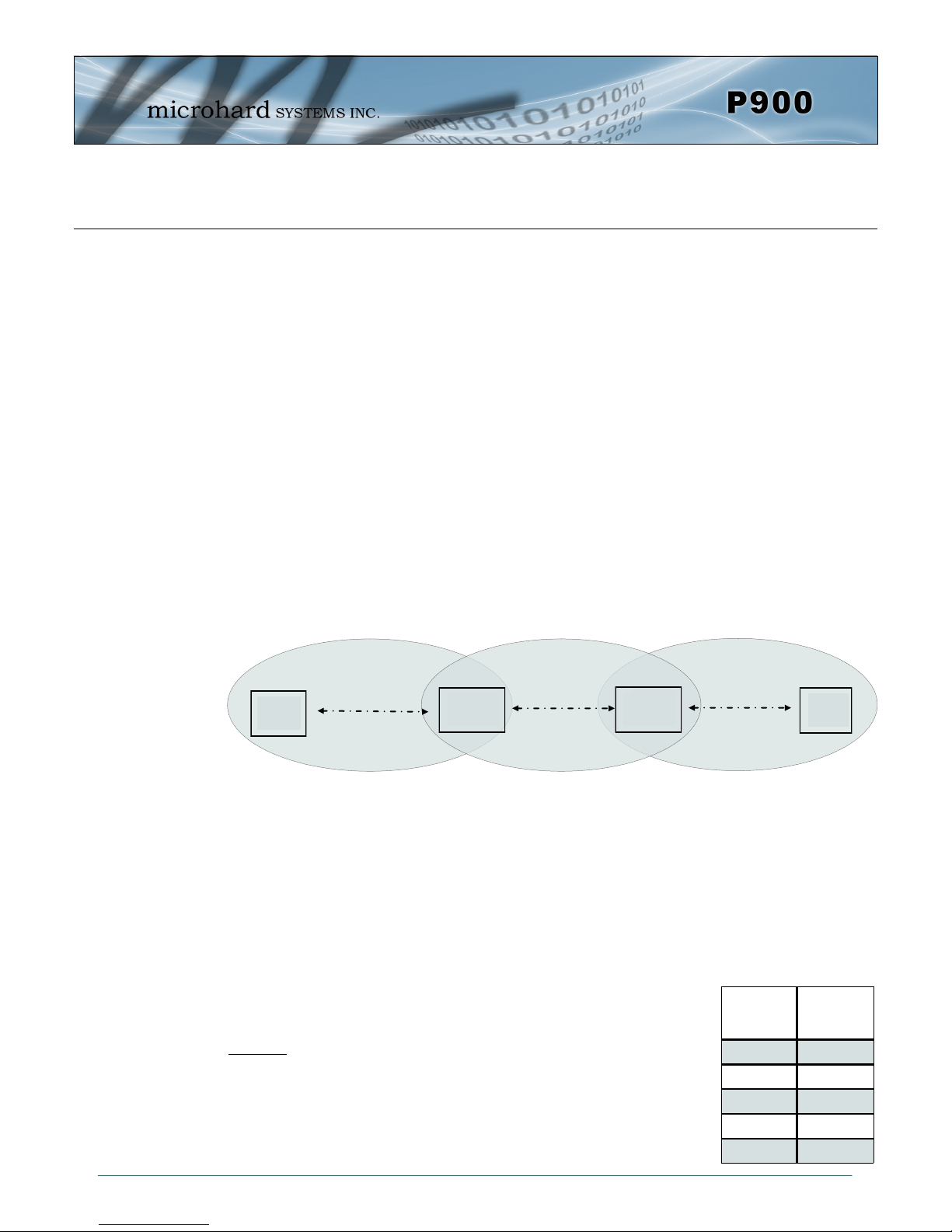
5.0 Point to Multipoint Configuration
5.2.6 Hop Patterns
Frequency Hopping modems hop from frequency to frequency to allow for multiple networks to share
the same frequency spectrum. The pattern at which the modems hop is known as the hopping pattern.
In the Pico Series modems the hop pattern is pseudo-randomly generated using a complex combination
of the Network ID (S104), Register S106 (or S206), and S180 (or S181), which define which channels
are to be included in the calculation. This ensures that no two networks have the same hopping pattern,
which would cause interference and collisions.
Register S106: The primary Hop Pattern selects the hop pattern to use between a Master or Repeater
to communicate with its associated units. The value set in this register should be the same for each unit
that is to communicate with the specific Master or Repeater. A slave will automatically discover the hop
pattern of its Master/Repeater.
S106 = 0 - Primary Hopping Pattern
S206 = 1 - Secondary Hopping Pattern
Register S206: The Secondary Hop Pattern selects a orthogonal, or different, hop pattern with nonoverlapping channels used by repeaters to communication with its’ associated units.
The following illustration should help to describe how to provision the hop patterns in systems with repeaters.
Primary Hop
Pattern
Master
Repeater
S106 =0 S106 = 0
S206 = 1
Drawing 5-5: Hop Pattern (PMP)
Secondary
Hop Pattern
Slave
Repeater
S106 = 1
S206 = 2
Primary Hop
Pattern
Slave
S106 =2
FCC requires that FHSS systems hop on 50 different channels within the 900 MHz ISM Band. The
maximum time spent on any one channel must not exceed 400ms.
To calculate the center frequency represented by each channel only the starting frequency and the size
of each channel (Channel Bandwidth) need to be known. For the 900 MHz ISM
Band, the starting frequency is 902.4 MHz, and the Channel Bandwidth is dependent on the current link
rate.
Freq channel n = 902.4+ ((n-1) x BW) MHz.
Example: Channel 75 @ 172 kbps = 902.4 +((75-1) x 0.250) MHz
902.4 + (74 x 0.250) MHz
902.4 + 18.5 MHz
920.9 MHz
Link Rate
(bps)
57600 100
115200 200
172800 250
230400 280
276480 350
Channel
Bandwidth
(kHz)
© Microhard Systems Inc. Confidential 78
Page 79

5.0 Point to Multipoint Configuration
Hop Zones
Register S180: Hop Zone and S181: Secondary Zone, select the available frequency zones used by
the Pico Series, as there may be times when multiple systems are deployed within close proximity, or
there may be outside interference or noise that requires sections of the available spectrum to not be
included in the Hop Pattern generation.
S180 = 0 - Primary Zone (0=Use Entire 902-928 ISM Band)
S181 = 0 - Secondary Zone
The Primary Hop Zone, S180 is applied to the Primary Hop Pattern (S106). The Secondary Hop Zone,
is applied to the Secondary Hop Pattern (S206), when determining the hop pattern for each segment of
the system.
Several Hop Zones are predefined by querying the S180 Register as seen below. The ranges listed are
the frequency ranges that are available to create the hop table. Using Hop Zones several frequency
Bands can be excluded. Also if multiple systems are being deployed within close proximity, Hop Zones
can be used to minimize overlap in the frequencies used to populate the Hopping Pattern.
© Microhard Systems Inc. Confidential 79
Image 5-8: Hop Zones
Page 80

6.0 Register/Command Reference
6.1 AT Commands
Appendix B is a quick reference for the available AT commands; in this sub-section are details regarding
the most commonly used. To invoke an AT command, enter Command Mode, then type AT<command>
[Enter]. Most AT commands have a help string that can be seen by typing AT<command><space>/?
[Enter].
If changes were made to
the modem’s
configuration and it is
intended that those
changes be saved to nonvolatile memory, do so
with the AT command
’&W’ prior to placing the
modem online.
A Answer
Upon completion of tasks being done with the modem in Command Mode, invoking this command will place the
modem back ‘online’ (into Data Mode).
g, G Spectrum Analyzer
This is a very useful feature of the P900. ATg or ATG will provide a display of signal levels received within the
operating environment and frequency range of the modem under test. ATg averages 256 samples, ATG 16,000.
Invoking the ATg command causes the P900 to s weep the operating band and provide a display of both the mean
and peak signal levels, in dBm, found on each channel.
The ‘graphical’ display is limited from –110dBm to –53dBm, and is in 1dB increments. Ignore the leftmost asterisk in
calculations (as below).
How to interpret the display (example):
...
ch 78 -137dBm * No signal was measured on channel 78.
ch 80 -105dBm ******... Mean signal level: -(110-5 (asterisks)) = -105dBm
... Peak signal le vel: -(110-5 (asterisks) -3 (dots)) = -102dBm
For the P900 Channel 1 is at 902.4MHz (for North America, varies by country & link rate), with subsequent channels
in increments dependent on the link rate. Therefore, to calculate the frequency of channel n: (BW = Channel
Bandwidth in MHz)
Freq channel n = 902.4+ ((n-1) x BW) MHz.
Link Rate
(bps)
57600 100
115200 200
172800 250
230400 280
276480 350
Channel
Bandwidth
(kHz)
In Identification
The I command returns information about the P900. Use ATI /? for a list of current options.
© Microhard Systems Inc. Confidential 80
0 User string. Use ATI0=<string> to save the string.
1 Product Code
2 Firmware CRC check
3 Product Identification (Firmware Version)
4 Firmware Date
5 Firmware Copyright
6 Firmware Time
7 MAC Address
11 Statistics
18 Error log
19, 20 Mesh Timing information.
255 Factory-Configured Options listing
Page 81

6.0 Register/Command Reference
ATlogin Login
AT Login can be used to enable a password prior to accessing command mode and changing any configuration
parameters. The modem must be restarted before settings will be enabled.
Image 6-1: AT login
ATM (Mesh) Main Menu
The Main Menu for Mesh diagnostics provides a user with useful information about Mesh such as the current routing
table, routing logs and errors. To access the menu use the ATM <enter> command.
Image 6-2: Mesh Diagnostics Main Menu
For more information about the Mesh Menu contact Microhard Systems for a detailed application note.
© Microhard Systems Inc. Confidential 81
Page 82

6.0 Register/Command Reference
N Advanced Spectrum Analyzer
The Advanced Spectrum Analyzer feature provides for a very detailed analysis of a particular area of the radio
frequency spectrum within which the P900 operates.
The specific start (of scan) and stop frequencies, along with step (increment) size and dwell (on frequency) time are
user-definable.
Following is the format for the ATN command:
In Command Mode
where
Example:
Note: Be sure to enter spaces as shown in the format detailed above. Use ATN /? For help.
ATN F
F
start
F
stop
S = step increment in kHz (from 1-1000)
D = dwell time in ms (from 1-1000)
ATN 905.250 908.500750 25 100
S D[Enter]
start Fstop
= start frequency in MHz (including 0-6 decimal places)
= stop frequency in MHz (including 0-6 decimal places)
&Fn Load Factory Default Configuration
Loading Factory Default settings allow for quick configuration of systems
by setting a known starting point with factory recommended s ettings for
each type of unit. The Factory settings change all settings required to
initiate default communication with other unit types.
Mesh Primary Coordinator - Each Mesh network must have a primary
coordinator. The primary coordinator provides the synchronization for the
network.
Mesh Secondary Coordinator - Secondary coordinators c an be deployed
to extend the range of the Mesh network. Each device on a Mesh network
must have LOS (Line of Sight) with either a Primary or Secondary
Coordinator.
Mesh Remote (Slave) - Any device on the network that is not a Primary or
Secondary Coordinator, generally attached to end devices. Can also be
used to perform routing tasks if enabled.
Master (PMP/PP) - Only one per network. In PP/PMP network types (see S133) data either originates at, is destined
to, or passes through the Master.
Repeater (PMP/PP) - May act simply as a ‘Repeater’ to store and forward data to/from an upstream unit to/from a
downstream unit (e.g. when there is a long distance between units), or, may act as a Repeater/Slave in which case
the above function is performed AND the unit may also exchange data as a Slave within the network.
Slave (PMP/PP) - Interfaces with remote devices and communicates with Master either directly or via Repeater(s).
Values
1 Mesh Primary Coordinator
2 Mesh Remote
3 Mesh Secondary Coordinator
7 PMP Master
8 PMP Slave
9 PMP Repeater
10 PP Master
11 PP Slave
12 PP Repeater
13 PMP Master 57k
14 PMP Slave 57k
&V View Configuration
Displays S Register names and current values. AT&V1 displays a complete set of user parameters for advance
users.
&W Write Configuration to Memory
Stores active configuration into the modem’s non-volatile memory. Any changes made to the Pico Series must be
written to NVRAM using the AT&W command (AT&WA will write the changes & set unit in online mode)
© Microhard Systems Inc. Confidential 82
Page 83

6.0 Register/Command Reference
6.2 Settings (S) Registers
The majority of modem configuration is done via the Settings (S) Registers.
Section 4.0 provides configuration detail related to operating modes and network topologies; this section
examines each S register in detail for reference or advanced/custom networks. Appendix C is a quick
reference for the S register options.
In the following descriptions, default settings (where applicable) are in boldface. In Command Mode,
Query format: ATS<S register #>? [Enter]
Change format : ATS<S register #>=<value> [Enter]
Help format: ATS<S register #><space>/? [Enter]
S0 Power-up Mode
Can be used to s elect the mode in which the unit powers up. May be useful for
users who need to configure that modem at each power up. W hen used with
the login password, can prevent the unauthorized use of the modem.
S2 Escape Character
Escape character (0-255) that is used in escape detection to put the modem
offline. Entered as a decimal number, the default of which is 43 which is the
value for the ‘+’ ASCII character. Setting to zero disables escape detection.
Note: It must be set to the default to use the M icrohard AT Command Firmware
Upgrade Utility.
S80 (MESH) Transmit Profiles
In Mesh, coordinators use automatic ranking (if enabled by S220) to logically
separate networks, ensuring that the shortest path to the Primary Coordinator is
achieved. Also to ensure that modems do not erratically associate to multiple
coordinators. Once ranked, TX Profiling can be used to split the bandwidth to
allow diff erently ranked units opportunity to send data during assigned frames.
Refer to TX Profiling & Ranking in Section 3.
Profiles:
0: 0xF,0xF,0xF,0xF,0xF,0xF,0xF,0xF,0xF,0xF,0xF,0xF,0xF,0xF,0xF,0xF
1: 0x1,0x2,0x1,0x2,0x1,0x2,0x1,0x2,0x1,0x2,0x1,0x2,0x1,0x2,0x1,0x2
2: 0x1,0x2,0x2,0x2,0x2,0x2,0x2,0x2,0x2,0x4,0x4,0x4,0x4,0x8,0x8,0x8
3: 0x1,0x2,0x2,0x2,0x2,0x2,0x2,0x2,0x1,0x2,0x2,0x2,0x2,0x2,0x2,0x2
Values
0 - In command mode
1 - In data mode (default)
Values (0-255)
43 (+)
0 disables escape detection
Values (0-3)
0
S81 (MESH) CS Threshold
The P900 uses CSMA (Carrier Sense Multiple Access) to determine if the
channel is available. The Carrier Detect Threshold is used to set the measured
level in which the signal is deemed as a valid carrier signal or outside noise or
interference (noise floor). The value represented by S81 is in –dBm. A value of
Zero (0) disabled CSMA. See Section 3 for more information.
© Microhard Systems Inc. Confidential 83
Values (0 to –255 dBm)
60
Page 84

6.0 Register/Command Reference
S83 Records TTL
The P900 keeps record of all other modems it has heard from. This information
may be useful to advanced users in s ystem testing and troubleshooting. The
RSSI in the records is averaged over the last 8 measurements. Every time a
modem is heard from its record is renewed. The ‘Time To Live’ parameter
defines how quickly entries get aged and deleted if not renewed. The range is
10 to 65535 seconds. The default is 30 seconds. The content of the records
can be viewed through the menu, see the ATM command for more information.
Values (10 to 65535)
30
S85 (PP/PMP) Distance to Master
The distance from a slave (repeater) to its master (repeater). This is used by
slaves and repeaters in PMP and PP modes. 0 to 255km, the default is 3km.
Long distance causes propagation delays, S85 should be set accordingly.
Values (0 to 255km)
3
S86 (PP/PMP) Distance From Master
The distance from a master (repeater) to its farthest slave (repeater). It is used
by the Master and repeaters in PMP and PP modes. 0 to 255km, the default is
3km. A setting of 255 means no slaves will be transmitting any packets - one
way transmission from the master.
Since the timing on slaves (relative to master) is already offset by the propagation delay, transmitting data back from
slaves to the master causes doubling of the delay when viewed on the master. W hen distances are long and not
accounted for by setting S86 accordingly, a packet from far away slaves may arrive too late for the master to receive
it before the hop interval expires. W hen there are no slaves that may transmit data back to the master (one way
transmission), the master may use its bandwidth more effectively by not reserving time in the hop interval for slave’s
data. S86=255 is a special value to indicate to the master that slaves will not transmit back.
IMPORTANT: Slaves in PP mode acknowledge the master’s data, therefore in PP mode S86 must be configured
properly even if there is no user data coming from the slaves.
Values (0 to 255km)
3
S87 (MESH) Enable S105 as MAC
Enables using S105 as modem’s units address in Mesh. Can be useful in
installations where many modems send data to a central location. If the
Destination address of those modems is set to match a unique MAC address of
the receiver, and the receiver fails and needed to be replaced, it may be difficult
to reprogram the destination address S140 on all radios to the new MAC
address of the replaced radio.
This feature can also be useful in fleet management applications, or roaming
mesh networks. W ith roaming, a sink of data in each network will have the
same address, for example UA = 1. In this case a roaming remote will have its
DA = 1 and will always send data to a sink regardless of which network the
remote is connected to in any given time. The range is 1 - FFFE (of S105), the
value must be entered as a hex number.
© Microhard Systems Inc. Confidential 84
Values (selection)
0 - Disable (default)
1 - Enable
Page 85

6.0 Register/Command Reference
S101 (MESH) Operating Mode
The Operating mode defines the role in the network a unit plays. A P900
modem may be configured for any role required within a radio network. This is
convenient for reasons of familiarity with any/all units, as well as for hardware
sparing purposes.
Remote: Any unit that is not a coordinator.
Coordinator: Every Mesh network requires a primary coordinator. Coordinators are used to synchronize the
network. If additional coverage is required additional secondary coordinators can be deployed.
Secondary Coordinator: Secondary Coordinators can be deployed to extend the network and to provide LOS
for geographically challenged remotes.
Standby Coordinator: Can be used to take over the duties of the Primary Coordinator to provide redundancy.
Values
2 Slave (Remote)
4 Coordinator
5 Secondary Coordinator
6 Standby Coordinator
S101 (PP/PMP) Operating Mode
The Operating mode defines the role in the network a unit plays. A P900
modem may be configured for any role required within a radio network.
Master: Only one per network. In PP/PMP network types (see S133) data
either originates at, is destined to, or passes through the Master.
Repeater: May act simply as a ‘Repeater’ to store and forward data to/from an upstream unit to/from a downstream
unit (e.g. when there is a long distance between units), or, may act as a Repeater/Slave in which case
the above function is performed AND the unit may also exchange data as a Slave within the network.
Slave: Interfaces with remote devices and c ommunicates with Master either directly or via Repeater(s).
Values
0 - Master
1 - Repeater
2 - Slave (Remote)
Note: Most PC’s do not
readily support serial
communications greater
than 115200bps.
S102 Serial Baud Rate
The serial baud rate is the rate at which the modem is to communicate with the
attached local asynchronous device. This value must match the PC or serial
device that is connected to data port on the P900.
When forcing a module to Command Mode the data port will temporarily
communicate at the default value. When the P900 is retuned to Data Mode, the
serial port settings are returned to those specified in S102 and S110.
Values (bps)
0 230400
1 115200
2 57600
3 38400
4 28800
5 19200
6 14400
7 9600
8 7200
9 4800
10 3600
11 2400
12 1200
13 600
14 300
S103 Wireless Link Rate
This register determines the rate at which RF communications will occur over a
given network. All modems within a particular network must be configured with
the same wireless link rate. Faster link rates result in greater throughput,
however, f or each ’step’ increase in link rate, there is an approximately 1dB
reduction in sensitivity.
Values (bps)
0 172800
1 230400
2 276480
3 57600
4 115200
© Microhard Systems Inc. Confidential 85
Page 86

6.0 Register/Command Reference
S104 Network Address (ID)
Change the default value
for the Network ID to
something unique for your
network. Do this for an
added measure of
security and to
differentiate your network
from others which may be
operating nearby.
FCC regulations allow
for up to 36dBi effective
isotropic radiated power
(EIRP). The sum (in
dBm) of the transmitted
power, the cabling loss,
and the antenna gain
cannot exceed 36dBi.
All modems in a given network must have the same Network Address. This
unique network address is not only a security feature for a particular network,
but also allows other networks - with their own unique network address - to
operate in the same area without the possibility of undesired data exchange
between networks.
Values (0 - 4,294,967,295)
1234567890
S105 Unit Address
Unit address in PP and PMP modes, or in MESH if S87=1. The unit address is,
and must be, a unique identifier of each modem in a network. The address
value is 16-bits in length.
The Master has by default, and must retain, a unit address of 1; 65535 is the
broadcast address.
Values (1 - 65534)
1 in PP/PMP
1-FFFF in MESH
S106 Hop Pattern
This register, together with the Network ID and the Hop Zone, determines the
Hopping Pattern or table on which the P900 will frequency hop. This register
must be set to the hop pattern of the immediate Master/Repeater, unless
roaming is used.
Values (0 - 49)
0
S108 Output Power
This setting establishes the transmit power level which will be presented to the
antenna connector at the rear of the modem.
Unless required S108 should be set not for maximum, but rather f or the
minimum value required to maintain an adequate system fade margin.
Values (dBm (mw))
20 (100)
21 (125)
22 (160)
23 (200)
24 (250)
25 (320)
26 (400)
27 (500)
28 (630)
29 (800)
30 (1000)
© Microhard Systems Inc. Confidential 86
Page 87

6.0 Register/Command Reference
S109 (PP/PMP) Hop Interval
This register is effective only on the Master and is responsible for establishing the rate at which all modems within a
particular network change frequency (hop - from frequency to frequency).
Long hop intervals typically result in the greatest data throughput, however shorter hop intervals may decrease
latency and make the system more immune to interference.
The default setting of 20ms is satisfactory for most applications
S109 time (ms) S109 time (ms) S109 time (ms) S109 time (ms)
0 1.498 16 89.997 32 11.997 48 21.998
1 2.001 17 99.998 33 12.500 49 22.999
2 2.498 18 125.000 34 12.998 50 24.000
3 3.002 19 150.001 35 13.501 51 25.001
Hop Interval S109 should
only be changed if
recommended by
Microhard Support and/or
for specific applications!
4 3.997 20 4.500 36 13.998 52 26.001
5 4.997 21 5.501 37 14.502 53 27.002
6 6.999 22 5.998 38 15.502 54 27.997
7 10.001 23 6.501 39 16.000 55 28.998
8 14.999 24 7.502 40 16.497 56 8.335
9 19.997 25 8.000 41 17.001 57 199.997
10 29.999 26 8.497 42 17.498 58 250.000
11 40.000 27 9.000 43 18.001 59 300.002
12 50.002 28 9.498 44 18.499 60 349.998
13 59.998 29 10.499 45 19.002 61 378.997
14 69.999 30 11.002 46 19.499
15 80.001 31 11.499 47 20.998
S110 Data Format
This register determines the format of the data on the serial port. The default is
8 data bits, No parity, and 1 Stop bit. The value must match the PC or Serial
Based device that is connected to the data port.
When forcing a module to Command Mode the data port will temporarily
communicate at the default value. When the P900 is retuned to Data Mode, the
serial port settings are returned to those specified in S102 and S110.
© Microhard Systems Inc. Confidential 87
Table 6-1: Hope Interval (S109)
Values
1 8N1
2 8N2
3 8E1
4 8O1
5 7N1
6 7N2
7 7E1
8 7O1
9 7E2
10 7O2
Page 88

6.0 Register/Command Reference
S111 Packet Min Size
In a PMP system, set
S113 to the minimum
value required as,
effectively, the data
throughput from Master to
Remote is divided by 1
plus the number stored in
S113.
This is the minimum number of collected bytes in one buffer before the buffer
can be closed by the character timeout timer controlled by S116. It is
STRONGLY advised not to modify this parameter. Changing S111 may prevent
the modem from detecting the escape sequence.
Values (1 - 255)
1
S112 Packet Max Size
Determines that maximum number of bytes from the connected device that will
be encapsulated into a packet unless the character timeout timer S116 expires.
Large packet sizes may produce the best data throughput; however, a smaller
packet is less likely to become corrupted and, if it does, is retransmitted with a
lesser impact on network traffic. The default setting of 256 bytes is suited to
most applications.
Values (1 - 256)
256
S113 Packet Retransmissions
This register determines the maximum number of times that a packet will be
retransmitted (in addition to the initial transmission). Retransmissions can be
used to provide system robustness and to ensure data delivery due to noisy
environments or weak signal levels. Retransmissions should not be used as the
only means to c orrect for data collisions. Retransmissions create additional
traffic and can have a significant impact on overall throughput of a system.
Values (0 - 254)
5
S115 Repeat Interval
In Mesh S115 defines the randomness of accessing the channel (0 - 255). The
bigger the number, the less often attempts are made to access the channel,
resulting in lower collisions, but at the cost of added latency.
Values (0 - 255)
5 (Mesh), 3 (PP/PMP)
In PP/PMP S115 determines the number of slots which are available within a window of opportunity for Remote units
to submit channel requests to the Master modem. For a large number of remotes, the value of S115 should be set
relatively high: Remotes will randomly contend f or the ability to access the channel request slots. For a s mall
number of Remotes, it is advisable to keep S115 closer to the default value so as to not ‘waste bandwidth’ by
maintaining a relatively large window housing a greater-than-necessary number of channel reservation request slots.
S116 Character Timeout
Character Timeout in 1/4 of character time (10-255). Default = 10 (2.5
character time). This ‘timer’ looks for gaps in the data being received from the
local attached device. The timer is activated after the Minimum Packet Size
(S111, default 1 Byte) has been accumulated in the modem. If the timer detects
a gap in the data exceeding the Character Timeout value, the modem will
transmit the data.
The Pico will accumulate data in its buffers until either (a) Maximum Packet size (S112) has been accumulated, or
(b) Minimum Packet Size (S111) has been accumulated AND the Character timeout has expired—whichever occurs
first.
© Microhard Systems Inc. Confidential 88
Values (10 - 254)
10
Page 89

6.0 Register/Command Reference
S118 (PP/PMP) Roaming
A Master modem’s RSSI
LEDs will not illuminate to
any degree until such time
as it has received valid
packets from a
‘downstream’ unit.
This feature allows a Remote unit to synchronize with a specified ‘upstream’
unit (either Master or Repeater). The options are as follows:
S118=65535: A Remote will synchronize with an upstream unit which has
S118=1-65534 In most static (fixed) networks, where there are no Repeaters, the default value of 1 is
In networks where Repeaters are present, the value of a Remote’s S118 corresponds to the particular upstream
modem with which a particular Remote is intended to communicate, e.g. Slave UA (S105)=3 may have an S118=2,
where the modem with UA 2 is a Repeater between the Slave and the Master; the Repeater will have an S118=1.
the same network address (S104). Should that upstream
unit fail, this Remote will attempt to synchronize with
another ’upstream’ unit within the same network. This ability
is particularly well-suited to mobile applications.
maintained: All Slaves synchronize to the Master (whose unit address is 1).
Values
65535 full roaming
1-65534 specific (fixed) unit
address with which to associate
1
S123 (MESH) Average RSSI
This register displays (it is not a ’setting’) the average signal strength received
over the previous 8 hop intervals. The value in this register is also reflected in
status lines RSSI1, 2, and 3, which connect to the modem’s RSSI LEDs.
Values (dBm)
-110 to –55dBm (max reading)
S123 (PP/PMP) RSSI from Master (dBm)
In repeaters and slaves this register displays the average signal strength
received over the previous 8 hop intervals from a Master/Repeater. The value
in this register is also reflected in status lines RSSI1, 2, and 3, which connect to
the modem’s RSSI LEDs.
Values (dBm)
-110 to –55dBm (max reading)
S124 (PP/PMP) RSSI from Slave (dBm)
On the master this register displays the average signal strength received over
the previous 8 hop intervals from a Slave/Repeater. The value in this register
is also reflected in status lines RSSI1, 2, and 3, which connect to the modem’s
RSSI LEDs.
Values (dBm)
-110 to –55dBm (max reading)
S126 (MESH) Attempt Before Re-route
Number of consecutive unacknowledged transmissions before starting route
discovery in Mesh. 1-255, default = 9. W hen a route is added to a routing table
it is important that the data in the table remain current and c orrect. The S126
register sets a maximum number of attempts to reach a route before the route
is removed from the routing table and route discovery is started. See s ection 3
for more information.
Values (1-255)
9
S130 No Sync Data Intake
When enabled allows a modem to receive and keep data from the local com
port while the modem is searching for synchronization. Does not apply to
master and primary coordinator. Should normally be disabled to prevent
accumulation of stale data inside a modem.
© Microhard Systems Inc. Confidential 89
Values (selection)
0 - Disabled (default)
1 - Enabled
Page 90

6.0 Register/Command Reference
S133 Network Type
This register defines the type of network being deployed. This register must be
set to the same value on every unit in the system.
Point to Multipoint - The Master broadcasts data to all units, and all remote
units send data back to the Master. (See Section 5)
Point to Point - Point to point traffic between a Master and a Slave (with 0 or
more Repeaters in between). (See Section 4)
Mesh - A Mesh network is a network where radios can communicate with each other directly or, if required through
another mesh node, without all data being routed through a master. (See Section 3)
Mesh with Roaming - This is identical to Mesh S133=2 except a remote may join networks with different S106 and
S180. Used in roaming applications.
Values (selection)
0 - Point to Multipoint (PMP)
1 - Point to Point (PP)
2 - Mesh
3 - Mesh with Roaming
S140 Destination Address
As the name implies, this register specifies the ultimate destination for a
modem’s data.
In a Mesh system, the destination address is entered in MAC address format,
where FF:FF:FF:FF:FF:FF is broadcast. For unicast operation, the factory
assigned MAC address of the destination device must be used. Or S105 if S87
= 1.
In PMP and PP modes - the range is 1 to 65535, where 65535 is broadcast:
PMP - Master S140=65535, Remote S140=1
PP - Master S140=UA of Remote, Remote S140=1 (Master)
Values
Varies by network and unit type
S141 (PP/PMP) Repeaters Y/N
This register informs, and only applies to the Master, as to the presence of any
Repeater(s) in the network. With one or more Repeaters in the system, a
network’s throughput is divided in half.
Values (selection)
0 - no repeater
1 - 1 or more repeaters
S142 Serial Channel Mode
This register selects the s erial channel mode for the data port. The default is
RS232. In RS485 either DSR or CTS (set high) can be used to enable the
transmitter of the RS485 driver chip. If &K1 is used, CTS will control the
transmitter. Otherwise DSR does it. In this c ase the value of &S is ignored. The
RING line is set high and is normally used to enable the receiver of the RS485
driver chip.
Values (selection)
0 - RS232
1 - RS485 half duplex
2 - RS485 full duplex
S143 Sleep Mode
When set to 0 the modem is active at all times. W hen S143=1 enables sleep
mode on remotes only. Sleeps f or S144 seconds or until the rising edge of the
Wakeup_usr line. Stays on for at least S145 seconds. After that goes to sleep if
all data including over the air is sent. Upon wake up the modems will be out on
sync with the network and need time to re-synchronize. The DSR line can be
configured to indicate when the modem is asleep (DSR = 1) and awake (DSR =
0).
© Microhard Systems Inc. Confidential 90
Values (selection)
0 - Active all the time
1 - Enabled
Page 91

6.0 Register/Command Reference
S144 Sleep Time
Sleep time in seconds. If Sleep mode is enabled (S143), modem will go to
sleep for S144 seconds or a rising edge of the W akeup-user line.
Values (2 - 65535)
60
S145 Wake Time
Wake time in seconds. If Sleep mode is enabled (S143), modem will stay
awake for S145 seconds if all conditions of S143 are met.
Values (1 - 65535)
10
S146 Tx Done timeout, 1/4
Normally used with Modbus RTU protocol which requires a 3.5 character delay
between packets output on the c om port. Range is 0 to 255, default is 14 (3.5
chars). This register along with Modbus RTU setting of S217 can be used to
insert a gap between individual packets coming out of the serial port even in
non-Modbus applications.
Values (0 - 255)
14
S151 (MESH) Quick Sync Packets
At system startup when coordinators first come online, they send out a number
of quick sync packets, defined by register S151, used to quickly attain network
synchronization. Each quick sync packet is sent on a random channel listed in
the hop pattern. The more sync packets sent, the quicker network
synchronization occurs, but at a cost of delayed data transmission. The lower
the number of packets sent, the less likely the entire network will synchronize
during the quick sync process, resulting in slower overall synchronization.
Values (5 - 65534)
500
S153 Address Tag
Prepends each packet received from the radio with 10 bytes of the following
data:
Type 1: First 2 bytes - size (high byte first), one byte - RSSI, one reserved byte
(0x00), last six bytes - source unit address (high byte first).
Values (selection)
0 - Disable (default)
1 - Type 1
© Microhard Systems Inc. Confidential 91
Page 92

6.0 Register/Command Reference
S158 FEC (Forward Error Correction) Mode
If throughput is not of
primary concern and there
is an emphasis on
providing the most robust
data communications,
FEC should be
considered.
A number of FEC schemes are available with different coding rates.
FEC consumes significant bandwidth: depending on which coding rate is
chosen, a number of c oding bits are transmitted along with the ‘data’ bits. In
‘noisy’ or long-range communications environments, FEC may effectively
increase throughput by decreasing the amount of packet retransmissions which
would otherwise be required.
Communications range may also be extended with the use of FEC: at a certain
distance where data would otherwise be unacceptably corrupted, employing
FEC may be all that is required to maintain the integrity of that data at that
distance.
Types of FEC available within the P900:
Hamming (7,4) : Information rate 0.5,
corrects 1 out of 7 bits
Hamming (15,11) : Information rate 0.66,
corrects 1 out of 15 bits
Hamming (31,24) : Information rate 0.75,
corrects 1 out of 31 bits
Binary BCH (47,36) : Information rate 0.75,
corrects 2 bits
Golay (23, 12, 7) : Information rate 0.5,
corrects 3 bits
Reed-Solomon (15,11) : Information rate 0.687,
corrects 2 nibbles
Values
0 No FEC
1 Hamming (7,4)
2 Hamming (15,11)
3 Hamming (31,24)
5 Binary BCH (47,36)
6 Golay (23,12,7)
7 Reed-Solomon (15,11)
S159 Encryption Mode (AES)
AES encryption is only available in models delivered as –AES. This is a
factory configured option that can only be loaded and enabled at the
factory at time of assembly. The use of AES encryption, and export laws
governing AES, vary from country to country, contact Microhard Systems
Inc. for more information.
AES (Advanced Encryption Standard) provides an extremely strong level of
encryption for data for security of wireless data communication.
Values
0 No encryption
1 AES 128 bit
2 AES 192 bit
3 AES 256 bit
Up to three levels of AES are available, 128 bit, 192 bit and 256 bit. Only the specific options enabled by the factory
will be available Once a level of AES is chosen using register S159, the encryption key must be entered. The same
AES setting and encryption key must be entered on every modem in the network.
The size of the key is dependant of the level of AES:
128bit AES: 16 Byte Encryption Key
192bit AES: 24 Byte Encryption Key
256bit AES: 32 Byte Encryption Key
The encryption key can be entered in registers S107 or S177 as they share the same key array for encryption. S107
(Static Mask) is used to enter in up to 32 printable characters (ASCII). If using 128 or 192 bit AES, any character
entered after 16 or 24 bytes respectively will be ignored. If less than the required number of characters is entered, 0’s
will be appended to fill the encryption key array.
To improve the strength of the key, S177 can be used to enter 16-32 bytes (dependant of the AES type) of binary
non-printable characters. This register requires the appropriate number bytes to be entered. In other words, if you are
using AES256, S177 requires 32 bytes of data to be entered. A binary file can be transferred to the modem using a
terminal program after a ATS177= command has been invoked.
© Microhard Systems Inc. Confidential 92
Page 93

6.0 Register/Command Reference
S163 CRC check on diag port
Enables CRC16 checking of received data on local diagnostic port. Note that
even if disabled, the incoming data must have two dummy bytes transmitted in
place of crc bytes. Disabling CRC check is only advisable during
troubleshooting of the user’s diagnostic requests.
Values (selection)
0 - Disable
1 - Enable (default)
S177 Binary Encryption Key
When using AES encryption, S177 can be used to define the encryption key in
binary. The type of AES used defines the minimum number of binary bytes that
need to be entered. See S159 for more information.
Values (Binary Bytes)
16 - 32 Bytes (AES type
dependant)
S180 Hop Zone
S180 will allow the use of hopping zones to restrict the hopping table to specific
segments of the 900 MHz ISM band. The default is to populate the hopping
pattern/table using channels or frequencies from the entire 900MHz ISM band.
Additional zones can be seen by displaying help for the S180 register.
Values (0-10)
0 - Use entire ISM band
S181 (PP/PMP) Secondary Hop Zone
Used on PP and PMP Repeaters, S181 will allow the use of hopping zones to
restrict the secondary hopping pattern to specific segments of the 900 MHz ISM
band. Any downstream units connected to this will need to have their S180
(Primary Hop Zone) set to same value as the Secondary Hop Zone of the
Repeater they are connected to.
The default is to populate the hopping pattern/table using channels or
frequencies from the entire 900MHz ISM band. Additional zones can be seen
by displaying help for the S181 register.
Values (0-10)
0 - Use entire ISM band
S183 (PP/PMP) DCD Pulse Period
The period of DCD pulses on synchronized slaves in &C3 mode. Minimum
value = 1, Max value = number of channels in a hop pattern minus one. The
default is 5.
S183 = 1 - DCD will pulse every hop interval, if S183 = 3 - every third, etc. The
counter starts at hop index 0. It is used in some applications to generate
common synchronization on many slaves. W ith the default setting of 5 and the
hop interval of 20ms, each slave will synchronously generate a pulse of
approximately 3ms every 100ms.
© Microhard Systems Inc. Confidential 93
Values
5
Page 94

6.0 Register/Command Reference
S184 (MESH) Data Time to Live
Data time to live in 10ms ticks. Used to age data in mesh networks. The default
is 65535 (never age).
Values (1 - 65535)
65535
S206 (PP/PMP) Secondary Hop Pattern
This register, together with the Network ID and the Secondary Hop Zone,
determines the Secondary Hopping Pattern which a P900 Repeater will use to
synchronize and communicate with downstream units. The S106 (Primary H op
Pattern) register must be set to the same value on each repeater/slave that is
downstream of this unit.
Values (0 - 49)
1
S214 (MESH) Number of Aloha Slots
This register defines the number of aloha slots available in a Mesh Frame. A
slot is a set period of time required to transmit the shortest packet (RTS, CTS,
ACK).
Increasing the number of aloha slots allows more time for a modem to transmit
data during a Mesh Frame. The number of aloha slots directly impacts the hop
interval, the more aloha slots, the more time to transmit data, but also the
longer the system sits on a single frequency. Reducing the number of aloha
slots creates a shorter hop interval which results in a system more immune to
interference, but too short an interval may disable communication if devices do
not have time to transmit.
Values (1-255)
60
S215 (MESH) Number of Mesh Sync Slots
This register defines the number of sync slots available in a Mesh Frame. The
valid range is 1 - 10, with a default of 1. In systems with many coordinators,
additional slots may be required to avoid collisions. Register S216 can also be
used to provide randomness in sending sync packets to avoid collisions.
S215 must be set to the s ame value for each modem on the network or the unit
will not synchronize.
Values (1-10)
1
S216 (MESH) Mesh Sync Duty Cycle
Defines how often the coordinator transmits sync packets (1-100). After each
sync packet transmission the c oordinator picks a random number from 1 to the
value in S216 and transmits the next packet in this slot. 1 - every sync slot, 2—
on average once every 1.5 slots, 3 - on average once every 2 slots etc.
© Microhard Systems Inc. Confidential 94
Values (1-100)
3
Page 95

6.0 Register/Command Reference
S217 Protocol Type
Defines how data is output on the local serial port. When Modbus RTU is
enabled, there is a delay between the packets coming out of the serial port. The
register S146 defines the delay between individual packets.
Values (selection)
0 - Transparent Serial (default)
1 - Modbus RTU
S218 (MESH) Input Framing
Input Framing Type. Controls how the modem treats data coming to its s erial
port. Allows the destination address to be embedded into the data stream,
which is automatically stripped by the P900 before transmitting the packet.
0 - Transparent Serial (Default)
1 - Destination Address (DA) is in first six bytes (high byte first) of the
packet. The modems strips these six bytes and doesn't transmit them. For
example, if the DA is 01:23:45:67:89:AB then the high byte is 0x01,the
lowest byte is 0xAB. Note that the max size of the data itself in this case is
S112 minus 6. If S112 = 256 then the max data size is 250 bytes.
Values
0
S219 (MESH) Routing Request TTL
Routing Request Timeout in 10ms ticks. (1-10000). The default is 10, which is
100 msec. This defines how long a unit will wait for a Routing Request to
provide possible routes. D uring this time no other data may be sent from the
unit. Setting this value too low may not give the system enough time to report
the best path, alternately, a value too high may create latency in the system as
it waits for the TTL to expire before allowing data transmission, although it has
already received the best path.
Values (1-10000)
10 (100ms)
S220 (MESH) Mesh Coordinator Rank
Used with T x Profiles. Can be set to 0-3 or 255. Value of 255 (default) is for
automatic ranking.
Values (selection)
0-3 or,
255
S221 (MESH) Mesh TDMA Slot to Tx
Aloha slot number in mesh TDMA in which the modem will start its transmission
in Tx On Slot channel access mode S244 = 2. 1-255 (default is 1). See the app
note for Mesh TDMA.
Values (1 - 255)
1
S222 (MESH) Roaming Mode
When roaming is disabled a mesh radio will synchronize only to a coordinator
with the matching set of S106 and S180. When roaming is enabled the modem
will synchronize with any valid coordinator.
Values (selection)
0 - Disabled
1 - Roaming on Z one/Pattern
© Microhard Systems Inc. Confidential 95
Page 96

6.0 Register/Command Reference
S223 (MESH) Routing
Each unit in a Mesh
network has a unique MAC
Address. Unicast Data with
a destination address of the
primary Coordinator will
NOT be automatically
routed to the Standby
Coordinator.
Compression was
introduced in firmware
v1.10. Older versions of
firmware will not be
compatible with v1.10
unless S225 is disabled
or older units are
upgraded.
This register is used to enable or disable Mesh Routing function of the modem.
Whenever coordinators are added to a system, routers are typically required in
a network. Any unit in a Mesh network can be used to perform routing tasks.
Although it is a good idea to have more than a s ingle router, too many routers
may create unnecessary traffic in the system. See Section 3 for additional
information.
0 - Disabled - Disabled by default
1 - Enabled - Routing can be enable on any unit, but the more units
performing routing tasks, the more routing traffic generated.
Values
0 - Disabled
1 - Enabled
S224 (MESH) Standby Trip Level
Mesh Standby Coordinator sync level at which it becomes the primary
coordinator. 0 - 255, Default = 20.
This register works with the Sync Timeout (S248) on the Primary coordinator to
monitor the s ync level to determine when the Primary Coordinator has f ailed.
The Sync Timeout sets a counter (set by S248 on the Primary coordinator and
propagated in sync packets) that counts down each time a frame is received
that does not contain sync data from a coordinator. If the unit receives s ync
data the counter is reset, if the counter reaches zero - the unit loses sync.
The Standby Trip Level (S224) is designed to be able to transition a Standby
Coordinator to a Primary Coordinator before the network loses s ync. This is
accomplished by watching the counter set by S248 and triggering at the level
set by S224.
Values (0-255)
20
S225 Compression Mode
Using compression may improve overall performance of the modem. Default is
enabled.
Values
0 - Disabled
1 - Type 1 Enabled
S232 Max Buffer in Storage
Maximum number of buffers from the local com port. 1 to 255, default 200.
Used to limit the amount of storage the modem will allocate to incoming user’s
data. Each buffer is S112 number of bytes. With S112=256 (default) and
S232=200 (default) the modem can store up to 51200 bytes.
© Microhard Systems Inc. Confidential 96
Values (1-255)
200
Page 97

6.0 Register/Command Reference
S234 (PMP) Master Ch. Req. Timeout
After the master releases the channel, it will wait f or the S234 number of hop
intervals to allow the slaves to send channel requests before the master
arbitrates the channel.
When there are many slaves that may want to request the channel at the same
time, setting this register to a bigger number will help ensure that the channel
arbiter in the master will allocate the channel fairly - new modems will be given
higher priority over modems that were recently allocated the channel.
Values (1-254)
1
S235 (PP) PP Routing TTL, sec
Routing Time to Live in seconds. (1-65535). Defines the aging interval for
routing information in PP Mode.. 65535—never age. Default is 30 seconds.
Values (1-65535)
30
S236 Max Buffer Out Storage
Maximum buffer out storage. Limits the number of buffers waiting to be output
to the user on COM1 (1-65535), default is 255. Normally should not be
changed.
Values (1-65535)
255
S244 (MESH) Channel Access Mode
Channel Access Mode. This register defines how devices access the channel
when they have data to transmit.
0 - Aloha - Units use Carrier Sense (CSMA) to access the channel, if
available, and send data. Register S115 can be set to
configure the randomness at which devices access the
channel to avoid collisions. Default for coordinator.
Values
0 - Aloha
1 - RTS/CTS
2– TDMA
1 - RTS/CTS - When units wish to transmit, they request a channel (RTS) from the associated coordinator. The
Coordinator will respond immediately (CTS) if the channel is successfully allocated. Default for
secondary coordinators and remotes.
2 - TDMA - Transmission on slot. See S221.
S245 (MESH) Cost of Hop
Cost of one hop in mesh routing. When choosing the best route, the cost of
each route must be considered. Cost of Hop allows a user to influence the
relationship between the c ost of RSSI and the Cost of Each hop. See Section
3.2.7 Routing for a detailed explanation.
S247 Country Code (Read Only)
This register shows the currently f actory s et country code. This is a read only
register and can only be modified at the factory.
© Microhard Systems Inc. Confidential 97
Values (0-255)
100
Values (N/A)
Read Only, Varies
Page 98

6.0 Register/Command Reference
S248 Sync Timeout
To remain synchronized to the network a unit must receive sync data
occasionally from a coordinator or master. The Sync Timeout defines the
number of frames (Mesh) or hops (PMP/PTP), before losing sync completely.
The sync timeout works like a counter that decrements with each frame or hop
interval where sync data is not received. When valid sync data is received the
counter is reset to the value set in S248, if the counter reaches zero, the unit
will lose sync.
In MESH is only set on Primary Coordinator and propagated in sync packets.
Values (4-65534)
100 (Mesh)
512 (PP/PMP)
S249 (PMP/PP) Pkts per hop tx limit
Limits the number of packets a modem can send in one hop interval (1-255).
Default - 255 (unlimited). Normally should be left unchanged.
Values (1-255)
255
S250 (PMP) Master Bandwidth, %
Sets a limit on bandwidth available to the master in PMP mode when the
channel is allocated to a slave.
Values (0-100%)
50
S251 (PMP) Master Hop Allocation Timeout
In PMP mode S251 defines the channel release timeout in hop intervals. (1-
255). Normally a slave must release the channel by s ending a channel release
packet. If slave stopped communicating with master and didn't release the
channel, the master will wait for S251 hop intervals before de-allocating the
channel. Normally should be left unchanged.
Values (1-255)
10
S252 (PMP) Slave Ch Allocation Timeout
Channel Allocation Limit f or slave, packets (1-255). Defines a number of
packets a slave can transmit before releasing the channel. 255 - no restrictions.
Default - 10.
© Microhard Systems Inc. Confidential 98
Values (1-255)
10
Page 99

6.0 Register/Command Reference
6.3 Serial Interface Commands
A number of register settings are specifically related to the serial data interface. Some, which have
been discussed previously, include:
S102 Serial Baud Rate determines the rate of communication between the modem and
the local device
S110 Data Format defines the data, stop, and parity bit count
Also, there are AT commands which effect the configuration of the module, specifically with respect to
the handling of data at the RS-232 interface:
&C Data Carrier Detect (DCD)
&D Data Terminal Ready (DTR)
&K Handshaking
&S Data Set Ready (DSR)
Software flow control
(XON/XOFF) is not
supported.
&Cn Data Carrier Detect (DCD)
Controls the module’s DCD output signal to the attached device.
Determines when the DCD line is active.
&C0 - DCD always on
&C1 - DCD on when synchronized
&C3 - In PP/PMP systems, slaves/repeaters provides an external global
synchronization pulse. See S183
&C4 - In Mesh - DCD as carrier detect. Active (0V CMOS) when carrier is
detected. Uses CS threshold S81
&C5 - In Mesh - DCD as carrier detect. Opposite to &C4 - active
when there is no carrier
*DCD always on when module
configured as a Primary
Coordinator or Master
Values
0 DCD always on
1 DCD on when synchronized*
3 PP/PMP Sync Pulse
4 Mesh DCD active when carrier
5 Mesh DCD not active w/carrier
&Dn Data Terminal Ready (DTR)
Controls the action that the module will perform when the DTR input
line’s state is modified.
Values
0 DTR ignored
2 DTR disconnects and switches to
command mode
&Kn Handshaking
Enables or disables hardware handshaking.
Values
0 Handshaking disabled
1 CTS Control Transmitter of RS485
driver chip.
3 RTS/CTS handshaking enabled
&Sn Data Set Ready (DSR)
Controls the module’s DSR line and determines when it is active.
In RS485 modes DSR controls the transmitter of the RS485 driver chip
unless &K1 is used. High level enables the transmitter.
© Microhard Systems Inc. Confidential 99
Values
0 DSR always on
1 DSR = 0 in data mode, 1 command
mode
2 DSR = 0 when awake, 1 asleep
Page 100

7.0 Installation
The are a number of factors to consider when preparing to deploy a radio network, several of
which have been touched-upon or detailed elsewhere within this manual. Following is a listing of a number of factors, in no particular order:
Network Topology
The P900 currently supports Mesh, Roaming Mesh, Point to Point, and Point to Multipoint
topologies.
The installation,
removal, or
maintenance of any
antenna system
components must be
undertaken only by
qualified and
experienced
personnel.
Throughput
The P900 is capable of up to 230.4kbps asynchronous baud rate. The network topology has
an effect on how this available throughput is ‘shared’ between all nodes on the network.
Distance
The physical distance between the modems dictates such things as required antenna performance and heights. When contemplating antenna types, keep in mind the directivity
(omnidirectional or directional) of the antennas being used.
Terrain
Along with distance, the terrain is a very important consideration with respect to antenna
height requirements. The term ‘line-of-sight’ (LOS) refers to being able to ‘see’ one location
from another - a minimum requirement for a radio signal path. In addition to LOS, adequate
clearance must also be provided to satisfy ‘Fresnel Zone’ requirements - an obstruction-free
area much greater than the physical LOS, i.e. LOS is not enough to completely satisfy RF
path requirements for a robust communications link.
Transmit Power
Having read thus far through the factors to be considered, it should be clear that they are all
interrelated. Transmit power should be set for the minimum required to establish a reliable
communications path with adequate fade margin. Required transmit power is dictated primar-
ily by distance, antenna type (specifically the ‘gain’ of the antennas being used), and the re-
ceive sensitivity of the distant modem. Cable and connector losses (the physical path from
the modem’s ‘antenna connector’ to the antenna’s connector) must also be taken into ac-
count.
Receive Sensitivity
The Pico Series has exceptional receive sensitivity, which can produce a number of benefits,
such as: added fade margin for a given link, being able to use less expensive coaxial cable
or antenna types, being able to operate at greater distances for a given distant transmitter
power (perhaps negating the requirement for a Repeater site!). Distance, antenna gain,
transmit power, and receive sensitivity are critical ‘numbers’ for radio path calculations. For-
tunately, the Pico Series features the maximum available transmit power combined with exceptional receive sensitivity - two ‘numbers’ which will produce the most favorable path cal-
culation results.
© Microhard Systems Inc. Confidential 100
 Loading...