


RV-3029
Application Manual
Date: March 2012 Revision N°: 2.0
Headquarters: Micro Crystal AG
Mühlestrasse 14
CH-2540 Grenchen
Switzerland
Tel.
Fax
Internet
Email
+41 32 655 82 82
+41 32 655 82 83
www.microcrystal.com
sales@microcrystal.com
1/67

Micro Crystal
DTCXO Temperature Compensated Real Time Clock / Calendar Module RV-3029
TABLE OF CONTENTS
1. OVERVIEW ........................................................................................................................................................ 5
1.1. GENERAL DESCRIPTION ......................................................................................................................... 5
1.2. APPLICATIONS ......................................................................................................................................... 5
2. BLOCK DIAGRAM ............................................................................................................................................. 6
2.1. PINOUT ...................................................................................................................................................... 7
2.2. PIN DESCRIPTION .................................................................................................................................... 8
2.3. FUNCTIONAL DESCRIPTION ................................................................................................................... 8
2.4. DEVICE PROTECTION DIAGRAM ........................................................................................................... 9
3. REGISTER ORGANIZATION .......................................................................................................................... 10
3.1. REGISTER OVERVIEW ........................................................................................................................... 10
3.2. CONTROL PAGE REGISTER FUNCTION .............................................................................................. 11
3.2.1. CONTROL_1 (address 00h…bits description) .................................................................................. 11
3.2.2. CONTROL_INT (address 01h…bits description) .............................................................................. 11
3.2.3. CONTROL_INT FLAG (address 02h…bits description) ................................................................... 12
3.2.4. CONTROL_STATUS (address 03h…bits description) ..................................................................... 12
3.2.5. CONTROL_RESET (address 04h…bits description) ........................................................................ 13
3.3. WATCH PAGE REGISTER FUNCTION .................................................................................................. 13
3.3.1. SECONDS, MINUTES, HOURS, DAYS, WEEKDAYS, MONTHS, YEARS REGISTER ................. 13
3.3.2. DATA FLOW OF TIME AND DATE FUNCTION ............................................................................... 15
3.4. ALARM PAGE REGISTER FUNCTION .................................................................................................. 16
3.4.1. SECONDS, MINUTES, HOURS, DAYS, WEEKDAYS, MONTHS, YEARS ALARM REGISTER .... 16
3.5. TIMER PAGE REGISTER FUNCTION .................................................................................................... 18
3.6. TEMPERATURE PAGE REGISTER FUNCTION .................................................................................... 18
3.7. EEPROM DATA PAGE REGISTER FUNCTION ..................................................................................... 18
3.8. EEPROM CONTROL PAGE REGISTER FUNCTION ............................................................................. 19
3.8.1. EEPROM CONTROL (address 30h…bits description) ..................................................................... 19
3.8.2. XTAL OFFSET (address 31h…bits description) ............................................................................... 19
3.8.3. XTAL TEMPERATUR COEFFICIENT (address 32h…bits description) ........................................... 19
3.8.4. XTAL TURNOVER TEMPERATUR COEFFICIENT T0 (address 33h…bits description) ................. 20
3.9. RAM DATA PAGE REGISTER FUNCTION ............................................................................................ 20
4. DETAILED FUNCTIONAL DESCRIPTION ..................................................................................................... 21
4.1. POWER-UP, POWER MANAGEMENT AND BATTERY SWITCHOVER .............................................. 21
4.1.1. POWER UP SEQUENCE ................................................................................................................. 22
4.1.2. SUPPLY VOLTAGE OPERATING RANGE AND LOW VOLTAGE DETECTION ............................ 23
4.2. RESET ...................................................................................................................................................... 25
4.2.1. POWER-UP RESET, SYSTEM RESET AND SELF-RECOVERY RESET ...................................... 25
4.2.2. REGISTER RESET VALUES ............................................................................................................ 26
4.3. EEPROM MEMORY ACCESS ................................................................................................................. 28
2/67

Micro Crystal
DTCXO Temperature Compensated Real Time Clock / Calendar Module RV-3029
4.4. TIMER FUNCTION ................................................................................................................................... 29
4.4.1. TIMER INTERRUT ............................................................................................................................ 31
4.5. ALARM FUNCTION ................................................................................................................................. 32
4.5.1. ALARM INTERRUPT ........................................................................................................................ 33
4.6. INTERRUPT OUTPUT INT ....................................................................................................................... 34
4.7. WATCH ENABLE FUNCTION ................................................................................................................. 35
4.8. SELF-RECOVERY SYSTEM ................................................................................................................... 35
4.9. CLOCK OUTPUT CLKOUT ..................................................................................................................... 36
5. COMPENSATION OF FREQUENCY DEVIATION AND FREQUENCY DRIFT vs TEMPERATURE ............ 37
5.1. TEMPERATURE CHARACTERISTICS TUNING FORK CRYSTAL....................................................... 37
5.2. COMPENSATION PRINCIPLE ................................................................................................................ 38
5.2.1. THERMOMETER AND TEMPERATURE VALUE ............................................................................ 39
5.2.2. SETTING THE FREQUENCY COMPENSATION PARAMETERS .................................................. 40
5.3. METHOD OF COMPENSATING THE FREQUENCY DEVIATION ......................................................... 41
5.3.1. CORRECT METHOD FOR TESTING THE TIME ACCURACY ....................................................... 42
5.3.2. TESTING THE TIME ACCURACY USING CLKOUT OUTPUT........................................................ 42
5.3.3. TESTING THE TIME ACCURACY USING INTERRUPT OUTPUT 1 Hz ......................................... 43
5.4. TIME ACCURACY OPT: A / OPT: B ....................................................................................................... 45
6. I2C INTERFACE ............................................................................................................................................... 47
6.1. I2C INTERFACE CHARACTERISTICS .................................................................................................... 47
6.2. I2C INTERFACE SYSTEM CONFIGURATION ........................................................................................ 47
6.3. BIT TRANSFER ....................................................................................................................................... 48
6.4. START AND STOP CONDITIONS .......................................................................................................... 48
6.5. ACKNOWLEDGE ..................................................................................................................................... 49
6.6. I2C INTERFACE PROTOCOL .................................................................................................................. 50
6.7. I2C DEVICE ADDRESSES ....................................................................................................................... 50
6.8. I2C INTERFACE READ AND WRITE DATA TRANSMISSION ............................................................... 51
6.8.1. WRITE MODE DATA TRANSMISSION ............................................................................................ 51
6.8.2. READ MODE DATA TRANSMISSION AT SPECIFIC ADDRESS.................................................... 52
6.8.3. READ MODE ..................................................................................................................................... 53
7. ELECTRICAL CHRACTERISTICS .................................................................................................................. 54
7.1. ABSOLUTE MAXIMUM RATINGS .......................................................................................................... 54
7.2. FREQUENCY AND TIME CHARACTERISTICS ..................................................................................... 54
7.3. STATIC CHARACTERISTICS ................................................................................................................. 55
7.4. I2C INTERFACE TIMING CHARACTERISTICS ...................................................................................... 56
8. APPLICATION INFORMATION ....................................................................................................................... 58
8.1. RECOMMENDED REFLOW TEMPERATURE (LEADFREE SOLDERING) .......................................... 59
9. PACKAGES ..................................................................................................................................................... 60
9.1. DIMENSIONS AND SOLDERPADS LAYOUT ........................................................................................ 60
3/67

Micro Crystal
DTCXO Temperature Compensated Real Time Clock / Calendar Module RV-3029
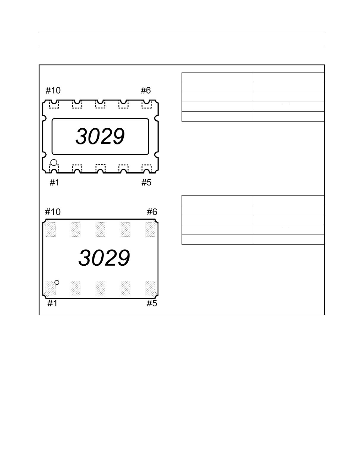
9.2. MARKING AND PIN #1 INDEX ................................................................................................................ 61
10. PACKING INFORAMTION ............................................................................................................................... 62
10.1. CARRIER TAPE ....................................................................................................................................... 62
10.2. PARTS PER REEL ................................................................................................................................... 63
10.3. REEL 13 INCH FOR 12 mm TAPE .......................................................................................................... 64
10.4. REEL 7 INCH FOR 12 mm TAPE ............................................................................................................ 65
11. HANDLING PRECAUTIONS FOR CRYSTALS OR MODULES WITH EMBEDDED CRYSTALS ................ 66
12. DOCUMENT REVISION HISTORY .................................................................................................................. 67
4/67

Micro Crystal
DTCXO Temperature Compensated Real Time Clock / Calendar Module RV-3029
RV-3029
Highly accurate, DTCXO Temperature Compensated Real Time Clock / Calendar Module
with I2C Interface
1. OVERVIEW
• RTC module with built-in “Tuning Fork” crystal oscillating at 32.768 kHz
• Factory calibrated, all built-in Temperature Compensation circuitry
Time accuracy: Temperature Range Opt: A Opt: B
25°C +/- 3 ppm +/- 3 ppm
0°C to + 50°C +/- 4 ppm +/- 5 ppm
-10°C to + 60°C +/- 5 ppm +/- 10 ppm
-40°C to + 85°C +/- 6 ppm +/- 25 ppm
• Ultra low power consumption: 800nA typ @ VDD = 3.0V / T
• Wide clock operating voltage: 1.3 – 5.5V
• Wide interface operating voltage: 1.4 – 5.5V
• Extended operating temperature range: -40°C to +125°C
• I2C serial interface with fast mode SCL clock frequency of 400 kHz
• Provides year, month, day, weekday, hours, minutes and seconds
• Highly versatile alarm and timer functions
• Integrated Low-Voltage Detector, Power-On Reset and Self-Recovery System
• Main Power Supply to Backup Battery switchover circuitry with Trickle Charger
• Programmable CLKOUT pins for peripheral devices (32.768 kHz / 1024 Hz / 32 Hz / 1 Hz)
• Available in 2 different small and compact package sizes, RoHS-compliant and 100% leadfree:
C2: 5.0 x 3.2 x 1.2 mm
C3: 3.7 x 2.5 x 0.9 mm
1.1. GENERAL DESCRIPTION
The RV-3029 is a CMOS low power, real-time clock/calendar module with built-in Thermometer and Digital
Temperature Compensation circuitry (DTCXO). The temperature compensation circuitry is factory-calibrated and
greatly improves the time accuracy by compensating the frequency-deviation @ 25°C and the anticipated
frequency-drift over the temperature of the embedded 32.768 kHz “Tuning-Fork” crystal, even over the extended
Temperature Range -40°C to +125°C. Data is transferred serially via an I2C interface with a maximum SCL clock
frequency in fast mode of 400 kHz, the built-in word address register is incremented automatically after each
written or read data byte. Beyond standard RTC-functions like year, month, day, weekday, hours, minutes, seconds
information, the RV-3029 offers highly versatile Alarm and Timer-Interrupt function, programmable Clock-Output
and Low-Voltage Detector.
1.2. APPLICATIONS
The RV-3029 RTC module combines key functions with outstanding performance in a small ceramic package:
• Factory calibrated Temperature Compensation
• Extended temperature range up to +125°C
• Low Power consumption
• Smallest temperature compensated RTC module with embedded Xtal
These unique features make this product perfectly suitable for many applications:
• Automotive: Car Radio / GPS and Tracking Systems / Dashboard / Engine Controller /
Car Mobile & Entertainment Systems / Tachometers
• Metering: E-meter / Heating Counter
• Outdoor: ATM & POS systems / Surveillance & Safety systems / Ticketing systems
• All kind of portable and battery operated devices
• Industrial and consumer electronics
• White goods
5/67
-40°C to +125°C +/- 8 ppm +/- 30 ppm
amb
= 25°C

Micro Crystal
DTCXO Temperature Compensated Real Time Clock / Calendar Module RV-3029
2. BLOCK DIAGRAM
CLKOUT
CLKOE
INT
V
DD
V
BACKUP
V
SS
SCL
SDA
32.768 kHz
Xtal
OSC
OUTPUT
CONTROL
I2C-BUS
2-wire
Serial
Interface
POWER
CONTROL
DIVIDER
and
TEMPERATURE
COMPENSATION
LOGIC
SYSTEM
CONTROL
LOGIC
TEMPERATURE
SENSOR
Control_1
Control_INT
Control_INT-Flags
Control_Status
Control_Reset
Seconds
Minutes
Hours
Date
Weekday
Month
Year
Seconds Alarm
Minutes Alarm
Hour Alarm
Day Alarm
Weekday Alarm
Month Alarm
Year Alarm
Timer Low
Timer High
Temperature °K
User EEPROM
2 Bytes
EE Ctrl
Xtal Deviation
Xtal Temp-Coef
Xtal T0 Temp
User RAM
8 Byte
User RAM
00
08
10
18
20
28
29
30
38
3F
6/67
Micro Crystal
INT
INT
DTCXO Temperature Compensated Real Time Clock / Calendar Module RV-3029
2.1. PINOUT
C2 Package:
C3 Package:
#1 VDD #10 CLKOE
#2 CLKOUT #9 N.C.
#3 N.C.
#4 SCL
#8 V
#7
BACKUP
#5 SDA #6 VSS
#1 CLKOE #10 N.C.
#2 VDD #9 V
BACKUP
#3 CLKOUT #8 N.C.
#4 SCL
#7
#5 SDA #6 VSS
7/67
Micro Crystal
DTCXO Temperature Compensated Real Time Clock / Calendar Module RV-3029
2.2. PIN DESCRIPTION
Symbol
VDD 1 2
CLKOUT 2 3
N.C. 3 8 Not Connected; internally used for test, do not connect other signals then ground
SCL 4 4 Serial Clock Input pin; requires pull-up resistor
SDA 5 5 Serial Data Input-Output pin; open-drain; requires pull-up resistor
VSS 6 6 Ground
INT
V
8 9 Backup Supply Voltage; tie to GND when not using backup supply voltage
BACKUP
N.C. 9 10 Not Connected; internally used for test, do not connect other signals then ground
CLKOE 10 1 CLKOUT enable/disable pin; enable is active HIGH; tie to GND when not using CLKOUT
Pin #
C2 C3
7 7 Interrupt Output pin; open-drain; active LOW
Description
Positive supply voltage; positive or negative steps in supply voltage may affect oscillator
performance, recommend 10 nF decoupling capacitor close to device
Clock Output pin; CLKOUT or
CLKOUT output push-pull /
function can be selected.(Control_1; bit7; Clk/Int)
INT
INT function open-drain requiring pull-up resistor
2.3. FUNCTIONAL DESCRIPTION
The RV-3029 is a highly accurate real-time clock/calendar module due to integrated temperature compensation
circuitry. The built-in Thermometer and Digital Temperature Compensation circuitry (DTCXO) provides improved
time-accuracy; achieved by measuring the temperature and calculating an expected correction value based on
precise, factory-calibrated Crystal parameters. The compensation of the frequency deviation @ 25°C and the
Crystal’s frequency-drift over the temperature range are obtained by adding or subtracting 32.768 kHz oscillator
clock-pulses. Beyond standard RTC-functions like year, month, day, weekday, hours, minutes, seconds
information, the RV-3029 offers highly versatile Alarm and Timer-Interrupt function, programmable Clock-Output
and Voltage-Low-Detector and a Main-Supply to Backup-Battery Switchover Circuitry and a 400 kHz I2C interface.
The CMOS IC contains thirty 8-bit RAM registers organized in 6 memory pages; the address counter is
automatically incremented within the same memory page. All sixteen registers are designed as addressable 8-bit
parallel registers, although, not all bits are implemented.
• Memory page #00 contains of five registers (memory address 00h and 04h) used as control registers
• Memory page #01 addresses 08h through 0Eh are used as counters for the clock function (seconds up to
years). The Seconds, Minutes, Hours, Days, Weekdays, Months and Years registers
are all coded in Binary-Coded-Decimal (BCD) format. When one of the RTC registers is
read, the content of all counters is frozen to prevent faulty reading of the clock/calendar
registers during a carry condition
• Memory page #02 addresses 10h through 16h define the alarm condition
• Memory page #03 addresses 18h and 19h are used for Timer function
• Memory page #04 address 20h provides the thermometer reading value
• Memory page #07 addresses 38h through 3Fh are available for user data
Additionally, the CMOS-IC contains six non-volatile 8-bit EEPROM registers organized in 2 memory pages; the
address counter is automatically incremented within the same memory page.
• EEPROM page #05 addresses 28h and 29h are available for EEPROM user data
• EEPROM page #06 contains of four registers (memory address 30h through 33h) used as non-volatile
control registers. These registers contain the factory programmed parameters of the
Crystal’s thermal characteristics, the frequency-deviation @ ambient temperature and
the Thermometer’s calibration values. In favour for the best time-accuracy, the factory
programmed registers (memory address 31h through 33h) shall not be changed by
the user without carefully studying its function
8/67

Micro Crystal
DTCXO Temperature Compensated Real Time Clock / Calendar Module RV-3029
2.4. DEVICE PROTECTION DIAGRAM
9/67

Micro Crystal
Control page
Timer page
Temperature page
EEPROM
User
EEPROM Control page
RAM page
DTCXO Temperature Compensated Real Time Clock / Calendar Module RV-3029
3. REGISTER ORGANIZATION
The registers are grouped into memory pages. The pages are addressed by the 5 most-significant-bits (MSB’s bits
7 – 3), the 3 least-significant-bites (LSB’s 2 – 0) select the registers within the addressed page.
30 RAM registers organized in 6 memory pages and 6 EEPROM registers organized in 2 memory pages are
available. During interface access, the page address (MSB’s 7 - 3) is fixed while the register address (LSB’s 2 - 0)
are automatically incremented. The content of all counters and registers are frozen to prevent faulty reading of the
clock/calendar registers during carry condition.
The time registers in the Clock and Alarm pages are encoded in the Binary Coded Decimal format (BCD) to simplify
application use. Other registers are either bit-wise or standard binary format.
3.1. REGISTER OVERVIEW
Address
Page Address
Bit 7 - 3 Bit 2 - 0
000 00h Control_1
001 01h Control_INT
010 02h Control_INT Flag
011 03h Control_Status
100 04h Control_Reset
000
001
010
011
100
101
110
000
001
010
011
100
101
110
00000
Clock page
00001
Alarm page
00010
000
00011
00100
001
000 20h Temperature
000
00101
001
000
00110
001
010
011
000
00111
:
111
Bit positions labelled as “X” are not implemented and will return a “0” when read.
Function Bit 7 Bit 6 Bit 5 Bit 4 Bit 3 Bit 2 Bit 1 Bit 0
Hex
Clk/Int TD1 TD0 SROn EERE TAR TE WE
X X X SRIE V2IE V1IE TIE AIE
X X X SRF V2IF V1IF TF AF
EEbusy X PON SR V2F V1F X X
X X X SysR X X X X
08h Seconds
09h Minutes
0Ah Hours
0Bh Days
0Ch Weekdays
0Dh Months
0Eh Years
10h Second Alarm
11h Minute Alarm
12h Hour Alarm
13h Days Alarm
14h Weekday Alarm
15h Months Alarm
16h Year Alarm
18h Timer Low
19h Timer High
28h EEPROM User
29h EEPROM User
30h EEPROM Contr.
31h Xtal Offset
32h Xtal Coef
33h Xtal T0
X 40 20 10 8 4 2 1
X 40 20 10 8 4 2 1
X 12-24 20-PM 10 8 4 2 1
X X 20 10 8 4 2 1
X X X X X 4 2 1
X X X 10 8 4 2 1
X 40 20 10 8 4 2 1
AE_S 40 20 10 8 4 2 1
AE_M 40 20 10 8 4 2 1
AE_H X 20-PM 10 8 4 2 1
AE_D X 20 10 8 4 2 1
AE_W X X X X 4 2 1
AE_M X X 10 8 4 2 1
AE_Y 40 20 10 8 4 2 1
128 64 32 16 8 4 2 1
128 64 32 16 8 4 2 1
128 64 32 16 8 4 2 1
2 bytes of EEPROM for user data
R80k R20k R5k R1k FD1 FD0 ThE ThP
sign 64 32 16 8 4 2 1
128 64 32 16 8 4 2 1
X X 32 16 8 4 2 1
38h
:
User RAM
8 bytes of RAM for user data
3Fh
10/67
Micro Crystal
DTCXO Temperature Compensated Real Time Clock / Calendar Module RV-3029
3.2. CONTROL PAGE REGISTER FUNCTION
3.2.1. CONTROL_1 (address 00h…bits description)
Address Function Bit 7 Bit 6 Bit 5 Bit 4 Bit 3 Bit 2 Bit 1 Bit 0
00h Control_1 Clk/Int TD1 TD0 SROn EERE TAR TE WE
Bit Symbol Value Description Reference
0
7 Clk/Int
6 TD1
5 TD0
4 SROn
3 EERE
2 TAR
1 TE
0 WE
3.2.2. CONTROL_INT (address 01h…bits description)
Applies INT function on CLKOUT pin
1 Applies CLKOUT function on CLKOUT pin
00
01
Select Source Clock for internal Countdown Timer See section 4.4.
10
11
0 Disables Self Recovery function
1 Enables Self Recovery function
0 Disables automatic EEPROM refresh every hour
1 Enables automatic EEPROM refresh every hour
0 Disables Countdown Timer auto-reload mode
1 Enables Countdown Timer auto-reload mode
0 Disables Countdown Timer
1 Enables Countdown Timer
0 Disables 1Hz Clock Source for Watch
1 Enables 1Hz Clock Source for Watch
See section 4.9.
See section 4.8.
See section 4.3.
See section 4.4.
See section 4.4.
See section 4.7.
Address Function Bit 7 Bit 6 Bit 5 Bit 4 Bit 3 Bit 2 Bit 1 Bit 0
01h Control_INT X X X SRIE V2IE V1IE TIE AIE
Bit Symbol Value Description Reference
7 to 5 unused X Unused
4 SRIE
3 V2IE
2 V1IE
1 TIE
0 AIE
0 Disables Self-Recovery INT
1 Enables Self-Recovery INT
0 Disables VLOW2 INT; “Low Voltage 2 detection”
1 Enables VLOW2 INT; “Low Voltage 2 detection”
0 Disables VLOW1 INT; “Low Voltage 1detection”
1 Enables VLOW1 INT; “Low Voltage 1detection”
0 Disables Countdown Timer INT
1 Enables Countdown Timer INT
0 Disables Alarm INT
1 Enables Alarm INT
See section 4.8.
See section 4.1.2.
See section 4.1.2.
See section 4.4.1.
See section 4.5.1.
Bit positions labelled as “X” are not implemented and will return a “0” when read.
11/67

Micro Crystal
DTCXO Temperature Compensated Real Time Clock / Calendar Module RV-3029
3.2.3. CONTROL_INT FLAG (address 02h…bits description)
Address Function Bit 7 Bit 6 Bit 5 Bit 4 Bit 3 Bit 2 Bit 1 Bit 0
02h Control_INT Flag X X X SRF V2IF V1IF TF AF
Bit Symbol Value Description Reference
7 to 5 unused X Unused
0 No Self-Recovery Interrupt generated
4 SRF
Self-Recovery Interrupt generated if possible
1
deadlock is detected; clear flag to clear Interrupt
See section 4.6.
0 No VLOW2 Interrupt generated
3 V2IF
VLOW2 Interrupt generated when supply voltage
1
drops below VLOW2 threshold
See section 4.6.
0 No VLOW1 Interrupt generated
2 V1IF
VLOW1 Interrupt generated when supply voltage
1
drops below VLOW1 threshold
See section 4.6.
0 No Timer Interrupt generated
1 TF
Timer Interrupt generated when Countdown Timer
1
value reaches zero
See section 4.6.
0 No Alarm Interrupt generated
0 AF
Alarm Interrupt generated when Time & Date
1
matches Alarm setting
See section 4.6.
Bit positions labelled as “X” are not implemented and will return a “0” when read.
3.2.4. CONTROL_STATUS (address 03h…bits description)
Address Function Bit 7 Bit 6 Bit 5 Bit 4 Bit 3 Bit 2 Bit 1 Bit 0
03h Control_Status EEbusy X PON SR V2F V1F X X
Bit Symbol Value Description Reference
0 EEPROM is not busy
7 EEbusy
Flag is set when EEPROM page is busy due to
1
“write” or automatic EEPROM refresh in progress
6 unused X Unused
See section 4.3.
0 No Power-On Reset executed
5 PON
4 SR
Flag is set at Power-On, flag must be cleared by
1
writing “0”
No Self-Recovery Reset or System Reset has
0
been generated.
Flag is set when Self-Recovery Reset or System
1
Reset has been generated.
See section 4.1.
See section 4.2.1.
0 No VLOW2 Interrupt generated”
3 V2F
VLOW2 Interrupt generated when supply voltage
1
drops below VLOW1 threshold
See section 4.6.
0 No VLOW1 Interrupt generated”
2 V1F
VLOW1 Interrupt generated when supply voltage
1
drops below VLOW1 threshold
1 to 0 unused X Unused
See section 4.6.
Bit positions labelled as “X” are not implemented and will return a “0” when read.
12/67

Micro Crystal
1
)
DTCXO Temperature Compensated Real Time Clock / Calendar Module RV-3029
3.2.5. CONTROL_RESET (address 04h…bits description)
Address Function Bit 7 Bit 6 Bit 5 Bit 4 Bit 3 Bit 2 Bit 1 Bit 0
04h Control_Reset X X X SysR X X X X
Bit Symbol Value Description Reference
7 to 5 unused X Unused
0 No System Reset will be executed
4 SysR
3 to 0 unused X Unused
Bit positions labelled as “X” are not implemented and will return a “0” when read.
Set bit = “1” triggers a System Reset. After the
1
restart of the logic, the SysR will be cleared and in
bit 4 “SR” in the register Control_Status will be set
See section 4.2.1.
3.3. WATCH PAGE REGISTER FUNCTION
Watch Page registers are coded in the Binary Coded Decimal (BCD) format; BCD format is used to simplify
application use.
3.3.1. SECONDS, MINUTES, HOURS, DAYS, WEEKDAYS, MONTHS, YEARS REGISTER
Seconds (address 08h…bits description)
Address Function Bit 7 Bit 6 Bit 5 Bit 4 Bit 3 Bit 2 Bit 1 Bit 0
08h Seconds X 40 20 10 8 4 2 1
Bit Symbol Value Description
7 X - Unused
6 to 0 Seconds 0 to 59 This register holds the current seconds coded in BCD format
Minutes (address 09h…bits description)
Address Function Bit 7 Bit 6 Bit 5 Bit 4 Bit 3 Bit 2 Bit 1 Bit 0
09h Minutes X 40 20 10 8 4 2 1
Bit Symbol Value Description
7 X - Unused
6 to 0 Minutes 0 to 59 This register holds the current minutes coded in BCD format
Hours (address 0Ah…bits description)
Address Function Bit 7 Bit 6 Bit 5 Bit 4 Bit 3 Bit 2 Bit 1 Bit 0
0Ah Hours X 12-24
20-PM
10 8 4 2 1
Bit Symbol Value Description
7 X - Unused
12 hour mode (AM/PM)
6 12-24
5 20-PM
4 to 0 Hours
24 hour mode
1)
User is requested to pay attention setting valid data only.
13/67
6 12-24
5 to 0 Hours1) 0 to 23 This register holds the current hours coded in BCD format
0 Selects 24-hour mode
1 Selects 12-hour (AM/PM) mode
0 Indicates AM
1 Indicates PM
1 to 12 This register holds the current hours coded in BCD format
0 Selects 24-hour mode
1 Selects 12-hour AM/PM mode

Micro Crystal
1
)
DTCXO Temperature Compensated Real Time Clock / Calendar Module RV-3029
Days (address 0Bh…bits description)
Address Function Bit 7 Bit 6 Bit 5 Bit 4 Bit 3 Bit 2 Bit 1 Bit 0
0Bh Days X X 20 10 8 4 2 1
Bit Symbol Value Description
7 to 6 X - Unused
5 to 0 Days 1 to 31
1)
The RTC compensates for leap years by adding a 29th day to February if the year counter contains a value which is exactly divisible by 4;
including the year 00.
This register holds the current days coded in BCD format 1)
Weekdays (address 0Ch…bits description)
Address Function Bit 7 Bit 6 Bit 5 Bit 4 Bit 3 Bit 2 Bit 1 Bit 0
0Ch Weekdays X X X X X 4 2 1
Bit Symbol Value Description
7 to 3 X - Unused
2 to 0 Weekdays 1 to 7
Weekdays
Bit 7 Bit 6 Bit 5 Bit 4 Bit 3 Bit 2 Bit 1 Bit 0
This register holds the current weekdays coded in BCD format 1)
Sunday X X X X X 0 0 1
Monday X X X X X 0 1 0
Tuesday X X X X X 0 1 1
Wednesday X X X X X 1 0 0
Thursday X X X X X 1 0 1
Friday X X X X X 1 1 0
Saturday X X X X X 1 1 1
1)
These bits may be re-assigned by the user.
Months (address 0Dh…bits description)
Address Function Bit 7 Bit 6 Bit 5 Bit 4 Bit 3 Bit 2 Bit 1 Bit 0
0Dh Months X X X 10 8 4 2 1
Bit Symbol Value Description
7 to 5 X - Unused
4 to 0 Months 1 to 12
Months Bit 7 Bit 6 Bit 5 Bit 4 Bit 3 Bit 2 Bit 1 Bit 0
January X X X 0 0 0 0 1
February X X X 0 0 0 1 0
March X X X 0 0 0 1 1
April X X X 0 0 1 0 0
May X X X 0 0 1 0 1
June X X X 0 0 1 1 0
July X X X 0 0 1 1 1
August X X X 0 1 0 0 0
September X X X 0 1 0 0 1
October X X X 1 0 0 0 0
November X X X 1 0 0 0 1
December X X X 1 0 0 1 0
1)
The RTC compensates for leap years by adding a 29th day to February if the year counter contains a value which is exactly divisible by 4;
including the year 00.
This register holds the current months coded in BCD format 1)
14/67
Micro Crystal
DTCXO Temperature Compensated Real Time Clock / Calendar Module RV-3029
Years (address 0Eh…bits description)
Address Function Bit 7 Bit 6 Bit 5 Bit 4 Bit 3 Bit 2 Bit 1 Bit 0
0Eh Years X 40 20 10 8 4 2 1
Bit Symbol Value Description
7 X - Unused
6 to 0 Years 0 to 79
1)
The RTC compensates for leap years by adding a 29th day to February if the year counter contains a value which is exactly divisible by 4;
including the year 00.
This register holds the current year 20xx coded in BCD format1)
3.3.2. DATA FLOW OF TIME AND DATE FUNCTION
1 Hz tick
SECONDS
MINUTES
12_24 hour mode
LEAP YEAR
CALCULATION
HOURS
DAYS
MONTHS
YEARS
WEEKDAY
15/67

Micro Crystal
INT
DTCXO Temperature Compensated Real Time Clock / Calendar Module RV-3029
3.4. ALARM PAGE REGISTER FUNCTION
The Alarm Page registers contain alarm information. When one or more of these registers are loaded with a valid
second, minute, hour, day, weekday, month or year information and its corresponding alarm enable bit (AE_x) is
logic “1”, then that information will be compared with the current time / date information in the Watch Page
registers.
When all enabled comparisons first match (wired “AND”) and the AIE Flag (bit 0 in register Control_INT) is enabled,
then the AF Flag (bit 0 in register Control_INT) is set = “1” and an Interrupt signal becomes available at
Disabled Alarm registers which have their corresponding bit AE_X at logic “0” are ignored.
3.4.1. SECONDS, MINUTES, HOURS, DAYS, WEEKDAYS, MONTHS, YEARS ALARM REGISTER
Alarm Seconds (address 10h…bits description)
Address Function Bit 7 Bit 6 Bit 5 Bit 4 Bit 3 Bit 2 Bit 1 Bit 0
10h Second Alarm AE_S 40 20 10 8 4 2 1
Bit Symbol Value Description
7 AE_S
6 to 0 Seconds Alarm 0 to 59 These bits hold the Second Alarm information coded in BCD format
0 Second Alarm is disabled
1 Second Alarm is enabled
Alarm Minutes (address 11h…bits description)
Address Function Bit 7 Bit 6 Bit 5 Bit 4 Bit 3 Bit 2 Bit 1 Bit 0
11h Minute Alarm AE_M 40 20 10 8 4 2 1
Bit Symbol Value Description
7 AE_M
6 to 0 Minutes Alarm 0 to 59 These bits hold the Minute Alarm information coded in BCD format
0 Minute Alarm is disabled
1 Minute Alarm is enabled
Alarm Hours (address 12h…bits description)
Address Function Bit 7 Bit 6 Bit 5 Bit 4 Bit 3 Bit 2 Bit 1 Bit 0
12h Hours Alarm AE_H 12-24 20-PM 10 8 4 2 1
pin.
Bit Symbol Value Description
7 AE_H
6 X - Unused
12 hour mode (AM/PM)
5 20-PM
4 to 0 Hours Alarm 1 to 12
24 hour mode
16/67
5 to 0 Hours Alarm 0 to 23
0 Hour Alarm is disabled
1 Hour Alarm is enabled
0 Indicates AM
1 Indicates PM
These registers hold the Hours Alarm information coded in BCD format
when in 12 hour mode
These registers hold the Hours Alarm information coded in BCD format
when in 24 hour mode

Micro Crystal
DTCXO Temperature Compensated Real Time Clock / Calendar Module RV-3029
Alarm Days (address 13h…bits description)
Address Function Bit 7 Bit 6 Bit 5 Bit 4 Bit 3 Bit 2 Bit 1 Bit 0
13h Days Alarm AE_D X 20 10 8 4 2 1
Bit Symbol Value Description
7 AE_D
6 X - Unused
5 to 0 Days Alarm 1 to 31 These registers hold the Day Alarm information coded in BCD
0 Day Alarm is disabled
1 Day Alarm is enabled
Alarm Weekdays (address 14h…bits description)
Address Function Bit 7 Bit 6 Bit 5 Bit 4 Bit 3 Bit 2 Bit 1 Bit 0
14h Weekday Alarm AE_W X X X X 4 2 1
Bit Symbol Value Description
7 AE_W
6 to 3 X - Unused
2 to 0 Weekday Alarm 1 to 7 These registers hold the Weekday Alarm information coded in BCD
0 Weekday Alarm is disabled
1 Weekday Alarm is enabled
Alarm Months (address 15h…bits description)
Address Function Bit 7 Bit 6 Bit 5 Bit 4 Bit 3 Bit 2 Bit 1 Bit 0
15h Months Alarm AE_M X X 10 8 4 2 1
Bit Symbol Value Description
7 AE_W
6 to 5 X - Unused
4 to 0 Months Alarm 1 to 12 These registers hold the Months Alarm information coded in BCD
0 Months Alarm is disabled
1 Months Alarm is enabled
Alarm Years (address 16h…bits description)
Address Function Bit 7 Bit 6 Bit 5 Bit 4 Bit 3 Bit 2 Bit 1 Bit 0
16h Year Alarm AE_Y 40 20 10 8 4 2 1
Bit Symbol Value Description
7 AE_Y
6 to 0 Year Alarm 0 to 79 These registers hold the Year Alarm information coded in BCD
17/67
0 Year Alarm is disabled
1 Year Alarm is enabled

Micro Crystal
DTCXO Temperature Compensated Real Time Clock / Calendar Module RV-3029
3.5. TIMER PAGE REGISTER FUNCTION
The Timer Page contains 2 registers forming a 16-bit count down timer value.
Countdown Timer Value (addresses 18h / 19h…bits description)
Address Function Bit 7 Bit 6 Bit 5 Bit 4 Bit 3 Bit 2 Bit 1 Bit 0
18h Timer Low 128 64 32 16 8 4 2 1
19h Timer High 128 64 32 16 8 4 2 1
Address Symbol Value Description
18h Timer Low
19h Timer High
1 to 255
0 to 255
These bits hold the Low Countdown Timer Value in binary format
These bits hold the High Countdown Timer Value in binary format
3.6. TEMPERATURE PAGE REGISTER FUNCTION
The Temperature Page register contains the result of the measured temperature ranging from -60°C (=0d) to
+190°C (=250d) with 0°C corresponding to a content of =60d.
During read / write access, the content of the register Temperature is frozen in a cache memory to prevent faulty
reading.
When the Thermometer is disabled by ThE = “0” (bit 1 in register EEPROM_Control), the register Temperature at
address 20h can be externally written.
Temperature Value (address 20h…bits description)
Address Function Bit 7 Bit 6 Bit 5 Bit 4 Bit 3 Bit 2 Bit 1 Bit 0
20h Temperature 128 64 32 16 8 4 2 1
Address Symbol Value Description
20h Temperature
-60 to
+194°C
These bits hold the Temperature Value coded in binary format
3.7. EEPROM DATA PAGE REGISTER FUNCTION
The EEPROM Data Page contains 2 non-volatile EEPROM registers for user’s application.
Please see section 4.3 EEPROM MEMORX ACCESS for detailed instructions how to handle EEPROM read / write
access.
User EEPROM Data Registers (addresses 28h / 29h…bits description)
Address Function Bit 7 Bit 6 Bit 5 Bit 4 Bit 3 Bit 2 Bit 1 Bit 0
28h EEPROM User 128 64 32 16 8 4 2 1
29h EEPROM User 128 64 32 16 8 4 2 1
Address Symbol Value Description
28h EEPROM User
29h EEPROM User
0 to 255
0 to 255
EEPROM User Data (2 Bytes)
18/67

Micro Crystal
DTCXO Temperature Compensated Real Time Clock / Calendar Module RV-3029
3.8. EEPROM CONTROL PAGE REGISTER FUNCTION
The EEPROM Control Page contains 4 non-volatile EEPROM registers.
With Register EEPROM Control, the settings for Trickle-Charger (bit 7-4), the CLKOUT frequency (bit 3&2) and the
Thermometer (bit 1&0) can be controlled.
The registers XTAL Offset, XTAL Coef and XTAL T0 contain the factory calibrated, individual crystal parameters to
compensate the frequency deviation over the temperature range.
Please see section 4.3 EEPROM MEMORY ACCESS for detailed instructions how to handle EEPROM read / write
access.
3.8.1. EEPROM CONTROL (address 30h…bits description)
Address Function Bit 7 Bit 6 Bit 5 Bit 4 Bit 3 Bit 2 Bit 1 Bit 0
30h EEPROM Control R80k R20k R5k R1k FD1 FD0 ThE ThP
Bit Symbol Value Description Reference
7 R80k
6 R20k
5 R5k
4 R1k
3 FD1
2 FD0
1 ThE
0 ThP
3.8.2. XTAL OFFSET (address 31h…bits description)
0 Disables 80 kΏ trickle charge resistor
1 Enables 80 kΏ trickle charge resistor
0 Disables 20 kΏ trickle charge resistor
1 Enables 20 kΏ trickle charge resistor
0 Disables 5 kΏ trickle charge resistor
1 Enables 5 kΏ trickle charge resistor
0 Disables 1.5 kΏ trickle charge resistor
1 Enables 1.5 kΏ trickle charge resistor
00
01
Selects Clock Frequency at CLKOUT pin See section 4.9.
10
11
0 Disables Thermometer
1 Enables Thermometer
0 Set Temperature Scanning Interval: 1 second
1 Set Temperature Scanning Interval: 16 seconds
See section 4.1.
See section 5.2.1.
See section 5.2.1.
Address Function Bit 7 Bit 6 Bit 5 Bit 4 Bit 3 Bit 2 Bit 1 Bit 0
31h XTAL Offset sign 64 32 16 8 4 2 1
Bit Symbol Value Description Reference
7 Sign
6 to 0 XTAL Offset1)
1)
The XTAL Offset register value is factory programmed according to the crystal’s initial frequency-tolerance. For best time-accuracy, the
content of this register must not be changed by the user.
0 - Deviation (slower) of 32.768kHz frequency at T0
1 + Deviation (faster) of 32.768kHz frequency at T0
0 to 121
Frequency Offset Compensation value
See section 5.2.2.
3.8.3. XTAL TEMPERATUR COEFFICIENT (address 32h…bits description)
Address Function Bit 7 Bit 6 Bit 5 Bit 4 Bit 3 Bit 2 Bit 1 Bit 0
32h XTAL Coef
Bit Symbol Value Description Reference
7 to 0 XTAL Coef1)
1)
The XTAL Coef register value is factory programmed according to the crystal parameters over temperature. For best time-accuracy, the
content of this register must not be changed by the user.
19/67
128 64 32 16 8 4 2 1
0 to 255
Quadratic Coefficient of XTAL’s Temperature Drift See section 5.2.2.

Micro Crystal
DTCXO Temperature Compensated Real Time Clock / Calendar Module RV-3029
3.8.4. XTAL TURNOVER TEMPERATUR COEFFICIENT T0 (address 33h…bits description)
Address Function Bit 7 Bit 6 Bit 5 Bit 4 Bit 3 Bit 2 Bit 1 Bit 0
33h XTAL T0
x x 32 16 8 4 2 1
Bit Symbol Value Description Reference
7 to 6 x - Unused
5 to 0 XTAL T01) 4 to 67 XTAL’s Turnover Temperature in °C See section 5.2.2.
1)
The XTAL T0 register value is factory programmed according to the crystal parameters over temperature. For best time-accuracy, the
content of this register must not be changed by the user.
3.9. RAM DATA PAGE REGISTER FUNCTION
The RAM Data Page contains 8 RAM registers for user’s application.
User RAM Data Registers (addresses 38h to 3Fh…bits description)
Address Function Bit 7 Bit 6 Bit 5 Bit 4 Bit 3 Bit 2 Bit 1 Bit 0
38h RAM User
--- ---
3Fh RAM User
Address Symbol Value Description
38h RAM User
--- --- ---
3Fh RAM User
128 64 32 16 8 4 2 1
128 64 32 16 8 4 2 1
128 64 32 16 8 4 2 1
0 to 255
RAM User Data (8 Bytes)
0 to 255
20/67

Micro Crystal
INT
INT
DTCXO Temperature Compensated Real Time Clock / Calendar Module RV-3029
4. DETAILED FUNCTIONAL DESCRIPTION
4.1. POWER-UP, POWER MANAGEMENT AND BATTERY SWITCHOVER
The RV-3029 has two power supply pins:
• VDD the main power supply input pin
• V
BACKUP
The RV-3029 has multiple power management function implemented:
• Automatic switchover function between main power supply and backup supply voltage. The higher supply
voltage is selected automatically, with a switchover hysteresis of 20mV
• Low supply voltage detection V
control bits are enabled
• Functions requiring a minimum supply voltage are automatically disabled if low supply voltage is detected
• Interface and CLKOUT are automatically disabled when the device operates in backup supply mode
• Programmable trickle charge circuitry to charge backup battery or supercap
Backup Switchover Circuitry Disables non-used Functions
the backup battery input pin
and V
LOW1
with the possibility to generate an
LOW2
if the corresponding
1
Trickle charge circuitry is enabled by software when selecting trickle-charge resistors. When back-up
supply switchover-circuitry switches to the backup supply voltage, trickle charge function is disabled.
2
The implemented backup switchover circuitry continuously compares VDD and V
connects the higher of them to the internal supply voltage V
The switchover hysteresis from VDD to V
3
When the device is operating at the V
BACKUP
and vice versa is typically 20mV.
BACKUP
supply voltage, non-used RTC functions are disabled to
INT
.
voltages and
BACKUP
ensure optimized power consumption:
• I2C interface Disabled when operating in V
• CLKOUT Disabled when operating in V
•
Enabled even when operating in V
• Trickle Charge Disabled when operating in V
21/67
BACKUP
BACKUP
BACKUP
mode
mode
BACKUP
mode
mode

Micro Crystal
DTCXO Temperature Compensated Real Time Clock / Calendar Module RV-3029
4.1.1. POWER UP SEQUENCE
The device can be either powered up from main supply VDD or from backup supply V
BACKUP
.
During power-up, the chip is executing the following power-up procedure:
• The implemented battery switchover circuitry compares VDD and V
voltages and connects the higher
BACKUP
of them to supply the chip
• At power-up, the chip is kept in Reset state until the supply voltage reaches an internal threshold level.
Once the supply voltage is higher than this threshold level, a Reset is executed and registers are loaded
with the Register Reset Values described in section 4.2.2. REGISTER RESET VALUES
• After the Reset is executed and registers are loaded with the Register Reset Values, “PON” is set = “1” (bit
5 in Register Control-Status), it needs to be cleared by writing = “0”
• Once the supply voltage reaches the oscillator start-up voltage, the oscillator-circuitry starts the 32.768 kHz
“tuning-fork” Crystal typically within 500 ms
• Once the 32.768 kHz clocks are present, the Voltage Detector starts in fast mode to monitor the supply
voltage, the accelerated scanning of the supply voltage will slightly increase the current consumption.
• When a supply voltage >V
is detected, the fast mode voltage detection is stopped, and the EEPROM
Low2
read is enabled
• Configuration registers are loaded with the configuration data read from the EEPROM Control Page and
the bits V
Low1
and V
are reset = “0”
Low2
• If the Thermometer is enabled by “ThE” = “1” (bit 1 in register EEPROM_Control), the temperature is
measured and the frequency compensation value for time correction is calculated
• The RV-3029 becomes fully functional; the correct Time / Date information needs to be loaded into the
corresponding registers and bit 5 “PON” in Register Control-Status needs to be cleared by writing “0”
Note 1:
During power up, the Low Voltage Detection is monitoring the supply voltage at an accelerated scan rate
increasing the current consumption of the device.
Once power supply voltage exceed V
threshold, the flags V
LOW2
LOW1
and V
are cleared and the scan rate for
LOW2
the low voltage detection is set to 1 second to ensure optimized power consumption.
Note 2:
Please not the different meaning of the “PON”; “V
Low1
” and “V
Low2
” Flags:
PON
“PON” Flag is set after Power-Up Reset is executed
• Indicating that time & date information are corrupted
V
Low1
V
Flag is set when supply voltage drops below V
Low1
threshold
Low1
• Indicating that the Thermometer might have been disabled due to low supply voltage and the temperature
compensation was operating for a while with the last temperature reading causing bigger time-deviation
V
Low2
V
Flag is set when supply voltage drops below V
Low1
threshold
Low2
• Indicating a risk that the 32.768kHz might have stopped due to low supply voltage and that the time & date
information might be corrupted
22/67

Micro Crystal
DTCXO Temperature Compensated Real Time Clock / Calendar Module RV-3029
Example Power Up sequence, Low Voltage detection and Backup Supply switchover
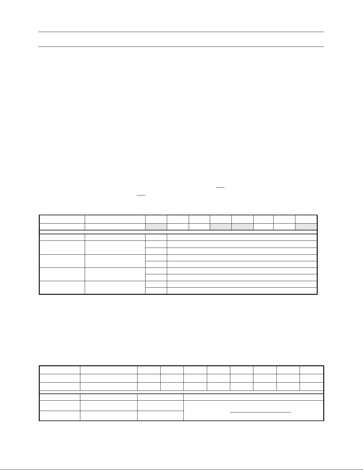
1
Power Up Reset is executed; registers are loaded with Reset Values. PON flag is set at Power up
indicating that time / date information likely are corrupted.
Low voltage detection flags V
2
PON Flag needs to be cleared by software writing “0”.
3
Trickle charge circuitry for backup battery can be enabled by software.
4
Switchover to the backup supply voltage when VDD drops below VDD < (V
5
Low voltage detection sets V
6
Low voltage detection sets V
7
Switchback from backup supply voltage to main supply voltage when VDD rise above VDD > (V
8
V
LOW1
and V
Flags need to be cleared by software writing “0”.
LOW2
and V
LOW1
Flag when supply voltage drops V
LOW1
Flag when supply voltage drops V
LOW2
are automatically cleared.
LOW2
threshold.
LOW1
threshold.
LOW2
– 20mV).
BAT
+ 20mV).
BAT
4.1.2. SUPPLY VOLTAGE OPERATING RANGE AND LOW VOLTAGE DETECTION
The RV-3029 has built-in low supply voltage detection which periodically monitors supply voltage levels vs. V
and V
thresholds.
LOW2
LOW1
If low supply voltage is detected, the corresponding flags V
LOW1
and V
are set = “1”. Device functions critical to
LOW2
low supply voltage are disabled.
During power up, the Low Voltage Detection is monitoring the supply voltage at an accelerated scan rate. If power
supply voltage exceed V
threshold, the flags V
LOW2
LOW1
and V
are cleared and the scan rate for the low voltage
LOW2
detection is set to 1 second.
23/67

Micro Crystal
DTCXO Temperature Compensated Real Time Clock / Calendar Module RV-3029
Minimum Supply Voltage and Low Voltage Detection
V
5.5 V
5.0 V
4.0 V
3.0 V
2.0 V
DD
V
V
LOW 1
2.1 V
DD max
5.5 V
Supply
Voltage
Timekeeping
Function
Timekeeping not guaranteed
Fully Operating
Temperature
Compensation /
Thermometer
Thermomerter active
Temperature Compensation Operating
Thermomerter inactive, last value frozen
I2C Interface
Function
Interface active
Interface active with reduced speed
EEPROM
Function
EEPROM Write
EEPROM Read
V
PROG
2.2 V
V
LOW 2
1.0 V
1.3 V
0 V
At first power-up, the supply voltage has to exceed V
threshold to enable and correctly setup all function of
LOW1
the device.
Timekeeping Function:
Keeping track of Time & Date depends on the 32.768kHz oscillator operates safely over the specified
temperature range. Timekeeping function is guaranteed for a supply voltage down to V
threshold, below this
LOW2
voltage the 32.768kHz oscillator may stop and the time & date information might be corrupted.
Temperature Compensation:
The Frequency Compensation Unit “FCU” operates with supply voltages down to V
Thermometer requires a supply voltage of ≥ V
threshold. Supply voltages below V
LOW1
threshold. The
LOW2
threshold will
LOW1
automatically disable the Thermometer; the last correct temperature reading is frozen in the register
“Temperature”. The Frequency Compensation Unit continues to operate with the last temperature-reading down
to a supply voltage ≥ V
threshold.
LOW1
I2C interface:
The I2C interface operates with max. SCL clock rate down to a supply voltage of ≥ V
V
LOW1
and V
threshold, the interface still operates at reduced SCL clock rate.
LOW2
threshold. Between
LOW1
EEPROM read / write access:
EEPROM read access is possible down to a supply voltage of ≥ V
EEPROM write cycle requires a minimum supply voltage of ≥ V
PROG
threshold.
LOW2
of 2.2V.
24/67

Micro Crystal
DTCXO Temperature Compensated Real Time Clock / Calendar Module RV-3029
4.2. RESET
A Reset can be initiated by 3 different ways:
• Power On Reset (automatically initiated at power-up)
• Software Reset (can be initiated by software)
• Self-Recovery System Reset (automatically initiated if enabled by Software and possible deadlock is
detected)
4.2.1. POWER-UP RESET, SYSTEM RESET AND SELF-RECOVERY RESET
Power On Reset:
A Reset is automatically generated at Power On. After Power On Reset has been executed, bit 5 “PON” in Register
Control_Status is set = “1”, it needs to be cleared by writing = “0”.
System Reset:
A Software Reset can be initiated when the System-Reset command “SysR” is set =”1” (bit 4 in Register
Control_Reset). If a System-Reset is executed, the “SR” Flag (bit 4 in Register Control_Status) is set = “1”, needs
to be cleared by writing = “0”.
It is generally recommended to make a System Reset by Software after power-up.
Note:
Please consider the Register Reset Values shown in section 4.2.2. After a Reset has been executed, SelfRecovery System “SROn” (bit 4 in Register Control_1) is set = “1” and Self-Recovery INT Enable “SRIE” (bit 4 in
Register Control_INT) is set = “0”.
Self-Recovery System Reset:
A Self-Recovery System Reset will be automatically initiated when the Self-Recovery function is enabled by bit 4
“SROn” in Register Control_1 is set “1” and internally a possible deadlock-state is detected. If a Self-Recovery
System Reset is executed, the bit 4 “SR” in Register Control_Status is set “1” and need to be cleared by writing “0”.
After a Self-Recovery System Reset is executed and Register Reset Values were written, bit 4 “SRF” in Register
Control_INT Flag is set “1” and needs to be cleared by writing “0”.
In case of a Self Recovery System Reset is executed, an Interrupt is available if Self-Recovery-INT function is
Enabled by bit 4 “SRIE” in Register Control_INT is set “1”.
The purpose of the Self Recovery function is to generate an internal System Reset in case the on-chip state
machine goes into a deadlock. The function is based on an internal counter that is periodically reset by the control
logic. If the counter is not reset on time, a possible deadlock is detected and a System Reset will be triggered. The
System Reset is executed latest after 2 temperature- or voltage-monitoring periods defined in Thermometer Period
bit 0 “ThP” in Register EEPROM Control, i.e. latest after 2 or 32 seconds.
Note:
Please consider the Register Reset Values shown in section 4.2.2. After a Reset has been executed, SelfRecovery System bit 4 “SROn” in Register Control_1 = “1” and Self-Recovery INT Enable “SRIE” in Register
Control_INT = “0”.
25/67

Micro Crystal
Control page
1)
2
)
3
)
Timer page
Temperature page
EEPROM User
EEPROM Control page
RAM page
DTCXO Temperature Compensated Real Time Clock / Calendar Module RV-3029
4.2.2. REGISTER RESET VALUES
Address
Page Address
Bit 7 - 3 Bit 2 - 0
000 00h Control_1
001 01h Control_INT - - -
010 02h Control_INT Flag - - -
011 03h Control_Status EEbusy X
100 04h Control_Reset - - -
000
001
010
011
100
101
110
000
001
010
011
100
101
110
00000
Clock page
00001
Alarm page
00010
000
00011
00100
001
000 20h Temperature X X X X X X X X
000
00101
001
000
00110
001
010
011
000
00111
:
111
– bits labelled as – are not implemented.
X bits labelled as X are undefined at power-up and unchanged by subsequent resets.
1)
SRF flag (bit 4 in register Control_INT Flag) will be set = “1” after a Self Recovery System Reset was executed.
2)
PON flag (bit 5 in register Control_Status) will be set = “1” after a Power On Reset was executed.
3)
SR flag (bit 4 in register Control_Status) will be set = “1” after a System or Self recovery Reset was executed.
4)
EEPROM Control default data are set by factory; data might be reprogrammed by customer and will remain unchanged during power down or
any Reset executed.
Function Bit 7 Bit 6 Bit 5 Bit 4 Bit 3 Bit 2 Bit 1 Bit 0
Hex
1 0 0 1 1 0 0 1
0 0 0 0 0
0
0 0 0 0
0
0
X X X X
0
- - - -
08h Seconds - X X X X X X X
09h Minutes - X X X X X X X
0Ah Hours - X X X X X X X
0Bh Days - - X X X X X X
0Ch Weekdays - - - - - X X X
0Dh Months - - - X X X X X
0Eh Years - X X X X X X X
10h Second Alarm
11h Minute Alarm
12h Hour Alarm
13h Days Alarm
14h Weekday Alarm
15h Months Alarm
16h Year Alarm
AE_S
AE_M
AE_H
AE_D
AE_W
AE_M
AE_Y
X X X X X X X
X X X X X X X
X X X X X X X
- X X X X X X
- - - - X X X
- - X X X X X
X X X X X X X
18h Timer Low X X X X X X X X
19h Timer High X X X X X X X X
28h EEPROM User
29h EEPROM User
30h EEPROM Contr.
31h Xtal Offset
32h Xtal Coef
0 4) 0 4) 0 4) 0 4) 0 4) 0 4) 1 4) 0 4)
Factory setting: Xtal frequency deviation
Factory setting: Xtal temperature coefficient
33h Xtal T0 - -
2 bytes of EEPROM for user data
Factory setting: Xtal T0 temperature
38h
:
User RAM 8 bytes of RAM for user data
3Fh
26/67

Micro Crystal
DTCXO Temperature Compensated Real Time Clock / Calendar Module RV-3029
After Reset, the following mode is entered:
- CLKOUT is selected at CLKOUT pin, default frequency is 32.768 kHz defined in register EEPROM
Control
- Timer and Timer Auto-Reload mode are disabled; Timer Source Clock frequency is set to 32Hz
- Self Recovery function is enabled
- Automatic EEPROM Refresh every hour is enabled
- 24 hour mode is selected, no Alarm is set
- All Interrupts are disabled
- At Power-On Reset, “PON” Flag is set = “1” and has to be cleared by writing = “0”
- At Self-Recovery Reset or System Reset, “SR” Flag is set = “1” and has to be cleared by writing = “0”.
27/67

Micro Crystal
DTCXO Temperature Compensated Real Time Clock / Calendar Module RV-3029
4.3. EEPROM MEMORY ACCESS
The EEPROM Memory has a built-in automatic EEPROM Refresh function, controlled by “EERE” (bit 3 in register
Control_1). If enabled, this function automatically refreshes the content of the EEPROM Memory Pages once an
hour.
The “EEbusy” will be set = “1” (bit 7 in register Control_Status) if the EEPROM Memory Pages are busy due to
write or automatic refresh cycle is in progress. “EEbusy” goes = “0” when writing is finished, EEPROM Memory
Pages shall only be accessed when not busy, i.e. when “EEbusy” = “0”.
A special EEPROM access procedure is required preventing access collision between the internal automatic
EEPROM refresh cycle and external read / write access through interface.
• Set “EERE” = “0” Automatic EEPROM Refresh needs to be disabled before EEPROM access.
• Check for “EEbusy” = “0” Access EEPROM only if not busy
• Set “EERE” = “1” It is recommended to enable Automatic EEPROM Refresh at the end of
read / write access
• Write EEPROM Allow 10ms wait-time after each written EEPROM register before checking for
EEbusy = “0” to allow internal data transfer
Read access: Write access:
Disable automatic Disable automatic
Clear EERE
EEPROM refresh EEPROM refresh
No
EEbusy = 0?
Check if EEPROM is busy? Check if EEPROM is busy?
Yes
EEPROM read access EEPROM write access
Read EEPROM
is permitted is permitted
Yes
Next read?
Wait 10ms to allow
internal EEPROM write
No
Enable automatic Wait until previous
Set EERE = 1
EEPROM refresh write cycle is finished
Enable automatic
EEPROM refresh
Note:
A minimum power supply voltage of V
= 2.2V is required during the whole EEPROM write procedure; i.e. until
PROG
“EEbusy” = “0”.
28/67
No
Write EEPROM
No
Yes
Clear EERE
EEbusy = 0?
Yes
Wait
10ms
EEbusy = 0?
Yes
Next write?
No
Set EERE = 1
Micro Crystal
INT
INT
DTCXO Temperature Compensated Real Time Clock / Calendar Module RV-3029
4.4. TIMER FUNCTION
The RV-3029 offers different Alarm and Timer functions which allow simply generating highly versatile timingfunctions.
The Countdown Timer is controlled by the register Control_1. Bit 1 “TE” enables the Timer function; bits 5 & 6
“TD0” and “TD1” determine one of 4 Timer Source Clock frequencies (32 Hz, 8 Hz, 1 Hz, or 0.5Hz).
The Timer counts down from a software-loaded 16-bit binary value ,n’, “Timer Low” (bit 0-7 at address 18h) and
“Timer High” (bit 0-7 at address 19h). Values, n’ from 1 to 65536 are valid; loading the counter with ,n’ = “0”
effectively stops the timer. The end of every Timer countdown is achieved when the Timer Counter value ,n’
reaches = “0”.
Countdown Timer can be set in Automatic Reload mode by “TAR” = “1” (bit 2 of register Control_1), the counter
automatically re-loads Timer countdown value, n’ and starts the next Timer period. Automatic reload of the
countdown value ,n’ requires 1 additional timer source clock. This additional timer source clock has no effect on the
first Timer period, but it has to be taken into account since it results in a Timer duration of ,n+1’ for subsequent
timer periods.
The generation of Interrupts from the Countdown Timer function is enabled by “TIE” = “1” (bit 1 in register
Control_INT). If Timer Interrupt is enabled by “TIE” = “1”, the Timer Flag “TF” (bit 1 in register Control_INT Flag) will
be set = “1” at the end of every Timer countdown. The Interrupt signal
(bit 1 in register Control_INT Flag), the
signal can be cleared by clearing the “TF” = “0”.
Control of the Countdown Timer Functions (address 00h…bits description)
Address Function Bit 7 Bit 6 Bit 5 Bit 4 Bit 3 Bit 2 Bit 1 Bit 0
00h Control_1 Clk/Int
Bit Symbol Value Description
6 TD1
5 TD0
2 TAR
1 TE
00 Timer Source Clock Frequency: 32 Hz
01 Timer Source Clock Frequency: 8 Hz
10 Timer Source Clock Frequency: 1 Hz
11 Timer Source Clock Frequency : 0.5 Hz
0 Disables Countdown Timer Auto-Reload mode
1 Enables Countdown Timer Auto-Reload mode
0 Disables Countdown Timer
1 Enables Countdown Timer
TD1 TD0
The Timer Source Clock Frequency “TD0” & “TD1” and the Timer Auto Reload mode “TAR” can only be written
when the Timer is stopped by “TE” = “0” (bit 1 in register Control_1).
The Countdown Timer values in “Timer Low” and “Timer High” can only be written when the Timer is stopped by
“TE” = “0” and Timer Auto Reload mode is disabled “TAR” = “0”.
Register Countdown Timer (addresses 18h / 19h…bits description)
Register 18h is loaded with the low byte of the 16-bit Countdown Timer value ,n’
Register 19h is loaded with the high byte of the 16-bit Countdown Timer value ,n’
Address Function Bit 7 Bit 6 Bit 5 Bit 4 Bit 3 Bit 2 Bit 1 Bit 0
18h Timer Low 128 64 32 16 8 4 2 1
19h Timer High 128 64 32 16 8 4 2 1
Bit Symbol Value Description
18h Timer Low xx01 to xxFF
19h Timer High 00xx to FFxx
Countdown value = n
Countdown period
follows the condition of Timer Flag “TF”
TAR TE
n
Frequency Clock Source
SROn EERE
=
WE
29/67
Micro Crystal
INT
INT
DTCXO Temperature Compensated Real Time Clock / Calendar Module RV-3029
Example Countdown Timer function with Timer in Auto Reload mode
In this example, the Countdown Timer is set to Automatic Reload Mode, the Countdown Timer value is set = “3”.
Automatic reload of the countdown value ,n’ requires 1 additional Timer Source Clock. This additional timer
source clock has no effect on the first Timer period but it has to be taken into account since it results in a Timer
duration of ,n+1’ for subsequent timer periods. The Interrupt signal (
) is cleared by clearing the Timer Flag
“TF” = “0”.
1
TE
TAR
Timer Source
Clock Frequency
TD0 / TD1
Countdown Timer
Value
TF
INT
XX
03
02
n
2 4 5 4
Auto
01
Reload
03 02 01 03 02
nTSC
n +1
3
Auto
Reload
TSC
3
1
Timer Source Clock Frequency TD0 / TD1 can only be modified when Timer is disabled “TE” = “0”
Countdown Timer value ,n’ in “Timer Low” and “Timer High” only can be modified when Timer “TE” = “0”
and Timer Auto Reload “TAR” = “0” are both disabled.
2
Duration of first Timer Period
The additional timer source clock for automatic reload of the countdown Timer value ,n’ has no effect on
the first Timer Period.
=
n
Frequency Clock Source
3 Timer Automatic Reload mode “TAR” requires one Timer Source Clock period for automatic reload of the
Countdown Timer value ,n’.
4
To reset Interrupt signal (
5
When Countdown Timer is in automatic reload mode, one additional timer source clock has to be taken
), Timer Flag “TF” has to be cleared by writing = “0”.
into account since it results in a Timer duration of ,n+1’ for subsequent timer periods.
30/67
Micro Crystal
INT
INT
DTCXO Temperature Compensated Real Time Clock / Calendar Module RV-3029
4.4.1. TIMER INTERRUT
The generation of Interrupts from the Countdown Timer function is enabled by “TIE” = “1” (bit 1 in register
Control_INT). If Timer Interrupt is enabled by “TIE” = “1”, the Timer Flag “TF” (bit 1 in register Control_INT Flag) will
be set = “1” at the end of every Timer countdown.
The Interrupt signal
“TF” and the Interrupt signal (
follows the condition of Timer Flag “TF” (bit 1 in register Control_INT Flag), the Timer Flag
) remain set until cleared by software writing “TF” = “0”.
Timer Interrupt Control (addresses 01h / 02h…bits description)
Address Function Bit 7 Bit 6 Bit 5 Bit 4 Bit 3 Bit 2 Bit 1 Bit 0
01h Control_INT X X X SRIE V2IE V1IE
bit 1 TIE
02h Control_INT Flag X X X SRF V2IF V1IF
bit 1 TF
Bit positions labelled as “X” are not implemented and will return a “0” when read.
0 TF is disabled, no Timer Interrupt generated
TF is enabled, Timer Interrupt generated when Countdown Timer value
1
reaches zero and TF is set “1”
0 No Timer Interrupt generated
Timer Flag is set “1” when TIE is enabled and Countdown Timer value
1
reaches zero, TF needs to be cleared to clear INT
TIE
TF
AIE
AF
31/67

Micro Crystal
DTCXO Temperature Compensated Real Time Clock / Calendar Module RV-3029
4.5. ALARM FUNCTION
Every Alarm Register in Alarm Page can be individually enabled by setting bit 7 (AE_x) = “1”. Disabled alarm
registers which have their bit “AE_x” at logic = “0” are ignored.
When one or more of these registers are loaded with a valid second, minute, hour, day, weekday, month or year
information and its corresponding alarm enable bit (AE_x) is logic = ”1”, then that information will be compared with
the current time / date information in Watch Page registers.
Alarm function Blockdiagram
check now signal
SECOND AEN
SECOND ALARM
=
SECOND TIME
MINUTE AEN
MINUTE ALARM
=
MINUTE TIME
HOUR AEN
HOUR ALARM
=
HOUR TIME
DAY AEN
DAY ALARM
=
DAY TIME
WEEKDAY AEN
WEEKDAY ALARM
=
WEEKDAY TIME
MONTH AEN
MONTH ALARM
=
MONTH TIME
YEAR AEN
YEAR ALARM
=
YEAR TIME
1
0
1
0
1
0
AIE
1
0
1
0
1
0
1
0
&
AF
INT
to reset INT,
clear AF by writting = 0
32/67

Micro Crystal
INT
INT
INT
INT
DTCXO Temperature Compensated Real Time Clock / Calendar Module RV-3029
4.5.1. ALARM INTERRUPT
The generation of Interrupts from the Alarm function is enabled by “AIE” = “1” (bit 0 in register Control_INT).
When all enabled Alarm comparisons first match (wired “AND”) and the Alarm Interrupt is enabled by, the Alarm
Flag “AF” (bit 0 in Register Control_INT Flag) is set to logic = “1”. The Interrupt signal (
) follows the condition of
“AF”.
The Interrupt signal
Flag “AF” and the Interrupt signal (
follows the condition of Alarm Flag “AF” (bit 0 in register Control_INT Flag), The Alarm
) remain set until cleared by software writing “AF” = “0”.
Once bit “AF” has been cleared, it will only be set again when the time increments and matches the alarm condition
once more.
Alarm Interrupt Control (addresses 01h / 02h…bits description)
Address Function Bit 7 Bit 6 Bit 5 Bit 4 Bit 3 Bit 2 Bit 1 Bit 0
01h Control_INT X X X SRIE V2IE V1IE TIE
0 AIE
02h Control_INT Flag X X X SRF V2IF V1IF TF
0 AF
Bit positions labelled as “X” are not implemented and will return a “0” when read.
0 AF is disabled, no Alarm Interrupt generated
AF is enabled, AF is set “1”and Alarm Interrupt generated when all
1
enabled Alarm comparisons first match
0 No Alarm Interrupt generated
Alarm Flag is set “1” when all enabled Alarm comparisons first match,
1
needs to be cleared to clear INT
AIE
AF
Example for Alarm Flag and Alarm INT
Example where “Minute Alarm” is enabled and set to 45 and no other Alarm is enabled.
If bit AIE is enabled, the
pin follows the condition of bit 0 “AF” in register Control_INT Flag at address 02h.
33/67

Micro Crystal
INT
INT
INT
INT
INT
INT
INT
INT
INT
INT
INT
INT
INT
INT
DTCXO Temperature Compensated Real Time Clock / Calendar Module RV-3029
4.6. INTERRUPT OUTPUT INT
An active LOW Interrupt signal is available at
The
is an open-drain output and requires a pull-up resistor to VDD.
pin.
Interrupts may be sourced from five places:
• Alarm function
• Countdown Timer function
• V
• V
detection
LOW1
LOW2
detection
• System Reset function
All Interrupt signals follow the condition of their corresponding flags in the bits 0 to 4 of register Control_INT Flag at
address 02h.
Alarm Interrupt:
Generation of Interrupts from the Alarm function is enabled via “AIE” = “1” (bit 0 in register Control_INT). If “AIE” is
enabled, the
(
), the corresponding flag “AF” needs to be cleared by writing = “0”, clearing “AF” will immediately clear
pin follows the condition of Flag “AF” (bit 0 in register Control_INT Flag). To clear Interrupt signal
.
Timer Interrupt:
Generation of Interrupts from the Countdown Timer is enabled via “TIE” = “1” (bit 1 in register Control_INT). If “TIE”
is enabled, the
signal (
), the corresponding flag “TF” needs to be cleared by writing = “0”, clearing “TF” will immediately clear
pin follows the condition of Flag “TF” (bit 1 in register Control_INT Flag). To clear Interrupt
.
V
Interrupt:
LOW1
Generation of Interrupts from the Voltage Low 1 detection is enabled via “V1IE” = “1” (bit 2 in register Control_INT).
If “V1IE” is enabled, the
Interrupt signal (
), both corresponding flags “V1IF” (bit 2 in register Control_INT Flag) and “V1F” (bit 2 in
pin follows the condition of Flag “V1IF” (bit 2 in register Control_INT Flag). To clear
register Control_Status) need to be cleared by writing = “0”.
V
Interrupt:
LOW2
Generation of Interrupts from the Voltage Low 2 detection is enabled via “V2IE” = “1” (bit 3 in register Control_INT).
If “V2IE” is enabled, the
Interrupt signal (
), both corresponding flags “V2IF” (bit 3 in register Control_INT Flag) and “V2F” (bit 3 in
pin follows the condition of Flag “V2IF” (bit 3 in register Control_INT Flag). To clear
register Control_Status) need to be cleared by writing = “0”.
System Reset Interrupt:
Generation of Interrupts from the System Reset function is enabled via “SRIE” = “1” (bit 4 in register Control_INT).
If “SRIE” is enabled, the
Interrupt signal (
), both corresponding flags “SRF” (bit 4 in register Control_INT Flag) and “SR” (bit 4 in register
pin follows the condition of Flag “SRF” (bit 4 in register Control_INT Flag). To clear
Control_Status) need to be cleared by writing = “0”.
34/67

Micro Crystal
INT
INT
DTCXO Temperature Compensated Real Time Clock / Calendar Module RV-3029
4.7. WATCH ENABLE FUNCTION
The function Watch Enable function “WE” (bit 0 in register Control_1) enables / disables the 1 Hz clock for the
watch function. After power-up reset, the bit “WE” is automatically set = “1” and the 1 Hz clock is enabled.
Setting “WE” = “0” stops the watch-function and the time circuits can be set and will not increment until the stop is
released. Setting “WE” = “1” allows for accurate start of the time circuits triggered by an external event.
“WE” will not affect the clock outputs at CLKOUT.
4.8. SELF-RECOVERY SYSTEM
The purpose of the Self-Recovery System is to automatically generate an internal Reset in case the on-chip state
machine goes into a deadlock. A possible source for such a deadlock could be disturbed electrical environment like
EMC problem, disturbed power supply or any kind of communication issues on the I2C interface.
The function of the Self-Recovery System is based on internal counter that is periodically reset by the Control
Logic. If the counter is not reset in time, a Self-Recovery Reset will be executed, at the latest after 2 thermometer
scanning interval periods, i.e. 2 or 32 seconds.
The Self-Recovery System is enabled / disabled by “SROn ” (bit 4 in register Control_1), it is automatically enabled
“SROn” = “1” after power-up by the register reset values, see section 4.2.2. REGISTER RESET VALUES.
Thermometer scanning interval is defined with “ThP” (bit 0 in register EEPROM_Control).
Generation of Interrupts from the System Reset function is enabled via “SRIE” = “1” (bit 4 in register Control_INT).
If “SRIE” is enabled, the
Interrupt signal (
), both corresponding flags “SRF” (bit 4 in register Control_INT Flag) and “SR” (bit 4 in register
Control_Status) need to be cleared by writing = “0”.
During Self-Recovery or System Reset, the internal logic is reset and registers are loaded with the Register Reset
Values shown in section 4.2.2., Watch / Alarm and Timer information are not affected.
After Self-Recovery Reset, “SRF” is set = “1” (bit 4 in Register Control_INT Flag), indicating that an automatic
Self-Recovery System Reset has been executed.
follows the condition of Flag “SRF” (bit 4 in register Control_INT Flag). To clear
35/67

Micro Crystal
DTCXO Temperature Compensated Real Time Clock / Calendar Module RV-3029
4.9. CLOCK OUTPUT CLKOUT
The internal reference frequency is generated by the oscillator-circuitry operating a 32.768 kHz “Tuning-Fork”
Quartz Crystal.
A programmable square wave is available at CLKOUT pin. Frequencies of 32.768 kHz, 1024 Hz, 32 Hz or 1 Hz can
be generated for use as a system clock, microcontroller clock, input to a charge pump or for test purposes.
The duty cycle of the selected clock is not controlled. However, due to the nature of the clock generation, all
frequencies will be 50:50 except the 32.768 kHz.
The frequency 32.768 kHz is clocked directly from the oscillator-circuitry, as a consequence of that, this frequency
does not contain frequency compensation clock pulses. The frequencies 1024 / 32 / 1 Hz are clocked from the
prescaler and contain frequency compensation clock pulses.
Operation is controlled by the bits “FD1” / “FD0” (bit 2 & 3 in the register EEPROM Control).
If “Clk/Int” is = “1” (bit 7 in register Control_1), CLKOUT pin becomes a push-pull CLKOUT output and can be
enabled / disabled with the CLKOE pin. When disabled with CLKOE pin = “low”, the CLKOUT output is pulled low.
Register EEPROM Control FD0 / FD1 CLKOUT Frequency Selection (address 30Eh…bits description)
Address Function Bit 7 Bit 6 Bit 5 Bit 4 Bit 3 Bit 2 Bit 1 Bit 0
30h EEPROM Control R80k R20k R5k R1k
Bit
3 to 2
1)
Duty cycle definition: % HIGH-level time : % LOW-level time
3 2 CLKOUT Frequency Typ. Duty Cycle
FD1 FD0 [Hz] %1)
0 0 32768 40:60 to 60:40
0 1 1024 50:50 With frequency compensation
1 0 32 50:50 With frequency compensation
1 1 1 50:50 With frequency compensation
FD1 FD0
Directly from 32.768kHz oscillator
circuitry, without freq. compensation
ThE
Remarks
1
36/67

Micro Crystal
DTCXO Temperature Compensated Real Time Clock / Calendar Module RV-3029
5. COMPENSATION OF FREQUENCY DEVIATION AND FREQUENCY DRIFT vs
TEMPERATURE
There is a Thermometer and a Frequency Compensation Unit “FCU” built-in the RV-3029.
Based on all known tolerances and the measured ambient temperature, this Frequency Compensation Unit “FCU”
is calculating every 32 seconds a Frequency Compensation Value. The frequency compensation itself is achieved
by adding or subtracting clock-pulses to the 32.768 kHz reference clock, one compensation period takes 32
seconds.
All required parameters for frequency compensation are factory calibrated and should not be modified to profit from
best time accuracy.
Frequency deviations affecting the time accuracy of Real Time Clocks:
XTAL offset: Xtal’s frequency deviation ±20 ppm @ 25°C
XTAL T0: Xtal’s turnover temperature 25°C ±5°C
XTAL temp. coefficient: Xtal’s frequency drift vs temperature -0.035 ppm * (T-T0)2 ±10%
5.1. TEMPERATURE CHARACTERISTICS TUNING FORK CRYSTAL
Typical Frequency Deviation of a 32.768 kHz Tuning Fork Crystal over Temperature
20.0
0.0
-20.0
-40.0
-60.0
-80.0
-100.0
∆F/F [ppm]
-120.0
-140.0
-160.0
-180.0
-60 -40 -20 0 20 40 60 80 100
T0 = 25°C (±5)
-0.035 ppm * (T-T0)2 (±10%)
T [°C]
Above graph shows the typical frequency-deviation of a 32.768kHz “Tuning-Fork” Crystal over temperature.
The parabolic curve is specified in terms of turnover temperature “T0” and the quadratic thermal coefficient “β”.
T0: turnover temperature 25°C ±5°C
Β: 2nd order temperature coefficient -0.035 ppm * (T-T0)2 ±10% (quadratic thermal coefficient)
37/67

Micro Crystal
XTAL T
emp
erature C
oefficient
XTAL T
T =
25°C (+/
-
5°C)
XTAL OFFSET
Calculated
Time
Compensation Value
DTCXO Temperature Compensated Real Time Clock / Calendar Module RV-3029
5.2. COMPENSATION PRINCIPLE
The Frequency Compensation Unit “FCU” is calculating every 32 seconds a Frequency Compensation Value
based on individual device data:
• XTAL offset: Device individual frequency deviation ±20ppm @ 25°C
• XTAL T0: Xtal’s turnover temperature 25°C ±5°C
• XTAL temp. coefficient: Xtal’s frequency drift vs. temperature -0.035 ppm * (T-T0)2 ±10%
• Temperature:
Calculating the Anticipated Frequency Deviation and the Time Compensation Value
400
Measured ambient temperature
350
300
250
200
150
100
50
∆f/f = +/-20 ppm
0
-50
∆f/f [ppm]
-100
-150
-200
-250
-300
-350
∆f/f [ppm] = -0.035 * (T
0
)2 (+/-10%)
amb-T0
Note:
The 32.768 kHz frequency is adjusted according to the calculated Time Compensation value.
The compensation itself is achieved by adding or subtracting clock-pulses to the 32.768 kHz reference clock.
One complete compensation period takes 32 seconds.
38/67
-400
-50 -40 -30 -20 -10 0 10 20 30 40 50 60 70 80 90 100 110 120 130 140
Temperature [°C]

Micro Crystal
DTCXO Temperature Compensated Real Time Clock / Calendar Module RV-3029
5.2.1. THERMOMETER AND TEMPERATURE VALUE
The function of the Thermometer is controlled by “ThP” and “ThE” (bit 0 & bit 1 in the register EEPROM Control).
Register EEPROM Control Thermometer Control (address 30h…bits description)
Address Function Bit 7 Bit 6 Bit 5 Bit 4 Bit 3 Bit 2 Bit 1 Bit 0
30h EEPROM Control R80k R20k R5k R1k FD1 FD0
Bit Symbol Value Description
1 ThE
0 ThP
0 Disable Thermometer
1 Enable Thermometer
0 Thermometer scanning interval: 1 second
1 Thermometer scanning interval: 16 seconds
ThE ThP
The measured temperature value is stored in the register “Temperature” at address 20h.
The measured temperature is binary coded ranging from -60°C (=0d) to +190°C (=250d).
Example: Temperature of 0°C corresponding to a content of = 60d.
The thermometer has a resolution of 1°C per LSB; the typical accuracy is +/-4°C within the temperature range
-40°C to +125°C. The Thermometer is automatically disabled if status bit “Vlow1” is set = “1”, the result of the last
temperature measurement is frozen in register “Temperature” and the frequency compensation continues working
with this last temperature reading.
The actual temperature value can be read from register “Temperature” at address 20h. The Thermometer has to be
disabled by ThE = “0” to externally write a temperature value into the register “Temperature” at address 20h.
Temperature Value (address 20h…bits description)
Address Function Bit 7 Bit 6 Bit 5 Bit 4 Bit 3 Bit 2 Bit 1 Bit 0
20h Temperature
Temperature Value hex Bit 7 Bit 6 Bit 5 Bit 4 Bit 3 Bit 2 Bit 1 Bit 0
-60°C 00h 0 0 0 0 0 0 0 0
-59°C 01h 0 0 0 0 0 0 0 1
0°C 3Ch 0 0 1 1 1 1 0 0
194°C FEh 1 1 1 1 1 1 1 0
195°C FFh 1 1 1 1 1 1 1 1
128 64 32 16 8 4 2 1
These bits hold the Temperature Value coded in binary format
39/67

Micro Crystal
DTCXO Temperature Compensated Real Time Clock / Calendar Module RV-3029
5.2.2. SETTING THE FREQUENCY COMPENSATION PARAMETERS
In order to achieve best time accuracy, correct parameters have to be stored into the corresponding registers of the
EEPROM Control page.
Attention: these parameters are factory calibrated, it is recommended not to modify these register values.
XTAL Offset (address 31h…bits description)
Address Function Bit 7 Bit 6 Bit 5 Bit 4 Bit 3 Bit 2 Bit 1 Bit 0
31h XTAL Offset sign 64 32 16 8 4 2 1
Bit Symbol Value Description
7 Sign
6 to 0 XTAL Offset
0 - Deviation (slower) of 32.768kHz frequency at T
1 + Deviation (faster) of 32.768kHz frequency at T
0 to 121
Frequency Offset Compensation value
0
0
The register value “XTAL Offset” is used by the Frequency Compensation Unit “FCU” to compensate the initial
frequency deviation of the 32.768 kHz clock at the crystal’s turnover temperature “XTAL T0”.
The required register value “XTAL Offset” is calculated as follow:
XTAL Offset = Xtal
x 1.05
OFFSET
XTAL COEF Temperature Coefficient (address 32h…bits description)
Address Function Bit 7 Bit 6 Bit 5 Bit 4 Bit 3 Bit 2 Bit 1 Bit 0
32h XTAL Coef
Bit Symbol Value Description Reference
7 to 0 XTAL Coef1)
1)
The factory programmed register value XTAL Coef may also contain thermometer error compensation.
128 64 32 16 8 4 2 1
0 to 255
Quadratic Coefficient of XTAL’s Temperature Drift
The register value “XTAL Coef” is used by the Frequency Compensation Unit “FCU” to compensate the frequency
deviation caused by 2nd order temperature coefficient of the 32.768 kHz crystal (frequency drift vs temperature).
The required register value “XTAL Coef” is calculated as follow:
XTAL Coef = Xtal
TEMPERATURE COEFFICIENT
x 4096 x 1.05
XTAL T0 Turnover Temperature (address 33h…bits description)
Address Function Bit 7 Bit 6 Bit 5 Bit 4 Bit 3 Bit 2 Bit 1 Bit 0
33h XTAL T0
Bit Symbol Value Description Reference
7 to 6 x - unused
5 to 0 XTAL T01) 4 to 67 XTAL’s Turnover Temperature in °C
1)
The factory programmed register value XTAL T0 may also contain thermometer error compensation.
x x 32 16 8 4 2 1
The register value “XTAL T0” is used by the Frequency Compensation Unit “FCU” to compensate the frequency
deviation caused by the turnover temperature T0 of the 32.768 kHz crystal.
The required register value “XTAL T0” is calculated as follow:
XTAL T0 = Xtal
TURNOVER TEMP T0
- 4
40/67

Micro Crystal
DTCXO Temperature Compensated Real Time Clock / Calendar Module RV-3029
5.3. METHOD OF COMPENSATING THE FREQUENCY DEVIATION
The Frequency Compensation Unit (FCU) calculates every 32 seconds the compensation factor needed to obtain
accurate time information. The compensation is made by adding or subtracting correction clocks to the 32.768 kHz
reference frequency at the first stage of the frequency divider chain, thereby changing the period of a single
second.
Extra clocks are added for to speed-up the timing, subtracting clocks to slow-down the timing.
If 32.768 kHz Clock too fast: then 32.768kHz clocks are suppressed to obtain a compensated and
accurate RTC timing.
If 32.768 kHz Clock too slow: then extra correction clocks are added to obtain a compensated and
accurate RTC time.
Each compensation period takes 32 seconds. Correction clocks are periodically applied during one complete
compensation period. Within a compensation period of 32 seconds, one correction clock will compensate the time
information by ±1 ppm.
Time compensation cycle 32 seconds: within a time compensation cycle of 32 seconds, the required
numbers of 32.768kHz clocks are periodically suppressed (or added) to compensate the anticipated
deviation of 32.768kHz reference clock.
41/67

Micro Crystal
INT
DTCXO Temperature Compensated Real Time Clock / Calendar Module RV-3029
Effect of correction clocks:
• CLKOUT 32.768 kHz: not affected, this frequency is not compensated
• CLKOUT 1024 / 32 / 1 Hz: affected, these frequencies are compensated
• Timer /
Output: affected; the internal Timer Source Clocks are compensated
• Time / Date affected; time & date information are compensated
5.3.1. CORRECT METHOD FOR TESTING THE TIME ACCURACY
The compensation method of adding or subtracting correction clocks is changing the period of a single second;
therefore the duration of single seconds may vary within a compensation cycle of 32 seconds.
For a test result correctly representing the time accuracy of the RTC module, it is mandatory to measure the device
during one complete compensation cycle of 32 seconds.
When the device is tested over a shorter period of time, an error will be caused by the test method and shall be
considered for interpretation of the test-results:
Measuring Time Resolution of Compensation Method Test Error / Deviation per Day
1 second ± 1 clock (32.768 kHz) ± 30.5 ppm / ± 2.7 sec. per day
2 seconds ± 1 clock (32.768 kHz) ± 15.3 ppm / ± 1.3 sec. per day
4 seconds ± 1 clock (32.768 kHz) ± 7.7 ppm / ± 0.7 sec. per day
8 seconds ± 1 clock (32.768 kHz) ± 3.9 ppm / ± 0.4 sec. per day
32 seconds ± 1 clock (32.768 kHz) represents real performance
5.3.2. TESTING THE TIME ACCURACY USING CLKOUT OUTPUT
The simplest method to test the time accuracy of the Frequency Compensation Unit (FCU) is by measuring the
compensated frequencies at the CLKOUT pin.
Enable temperature compensation:
• Select scanning interval 1 s: set “ThP” = “0” (bit 0 register EEPROM Control)
• Enable thermometer: set “ThE” = “1” (bit 1 register EEPROM Control)
Select compensated frequency at CLKOUT:
• Set CLKOUT frequency: set “FD0” / “FD1” (bits 1&3 register EEPROM Control) to select
CLKOUT frequency = 1024Hz or alternatively 1Hz
Measuring equipment and setup:
• Use appropriate frequency counter: for example Agilent A53132A Universal Counter
• Correct setup: set gate time to 32 seconds (one complete compensation cycle)
to measure frequency and calculate time deviation upon the
measured frequency deviation
42/67

Micro Crystal
INT
INT
INT
INT
INT
DTCXO Temperature Compensated Real Time Clock / Calendar Module RV-3029
5.3.3. TESTING THE TIME ACCURACY USING INTERRUPT OUTPUT 1 Hz
The internal Countdown Timer can be used to generate a 1 Hz test signal at the
output. However, this
procedure is more complicated than using CLKOUT, therefore the following instructions shall be read carefully to
avoid mistakes.
Enable temperature compensation:
• Select scanning interval 1 s: set “ThP” = “0” (bit 0 register EEPROM Control)
• Enable thermometer: set “ThE” = “1” (bit 1 register EEPROM Control)
Set appropriate test condition using Countdown Timer & 1 Hz
Output:
• Disable Timer: set “TE” = “0” (bit 1 register Control_1)
• Disable Timer Auto-Reload Mode: set “TAR” = “0” (bit 2 register Control_1)
Timer & Timer Auto Reload Mode needs to be disabled to allow changes in settings of the Timer Source Clock and
Countdown Timer value.
• Set Timer Source Clock = 8 Hz: set “TD0” = “1“& “TD1” = “0” (bit 5&6 register Control_1)
• Set Countdown Timer Value n = 7: set register “Timer Low” = 07h (bit 0-7 register Timer Low)
set register “Timer High” = 00h (bit 0-7 register Timer High)
• Enable Timer Interrupt: set “TIE” = “1” (bit 1 register Control_INT)
• Set Timer in Auto-Reload Mode: set “TAR” = “1” (bit 2 register Control_1)
• Enable Timer: set “TE” = “1” (bit 1 register Control_1)
Prepare MCU Software Driver to clear
signal:
• MCU clears
signal: clear
by setting “TF” = “0” (bit 1 register Control_INT Flag)
Measuring equipment and setup:
• Use appropriate frequency counter: for example Agilent A53132A Universal Counter
• Gate time: set gate time to 32 seconds (one complete compensation cycle)
• Trigger to negative slope: set trigger to falling edge (negative slope)
43/67

Micro Crystal
INT
INT
INT
INT
DTCXO Temperature Compensated Real Time Clock / Calendar Module RV-3029
1 Second
RV-3029
V
DD
1
INT
MCU
2
Output is active LOW.
That means the falling edge of the
When testing the time-accuracy by using
signal is generated by the RV-3029.
signal it is mandatory to trigger on the falling edge of the
Interrupt signal.
The rising edge of the
signal is generated when the MCU clears the Interrupt signal by software.
The timing of the rising edge depends on the MCU and must not be used to test the time-accuracy.
44/67

Micro Crystal
DTCXO Temperature Compensated Real Time Clock / Calendar Module RV-3029
5.4. TIME ACCURACY OPT: A / OPT: B
Option A: parts individually calibrated over the temperature range
To obtain the best possible accuracy over the temperature-range, Option A parts are individually calibrated over
the entire temperature range.
XTAL offset: Frequency deviation @ 25°C Individually compensated
XTAL T0: Turnover temperature Individually calibrated over temperature
XTAL temp. coefficient: Frequency drift vs temperature Individually calibrated over temperature
Thermometer error: Thermometer accuracy Individually acquired over temperature,
correction value individually embedded
in XTAL parameters
Every part RV-3029 Opt: A is individually measured over the temperature range to derive thermometer’s and
crystal’s characteristics over the temperature range in order to achieve optimized time accuracy. Based on the
temperature data, frequency correction values are calculated and individually programmed into the
corresponding EEPROM register by the factory.
Below chart shows the time deviation of 30 tested devices over the temperature range of 30 individually
calibrated RTC’s (Opt: A) after the components were reflow soldered onto a PCB, the red dotted line shows the
specified time accuracy for Option: A devices.
Option A: Temperature range Time deviation
25°C ±3 ppm = ±0.26 seconds per day
0°C to + 50°C ±4 ppm = ±0.35 seconds per day
-10°C to + 60°C ±5 ppm = ±0.44 seconds per day
-40°C to + 85°C ±6 ppm = ±0.52 seconds per day
-40°C to +125°C ±8 ppm = ±0.70 seconds per day
Option: A (calibrated)
Time Deviation vs. Temperature
12.0
10.0
8.0
6.0
4.0
2.0
0.0
-2.0
∆ t/t [ppm]
-4.0
-6.0
-8.0
-10.0
-12.0
-50 -40 -30 -20 -10 0 10 20 30 40 50 60 70 80 90
Temperature [°C]
45/67

Micro Crystal
DTCXO Temperature Compensated Real Time Clock / Calendar Module RV-3029
Option B: parts individually calibrated based on generic temperature data
The Option: B devices are designed for an optimized trade off accuracy vs cost. Option B parts are individually
programmed to compensate the frequency deviation at 25°C but using generic batch data to compensate the
crystal’s temperature characteristics. Option B parts offer a good time accuracy at little cost.
XTAL offset: Frequency deviation @ 25°C Individually compensated
XTAL T0: Turnover Temperature Compensated with generic batch data
XTAL temp. coefficient: Frequency drift vs temperature Compensated with generic batch data
Thermometer error: Thermometer accuracy Individually acquired at 25°C,
correction value individually embedded
in XTAL parameters
Samples of RV-3029 Opt: B parts are individually measured over the temperature range to derive the generic
batch data for the thermometer’s and crystal’s characteristics over the temperature range. Based on the
temperature data, frequency correction values are calculated and individually programmed into the
corresponding EEPROM register by the factory.
Below chart shows the time deviation of 30 tested devices over the temperature-range of individually calibrated
RTC’s (Opt: B) after the components were reflow soldered onto a PCB, the red dotted line shows the specified
time accuracy for Option: B devices.
Option B: Temperature range Time deviation
25°C ± 3 ppm = ±0.26 seconds per day
0°C to + 50°C ± 5 ppm = ±0.44 seconds per day
-10°C to + 60°C ±10 ppm = ±0.87 seconds per day
-40°C to + 85°C ±25 ppm = ±2.17 seconds per day
-40°C to +125°C ±30 ppm = ±2.60 seconds per day
Option: B (default)
Time Deviation vs. Temperature
30
25
20
15
10
5
0
-5
∆ t/t [ppm]
-10
-15
-20
-25
-30
-50 -40 -30 -20 -10 0 10 20 30 40 50 60 70 80 90
Temperature [°C]
46/67

Micro Crystal
DTCXO Temperature Compensated Real Time Clock / Calendar Module RV-3029
6. I2C INTERFACE
The I2C interface is for bidirectional, two lines communication between different ICs or modules. The two lines are a
Serial-DAtaline (SDA) and a Serial-CLockline (SCL).
6.1. I2C INTERFACE CHARACTERISTICS
SCL and SDA ports are open-drain architecture to allow connections of multiple devices. Both lines must be
connected to a positive supply via pull-up resistors.
6.2. I2C INTERFACE SYSTEM CONFIGURATION
Since multiple devices can be connected with the I2C bus, all I2C bus devices have a fixed, unique device number
built-in to allow individual addressing of each device.
Data transfer may be initiated only when the bus is not busy.
The device that controls the I2C bus is the “Master”; the devices which are controlled by the master are the
“Slaves”. A device generating a message is a “Transmitter”; a device receiving a message is the “Receiver”.
The communication is controlled by the Master. To start a transmission, the Master applies the “START condition”
and generates the SCL clocks during the whole transmission. Before any data is transmitted on the I2C bus, the
device which should respond is addressed first. The addressing is always carried out with the first byte transmitted
after the “START condition”, most significant bit MSB is sent first. The master terminates the transmission by
sending the “STOP condition”.
The RV-3029 acts as a Slave-Receiver or Slave-Transmitter. Therefore the clock signal SCL is only an input signal,
but the data signal SDA is a bidirectional
Application Diagram
line.
Pull-up Resistors
t
r
R =
C
bus
V
DD
INT
I2C-Bus
Master
SCL
SDA
SCL
SDA
RV-3029
Slave address:
Write: AC
Read: AD
DD
V
INT
SDA
I2C-Bus
Device
DD
V
SCL
SDA
DD
V
SCL
I2C-Bus
Device
47/67

Micro Crystal
DTCXO Temperature Compensated Real Time Clock / Calendar Module RV-3029
6.3. BIT TRANSFER
One data bit is transferred during each clock pulse. The data on the SDA line must remain stable during the HIGH
period of the clock pulse, as changes in the data line at this time are interpreted as control signals. Data change
should be executed during the LOW period of the clock pulse.
Bit Transfer
6.4. START AND STOP CONDITIONS
Any serial communication with the RV-3029 starts with a “START condition” and terminates with the “STOP
condition”.
Definition of START and STOP condition
Both SDA data and SCL clock lines remain HIGH when the bus is not busy.
A HIGH to LOW transition of the data line, while the clock is HIGH, is defined as the START condition (S).
A LOW to HIGH transition of the data line, while the clock is HIGH, is defined as the STOP condition (P).
The RV-3029 does not allow a repeated START. Therefore a STOP has to be released before the next START.
48/67

Micro Crystal
DTCXO Temperature Compensated Real Time Clock / Calendar Module RV-3029
6.5. ACKNOWLEDGE
There is no limit to the numbers of data bytes transmitted between the start and stop conditions. Each byte (of 8
bits) is followed by an acknowledge cycle. Therefore, the Master generates an extra acknowledge clock pulse. The
acknowledge bit is a HIGH level signal put on the SDA line by the Transmitter Device. The Receiver Device must
pull down the SDA line during the acknowledge clock pulse to confirm the correct reception of the last byte.
• A Slave-Receiver, which is addressed, must generate an acknowledge after the correct reception of each
byte
• Also a Master-Receiver must generate an acknowledge after correct reception of each byte that has been
clocked out of the Slave-Transmitter
• The device that acknowledges must pull down the SDA line during the acknowledge clock pulse, so that
the SDA line is stable LOW during the HIGH period of the acknowledge related clock pulse (setup and hold
times must be taken into consideration)
• If the Master is addressed as Receiver, it can stop data transmission by not generating an acknowledge on
the last byte that has been sent from the Slave-Transmitter. In this event, the Slave-Transmitter must leave
the data line HIGH to enable the Master to generate a stop condition
Acknowledgement on the I2C interface
49/67

Micro Crystal
DTCXO Temperature Compensated Real Time Clock / Calendar Module RV-3029
6.6. I2C INTERFACE PROTOCOL
Before any data is transmitted on the I2C bus, the device which should respond is addressed first. The addressing
is always carried out with the first byte transmitted after the “START condition”.
Any serial communication with the RV-3029 starts with a “START condition” and terminates with the “STOP
condition”.
When the “START condition” is detected, a copy of the content of the addressed Watch, Alarm, Timer and
Temperature registers is stored into a cache memory. During read / write operation, data are provided from this
cache memory.
To prevent faulty reading, data in the cache memory are kept stable until the “STOP condition” terminates the
interface communication. When the “STOP condition” after a “Write transmission” terminates the interface
communication, the content of the modified registers in the cache memory are copied back into the corresponding
Watch, Alarm, Timer and Temperature registers.
6.7. I2C DEVICE ADDRESSES
The RV-3029 is addressed with the first byte sent after the “START condition”. The first byte contains the 7 bit
slave address and the R/Wbit.
The following two slave addresses are reserved for the RV-3029:
WRITE: Slave address is ACh, (R/W = 0) (10101100)
READ: Slave address is ADh, (R/W = 1) (10101101)
RV-3029 Slave Addresses
WRITE: ACh
READ: ADh
50/67

Micro Crystal
DTCXO Temperature Compensated Real Time Clock / Calendar Module RV-3029
6.8. I2C INTERFACE READ AND WRITE DATA TRANSMISSION
Any serial communication with the RV-3029 starts by initiating the “START condition”. The first byte sent contains
the 8 bit address of RV-3029, were the LSB is the R/W bit which defines if the device is addressed in READ or
WRITE mode.
6.8.1. WRITE MODE DATA TRANSMISSION
• With the first byte, the Master has addressed the RV-3029 in Write Mode
• The next byte contains the Page & Word Address. The upper 5 bits address a specific “Memory Page”,
the 3 lower bits are the auto incrementing address part
• The next byte contains the data the Master sends to the addressed Page & Word Address
• After reading or writing one byte, the Word Address is automatically incremented by 1 within the same
Memory Page. If “acknowledge” is not received, no auto increment of the address is executed and a
following reading transmits data of the same address
Example of Data Transmission in Write Mode
1) Master sends out the “Start Condition”
2) Master sends out the “Slave Address”, ACh for the RV-3029; the R/W bit = “0” for write mode
3) Acknowledgement from the RV-3029
4) Master sends out the “Page & Word Address” to the RV-3029
5) Acknowledgement from the RV-3029
6) Master sends out the “Data” to write to the address specified in step 4)
7) Acknowledgement from the RV-3029
8) Steps 6) and 7) can be repeated if necessary. Within the same Memory Page, the RV-3029 will increment
the word address automatically
9) Master sends out the “Stop Condition”
2 3 4 5 61 7 8 9
SLAVE ADDRESS DATA
S 0 P0 0 0
WORD PAGE
ADDRESS
Acknowledge from the RV-3029-C2
DATA
0
51/67

Micro Crystal
DTCXO Temperature Compensated Real Time Clock / Calendar Module RV-3029
6.8.2. READ MODE DATA TRANSMISSION AT SPECIFIC ADDRESS
• With the first byte, the Master has addressed the RV-3029 in Write Mode
• The next byte contains the Page & Word Address. The upper 5 bits address a specific “Memory Page”,
the 3 lower bits are the auto incrementing address part
• The I2C interface communication is halted by sending the “Stop Condition”
• Then the I2C interface communication is re-established by sending the “Start Condition”
• With the next byte, the Master is addressing the RV-3029 in Read Mode
• Then the Slave transmits the first byte starting from the previously addressed Page & Word address.
Within the same Memory Page, the Word Address will be incremented automatically by 1.
If “acknowledge” is not received, no auto increment of the address is executed and a following reading
transmits data of the same address
Example of Data Transmission in Read Mode after setting a specific Page & Word address
1) Master sends out the “Start condition”
2) Master sends out the “Slave Address”, ACh for the RV-3029; the R/W bit = “0” for write mode
3) Acknowledgement from the RV-3029
4) Master sends out the “Page & Word Address” to the RV-3029
5) Acknowledgement from the RV-3029
6) Master sends out the “Stop Condition”
7) Master sends out the “Start Condition”
8) Master sends out the “Slave Address”, ADh for the RV-3029; the R/W bit =”1” for read mode
9) Acknowledgement from the RV-3029:
At this point, the Master becomes a Receiver, the Slave becomes the Transmitter
10) The RV-3029 sends out the “Data” from the “Page & Word Address” specified in step 4)
11) Acknowledgement from the Master:
At this time, the “Page & Word” Address will be automatically incremented by 1
12) Steps 10) and 11) can be repeated if necessary. Within the same Page Address, the Word Address will
be incremented automatically
13) The Master, addressed as Receiver, can stop data transmission by not generating an acknowledge on
the last byte that has been sent from the Slave Transmitter. In this event, the Slave-Transmitter must
leave the data line HIGH to enable the Master to generate a “Stop condition”
14) Master sends out the “Stop Condition”
52/67
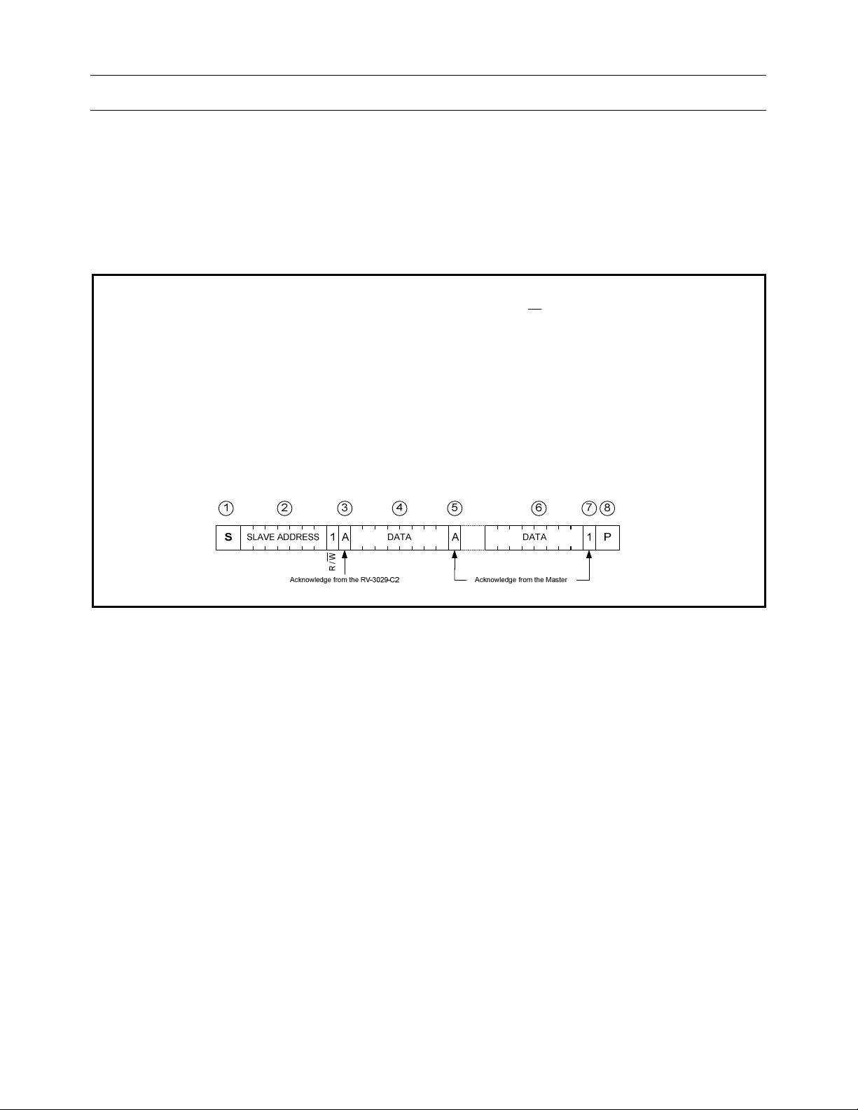
Micro Crystal
DTCXO Temperature Compensated Real Time Clock / Calendar Module RV-3029
6.8.3. READ MODE
• With the first byte, the Master has addressed the RV-3029 in Write Mode
• The Slave becomes the Transmitter and sends out
the
data from the last accessed Page / Word address
incremented by 1
• After reading a byte, within the same Memory-Page the Word-Address is automatically incremented by 1.
If “acknowledge” is not received, no auto increment of the address is executed and a following reading
transmits data of the same address
Example of Reading Data at the last accessed Page & Word address incremented by 1
1)
Master sends out the “Start Condition”
2) Master sends out the “Slave Address”, ADh for the RV-3029; the R/W bit = “1” for read mode
3) Acknowledgement from the RV-3029:
At this point, the Master becomes a Receiver, the Slave becomes the Transmitter
4) The RV-3029 sends out the “Data” from the last accessed Page / Word Address incremented by 1
5) Acknowledgement from the Master
6) Steps 4) and 5) can be repeated if necessary. Within the same Page-Address, the Word-Address will be
incremented by 1 automatically
7) The Master, addressed as Receiver, can stop data transmission by not generating an acknowledge on the
last byte that has been sent from the Slave-Transmitter. In this event, the Slave-Transmitter must leave the
data line HIGH to enable the Master to generate a “Stop condition”
8) Master sends out the “Stop Condition”
53/67

Micro Crystal
DD
DD
DD
ppm
2
2
Start
amb
AMB
DTCXO Temperature Compensated Real Time Clock / Calendar Module RV-3029
7. ELECTRICAL CHRACTERISTICS
7.1. ABSOLUTE MAXIMUM RATINGS
In accordance with the Absolute Maximum Rating System IEC 60134
PARAMETER SYMBOL CONDITIONS MIN. MAX. UNIT
Supply voltage VDD > GND / < VDD GND -0.3 +6.0 V
Supply current I
Input voltage VI Input Pin GND -0.3 V
Output voltage VO
DC Input current II -10 +10 mA
DC Output current IO -10 +10 mA
Total power dissipation P
Operating ambient temperature range T
Storage temperature range T
Electro Static Discharge voltage V
Latch-up current I
1)
HBM: Human Body Model, according to JESD22-A114.
2)
MM: Machine Model, according to JESD22-A115.
3)
Latch-up testing, according to JESD78.
Stresses above these listed maximum ratings may cause permanent damage to the device. Exposure beyond
specified operating conditions may affect device reliability or cause malfunction.
7.2. FREQUENCY AND TIME CHARACTERISTICS
VDD= 3.0 V; VSS= 0 V; T
PARAMETER SYMBOL CONDITIONS TYP. MAX. UNIT
32.768 kHz Oscillator Characteristics
Frequency accuracy
Frequency vs. voltage characteristics
Frequency vs. temperature characteristics
Turnover temperature TO +25 20 - 30 °C
Aging first year max.
Oscillator start-up voltage V
Oscillator start-up time T
Frequency drift vs supply voltage
CLKOUT duty cycle
Time accuracy, DTCXO Digitally Temperature Compensated
Time accuracy Opt: A
Time accuracy Opt: B
= +25°C; f
amb
= 32.768 kHz
OSC
DD ; ISS
V
300 mW
TOT
-40 +125 °C
OPR
Stored as bare product -55 +125 °C
STO
ESD
3)
200 mA
LU
F
∆
f / f
∆
f/(f∆V)
∆
f / T
OPR
∆
f / f T
Start
Start
∆
f/(f∆V)
∆
t / t
∆
t / t
CLKOUT
T
amb
V
T
amb
V
T
OPR
V
amb
T
amb
T
T
amb
T
amb
VDD = 1.4 to 5.5V
T
F
CLKOUT
T
T
amb
T
amb
T
amb
T
amb
T
amb
T
amb
T
amb
T
amb
T
amb
T
amb
Pin -50 +50 mA
DD
+0.3 V
DD
INT / CLKOUT
HBM1)
MM2)
GND -0.5 V
+0.5 V
DD
±2000
±300
= 32.7678 kHz
= +25°C
+/- 10 +/- 20 ppm
= 3.0 V
= +25°C
= 1.4 V to 5.5 V
= -40°C to +125°C
= 3.0 V
+/- 0.5 +/- 1.0 ppm / V
-0.035
/
(T
°C
OPR-T0
(+/-10%)
= +25°C +/- 3 ppm
= +25°C
< 10 s
1.0 V
= -40°C to +85°C 0.5 3
= -40°C to +125°C 1 3
= 25°C
= 32.7678 kHz
= +25°C
0.5 1 ppm
50 40 / 60 %
= +25°C +/-1 +/-3
= 0°C to +50°C +/-2 +/-4
= -10°C to +65°C +/-3 +/-5
= -40°C to +85°C +/-4 +/-6
= -40°C to +125°C +/-5 +/-8
= +25°C +/-1 +/-3
= 0°C to +50°C +/-3 +/-5
= -10°C to +65°C +/-5 +/-10
= -40°C to +85°C +/-10 +/-25
= -40°C to +125°C +/-15 +/-30
V
V
)
ppm
s
ppm
ppm
54/67

Micro Crystal
VDD
=
1.4 V
amb
amb
amb
amb
amb
amb
amb
SCL = 100 kHz
amb
amb
amb
SCL = 400 kHz
amb
amb
amb
amb
DTCXO Temperature Compensated Real Time Clock / Calendar Module RV-3029
7.3. STATIC CHARACTERISTICS
VDD= 1.4 V to 5.5 V; VSS= 0 V; T
PARAMETER SYMBOL CONDITIONS MIN. TYP. MAX. UNIT
Supplies
Supply voltage VDD
Minimum supply voltage detection V
Minimum supply voltage detection V
Main Supply to Backup Supply
Switchover Hysteresis
Supply current
I2C bus inactive
CLKOUT disabled
V
= 0 V
BACK
or
VDD = 0 V
Supply current
I2C bus active
CLKOUT disabled
Current consumption
I2C bus inactive
CLKOUT = 32.768kHz,
C
= 7.5pF
LOAD
Inputs
LOW level input voltage VIL
HIGH level input voltage VIH 80% VDD V
Input leakage current
VSS > VI < VDD
Input capacitance CI 7 pF
Outputs
HIGH level output voltage VOH
LOW level output voltage VOL
HIGH level output current IOH VOH = 4.5 V / V
LOW level output current IOL VOL = 0.8 V / V
Output leakage current ILO
Operating Temperature Range
Operating temperature range T
= -40°C to +125°C; f
amb
Time-keeping mode
I2C bus reduced speed
= 32.768 kHz
OSC
1.4 5.5 V
I2C bus full speed 2.1 5.5 V
T
LOW1
T
LOW2
V
VDD to V
HYST
IDD
(V
= 0 V)
BACK
or
I
BACK
(VDD = 0 V)
IDD
= -40°C to +125°C 1.8 2.1 V
amb
= -40°C to +125°C 1.0 1.4 V
amb
= 3.0 V 20 mV
BACK
T
= -40°C to +85°C
VDD = 1.4 V
T
= -40°C to +125°C
VDD = 3.3 V
T
= -40°C to +85°C
VDD = 3.3 V
T
= -40°C to +125°C
VDD = 5.0 V
T
= -40°C to +85°C
VDD = 5.0 V
T
= -40°C to +125°C
SCL = 100 kHz
VDD = 1.4 V
T
VDD = 1.4 V
T
SCL = 400 kHz
VDD = 3.3 V
T
SCL = 400 kHz
VDD = 3.3 V
T
VDD = 5.0 V
T
SCL = 400 kHz
VDD = 5.0 V
T
= -40°C to +85°C
= -40°C to +125°C
= -40°C to +85°C
= -40°C to +125°C
= -40°C to +85°C
= -40°C to +125°C
0.6 1.5 µA
4.6 µA
0.8 2.0 µA
5.2 µA
0.9 2.2 µA
5.5 µA
12 µA
15 µA
35 µA
40 µA
50 µA
60 µA
VDD = 5.0V 2.5 3.4 µA
I
DD32K
VDD = 3.3V 1.5 2.2 µA
VDD = 1.4V 1.1 1.6 µA
VDD = 1.4 V to 5.0V
Pins: SCL, SDA, CLKOE
T
= -40°C to +85°C
IL
amb
T
= -40°C to +125°C -1.5 +1.5 µA
amb
20% VDD V
-1 +1 µA
VDD = 1.4V; IOH = 0.1mA 1.0
VDD = 5.0V; IOH = 2.0mA 4.5
VDD = 1.4V; IOL = 0.4mA 0.2
VDD = 5.0V; IOL = 5.0mA 0.8
= 5 V 2.0 mA
DD
= 5 V -5.0 mA
VO = V
T
= -40°C to +85°C
VO = V
T
= -40°C to +125°C
-40 +125 °C
OPR
or VSS
DD
or VSS
DD
DD
-1 0 +1
-1.5 0 +1.5
V VDD = 3.3V; IOH = 1.5mA 2.7
V VDD = 3.3V; IOL = 1.5mA 0.25
µA
55/67

Micro Crystal
DTCXO Temperature Compensated Real Time Clock / Calendar Module RV-3029
PARAMETER SYMBOL CONDITIONS MIN. TYP. MAX. UNIT
EEPROM Characteristics
Read voltage V
Programming voltage V
EEPROM Programming Time T
EEPROM Programming Time T
EEPROM Programming Time T
EEPROM write / erase cycles V
T
Read
T
Prog
Prog
Prog
Prog
VDD to V
HYST
= -40°C to +125°C 1.4 V
amb
= -40°C to +125°C 2.2 V
amb
T
= -40°C to +125°C
amb
1 Byte EEPROM User
T
= -40°C to +125°C
amb
1 Byte
EEPROM Control
T
= -40°C to +125°C
amb
2-4 Byte
EEPROM Control
= 3.0 V 5000 Cycles
BACK
35 ms
100 ms
135 ms
Trickle charger
Current limiting resistors
VDD = 5.0V
V
= 3.0V
BACK
R80k T
R20k T
R5k T
R1.5k T
= 25°C 80
amb
= 25°C 20
amb
= 25°C 5
amb
= 25°C 1.5
amb
kΏ
Thermometer
T
= -40°C to +85°C +/-4
Thermometer precision TE
amb
T
= -40°C to +125°C +/-6
amb
°C
7.4. I2C INTERFACE TIMING CHARACTERISTICS
56/67

Micro Crystal
DTCXO Temperature Compensated Real Time Clock / Calendar Module RV-3029
VSS= 0 V; T
= -40°C to +125°C. All timing values are valid within the operating supply voltage range and
amb
references to VIL and VIH with an input voltage swing from VSS to VDD.
PARAMETER SYMBOL CONDITIONS MIN MAX UNIT
VDD ≥ 1.4V 100
SCL Clock Frequency f
Start Condition Set-up Time t
Start Condition Hold Time t
Data Set-up Time t
Data Hold Time t
Data Valid Time t
Data Valid Acknowledge Time t
Stop Condition Set-up Time t
Bus Free Time between STOP and START condition t
SCL “LOW time” t
SCL “HIGH time” t
SCL and SDA Rise Time tr
SCL and SDA Fall Time tf
Tolerance Spike Time on Bus tSP 50 ns
SCL and SDA I/O Capacitance C
Capacitive Load Bus Lines CB 200 pF
SCL
VDD ≥ 3.0V 400
VDD ≥ 1.4V 50
SU ; STA
VDD ≥ 3.0V 20
VDD ≥ 1.4V
HD ; STA
0.2 µs VDD ≥ 1.8V
VDD ≥ 3.0V
VDD ≥ 1.4V 100
SU ; DAT
VDD ≥ 3.0V 50
VDD ≥ 1.4V 50
HD ; DAT
VDD ≥ 3.0V 20
VDD ≥ 1.4V 4.0
VD ; DAT
VDD ≥ 3.0V 1.2
VDD ≥ 1.4V 3.5
VD ; ACK
VDD ≥ 3.0V 0.9
VDD ≥ 1.4V 50
SU ; STO
VDD ≥ 3.0V 20
VDD ≥ 1.4V 1.0
BUF
VDD ≥ 3.0V 0.4
VDD ≥ 1.4V 4.5
LOW
VDD ≥ 3.0V 1.3
VDD ≥ 1.4V 0.6
HIGH
VDD ≥ 3.0V 0.4
VDD ≥ 1.4V 1.0
VDD ≥ 3.0V 0.2
VDD ≥ 1.4V 0.4
VDD ≥ 3.0V 0.2
I/O
10 pF
kHz VDD ≥ 1.8V 300
µs VDD ≥ 1.8V 30
ns VDD ≥ 1.8V 80
ns VDD ≥ 1.8V 30
µs VDD ≥ 1.8V 1.5
µs VDD ≥ 1.8V 1.1
ns VDD ≥ 1.8V 30
µs VDD ≥ 1.8V 0.5
µs VDD ≥ 1.8V 1.7
µs VDD ≥ 1.8V 0.5
µs VDD ≥ 1.8V 0.3
µs VDD ≥ 1.8V 0.3
57/67
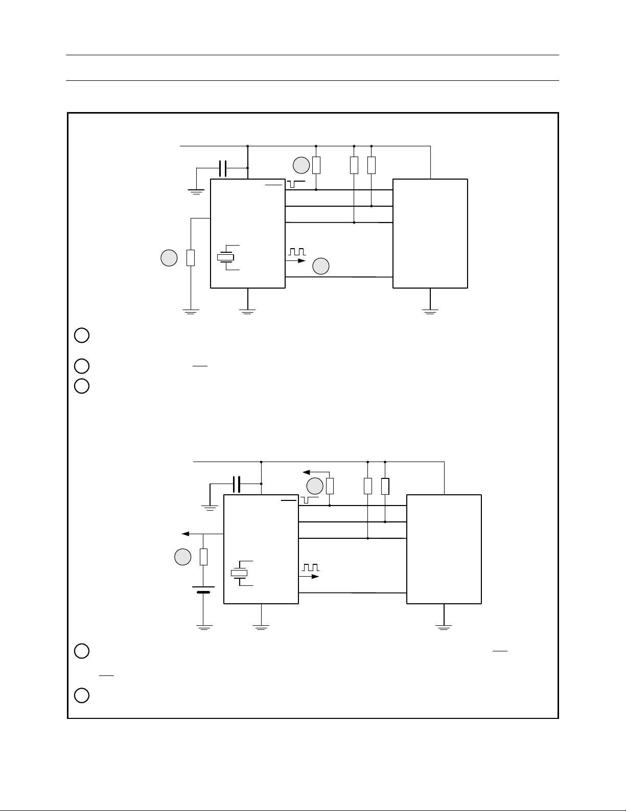
Micro Crystal
INT
INT
INT
DTCXO Temperature Compensated Real Time Clock / Calendar Module RV-3029
8. APPLICATION INFORMATION
Operating RV-3029 without V
V
DD
10 nF
BACKUP
V
BACKUP
Supply:
V
DD
RV-3029
INT
SDA
SCL
2
INT
SDA
SCL
µ Controller
1
CLKOUT
CLKOE
V
SS
3
GPIO
V
SS
1
When operating the RV-3029 without Backup Supply Voltage, it is recommended to tie V
10 kOhm resistor is recommended.
2
Pull-up resistor of the
3
CLKOUT is enabled when CLKOE input is high. It either can be permanently enabled with a pull-up resistor
signal can be tied directly to supply voltage V
DD.
BACKUP
pin to GND,
to supply voltage VDD or actively controlled by the µController.
If no clock function is needed, it is recommended to disable CLKOUT by permanently tie CLKOE pin with a
pull-down resistor to GND.
Operating RV-3029 with Backup Supply Voltage V
V
DD
10 nF
V
BACKUP
BACKUP
:
4
V
V
BACKUP
DD
INT
SDA
V
BACKUP
5
RV-3029
SCL
INT
SDA
SCL
µ Controller
CLKOUT
CLKOE
V
SS
GPIO
V
SS
4
When operating the RV-3029 with either Supercap or Lithium Battery as Backup Supply, the
also works when the device operates on V
5
pull-up resistor to V
BACKUP.
When a Lithium Battery is used, it is recommended to insert a protection resistor of 100 - 1’000 Ohm to
supply voltage. Therefore it is recommended to tie the
BACKUP
signal
limit battery current and to prevent damage in case of soldering issues causing short between supply pins.
58/67

Micro Crystal
Temperature Profile
Symbol
Condition
Unit
max
cool
to-peak
Preheat
min
max
min
max
Soldering above liquidus
Peak temperature
DTCXO Temperature Compensated Real Time Clock / Calendar Module RV-3029
8.1. RECOMMENDED REFLOW TEMPERATURE (LEADFREE SOLDERING)
Maximum Reflow Conditions in accordance with IPC/JEDEC J-STD-020C “Pb-free”
Average ramp-up rate (Ts
Ramp down Rate T
Time 25°C to Peak Temperature T
to Tp) 3°C / second max °C / s
6°C / second max °C / s
8 minutes max m
Temperature min Ts
Temperature max Ts
Time Ts
to Ts
ts 60 - 180 Sec
150 °C
200 °C
Temperature liquidus TL 217 °C
Time above liquidus tL 60 – 150 sec
Peak Temperature Tp 260 °C
Time within 5°C of peak temperature tp 20 - 40 sec
59/67

Micro Crystal
DTCXO Temperature Compensated Real Time Clock / Calendar Module RV-3029
9. PACKAGES
9.1. DIMENSIONS AND SOLDERPADS LAYOUT
C2 Package:
Package dimensions (bottom view): Recommended solderpad layout:
C3 Package:
Package dimensions (bottom view): Recommended solderpad layout:
All dimensions in mm typical.
60/67

Micro Crystal
DTCXO Temperature Compensated Real Time Clock / Calendar Module RV-3029
9.2. MARKING AND PIN #1 INDEX
C2 Package:
C3 Package:
61/67
Micro Crystal
DTCXO Temperature Compensated Real Time Clock / Calendar Module RV-3029
10. PACKING INFORAMTION
10.1. CARRIER TAPE
12 mm Carrier-Tape: Material: Polystyrene / Butadine or Polystyrol black, conductive
Cover Tape: Base Material: Polyester, conductive 0.061 mm
Adhesive Material: Pressure-sensitive Synthetic Polymer
C2 Package:
C3 Package:
Tape Leader and Trailer: 300 mm minimum.
All dimensions in mm.
User Direction of Feed
62/67

Micro Crystal
Reels
: Diameter
Material
RTC’s per reel
Reels:
Diameter
Material
RTC’s per reel
DTCXO Temperature Compensated Real Time Clock / Calendar Module RV-3029
10.2. PARTS PER REEL
C2 Package:
7” Plastic, Polystyrol 1’000
13” Plastic, Polystyrol 5’000
C3 Package:
7” Plastic, Polystyrol 1’000
7” Plastic, Polystyrol 3’000
63/67

Micro Crystal
Reel:
DTCXO Temperature Compensated Real Time Clock / Calendar Module RV-3029
10.3. REEL 13 INCH FOR 12 mm TAPE
Diameter Material
13” Plastic, Polystyrol
64/67

Micro Crystal
Reel:
DTCXO Temperature Compensated Real Time Clock / Calendar Module RV-3029
10.4. REEL 7 INCH FOR 12 mm TAPE
Diameter Material
7” Plastic, Polystyrol
65/67

Micro Crystal
DTCXO Temperature Compensated Real Time Clock / Calendar Module RV-3029
11. HANDLING PRECAUTIONS FOR CRYSTALS OR MODULES WITH EMBEDDED
CRYSTALS
The built-in tuning-fork crystal consists of pure Silicon Dioxide in crystalline form. The cavity inside the package is
evacuated and hermetically sealed in order for the crystal blank to function undisturbed from air molecules,
humidity and other influences.
Shock and vibration:
Keep the crystal / module from being exposed to excessive mechanical shock and vibration. Micro Crystal
guarantees that the crystal / module will bear a mechanical shock of 5000g / 0.3 ms.
The following special situations may generate either shock or vibration:
Multiple PCB panels - Usually at the end of the pick & place process the single PCBs are cut out with a router.
These machines sometimes generate vibrations on the PCB that have a fundamental or harmonic frequency
close to 32.768 kHz. This might cause breakage of crystal blanks due to resonance. Router speed should be
adjusted to avoid resonant vibration.
Ultrasonic cleaning - Avoid cleaning processes using ultrasonic energy. These processes can damages
crystals due to mechanical resonance of the crystal blank.
Overheating, rework high temperature exposure:
Avoid overheating the package. The package is sealed with a seal ring consisting of 80% Gold and 20% Tin. The
eutectic melting temperature of this alloy is at 280°C. Heating the seal ring up to >280°C will cause melting of the
metal seal which then, due to the vacuum, is sucked into the cavity forming an air duct. This happens when using
hot-air-gun set at temperatures >300°C.
Use the following methods for rework:
• Use a hot-air- gun set at 270°C.
• Use 2 temperature controlled soldering irons, set at 270°C, with special-tips to contact all solder-joints from
both sides of the package at the same time, remove part with tweezers when pad solder is liquid.
66/67

Micro Crystal
DTCXO Temperature Compensated Real Time Clock / Calendar Module RV-3029
12. DOCUMENT REVISION HISTORY
Date Revision # Revision Details
April 2010 1.2 First release
July 2010 1.3 Modified EEPROM Programming Time
June 2011 1.4 Modified EEPROM Memory Access
March 2012 2.0 Add C3 package version
Information furnished is believed to be accurate and reliable. However, Micro Crystal assumes no
responsibility for the consequences of use of such information nor for any infringement of patents or other
rights of third parties which may result from its use. In accordance with our policy of continuous
development and improvement, Micro Crystal reserves the right to modify specifications mentioned in this
publication without prior notice. This product is not authorized for use as critical component in life support
devices or systems.
67/67
 Loading...