

Page 1
1997 Microchip Technology Inc.
Preliminary
DS40150B-page 1
M
SCS152
FEATURES
• ISO 7816-3:1989 “Answer to Reset” compatible
for synchronous cards
• Industry standard 4406 command set compatible
• Extended commands:
- Combined WRITE and
ERASE-WITH-CARRY function
- Cryptographic signature of the EEPROM
contents and challenge
• 40-bit user programmable area with lock bit
• 64-bit cryptographic key
• 64-bit transport code
• 33352 token units (78888
8
)
• Internal protection against token counter value
corruption (anti-tearing)
DESCRIPTION
The SCS152 is a third generation token card integrated
circuit intended for prepaid applications. Typical applications of the SCS152 include disposable telephone
cards, vending machine cards, low value debit cards,
access control, and authentication.
The SCS152 incorporates several security features,
including an internal signature function and a long
transport code. The SCS152 has two modes – issuer
mode and user mode. During wafer testing, it is placed
in issuer mode for card manufacturing and transportation to the issuer. In issuer mode, the transport code is
needed to program the device and, thus, is protected
from unauthorized use before personalization by the
issuer.
During personalization, a cryptographic key, unique to
the card, is programmed into EEPROM. This key can
not be read. The system using the card must be able to
determine what key was programmed from examining
the memory map (i.e., not the token counter) containing
the issuer and serial number information.
The signature function computes an 8-bit value based
on a system supplied value (challenge) and the visible
memory map. Because of the nature of the signature
function and the fact that the key is not known outside
the system, it is practically impossible to predict the
value which the signature will compute.
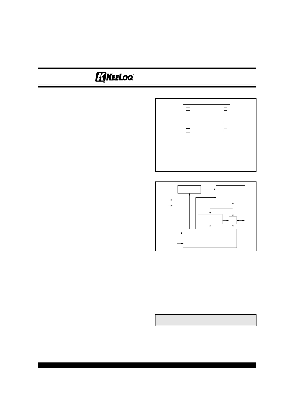
DIE LAYOUT
BLOCK DIAGRAM
A correct signature indicates that the memory contents
have not been altered. It can theref ore be used to check
the serial number, or that changes to the token counter
have actually occurred.
Programming the token counter uses a special circuit to
ensure that the programming will either be complete or
will not happen at all, if the external supply is suddenly
removed.* This is called Fail Safe Programming™ ,
and, when used in conjunction with the extended write
and erase command, removes the need for special
‘tear-out’ protection to be performed by the reader.
Note: The fail safe f eature only works in the token
counter area.
GND
SDIO
VDD
SCI
SCK
I/O
SCI
SCK
SDIO
VDD
GND
ADDRESS
GENERATION
EEPROM
SIGNATURE
CALCULATOR
CONTROLLER
Token Card Chip
K
EE
L
OQ
is a registered trademark of Microchip Technology Inc.
*Patents applied for.
Page 2
SCS152
DS40150B-page 2
Preliminary
1997 Microchip Technology Inc.
1.0 PIN DEFINITIONS
2.0 DEVICE OPERATION
During the life of the SCS152, it goes through the following stages:
• Manufacture and wafer probing
• Waffle pack and transportation
• Personalization and final application.
Various fields in the memory map must be initialized.
These include the first 24 bits in the memory map, the
transport code, and the mode bits. The first 24 bits in
the memory map typically identifies the device in its
final application. The device has two principle modes:
issuer mode and user mode. In issuer mode , all access
to the device (except one field) is b locked before a correct transport code has been presented to the device.
Thus, the transport code protects the device against
theft, before it is personalized.
During personalization, all fields, except (Chip
Identification Data (CID), are initialized for the intended
application: the device serial number is programmed,
the token counter is set to its proper value, the user
data field is initialized, and the transport code is erased
and replaced with a cryptographic key.
After power has been applied to the device, the I/O pin
is driven low . Once the reset period (T
POR
) has expired,
the SCS152 is ready to accept commands. These commands typically read the memory content serially. The
first bit at address 0 is initially driven on the I/O line.
Each read clock pulse increments the internal address
counter and reads the resulting bit from EEPROM. This
serial data stream is composed of various fields presented in Table 2-1.
2.1 C
ID Field
The device CID field contains a device identification
code, which is programmed during wafer probe and
cannot be changed later. These bits typically identify
the type of the device to the system in the application.
2.2 SER Field
The SER field contains the device serial number which
identifies the individual device. It is programmed while
the device is in issuer mode during the personalization
stage.
2.3 ISS Field
The ISS field indicates whether the device is in issuer
mode as determined by the CFG field. This is purely an
external view of the CFG field and exists as such for
compatibility reasons.
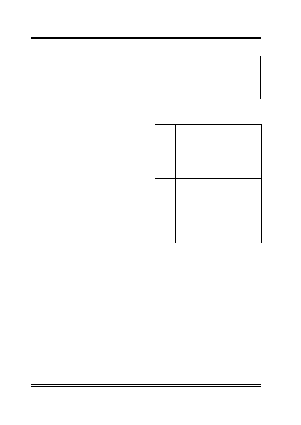
ISO Pin Name I/O Type Description
C1 V
DD
Power Power connection
C2 SCI INPUT Command input to the device controller
C3 SCK INPUT Command execution clock input
C5 GND Power Power connection
C7 SDIO Bidir (O.D.) Open drain serial data I/O line
TABLE 2-1: EXTERNAL
REPRESENTATION OF THE
INTERNAL MEMORY MAP
Field
Name
Address Size Description
CID 0…23 24 Chip identification
data
SER 24…63 40 Serial number
ISS 64 1 Issuer mode status
D4 65…71 7 Digit 4
D3 72…79 8 Digit 3
D2 80…87 8 Digit 2
D1 88…95 8 Digit 1
D0 96…103 8 Digit 0
CFG 104…107 4 Configuration data
USER0 108…147 40 User area
UKEY0 148…211 64 Key area 0 which
also acts as the
transport code in
issuer mode
212…275 64 Undefined
Page 3
SCS152
1997 Microchip Technology Inc.
Preliminary
DS40150B-page 3
2.4 Digit Fields
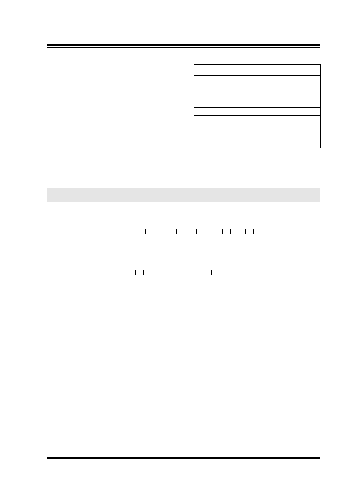
2.4.1 DIGIT FIELD VALUE
Each digit field, D4 to D0, represents a number equal to
the number of ‘1’ bits in the field. Table 2-2 shows the
value of the digit field for each legal digit value.
TABLE 2-2: DIGIT FIELD VALUES
2.4.2 TOKEN COUNTER VALUE
The following formula shows how the digit fields combine to form the token counter value:
This is, in fact, an octal representation of a value and can be written as:
Suppose the 5-digit field contain the values: (D4=3), (D3=0), (D2=7), (D1=1), (D0=3). The token counter value is then
30713
8
in octal or in decimal:
A digit needs to be set to eight to handle the borrow from the next higher stage. This also implies that each counter v alue
does not have a unique representation. For example, 00500
8
= 5 x 64 = 320
10
or 00480
8
or 00478
8
.
Digit Value Field Value
0 0000 0000
1 1000 0000
2 1100 0000
3 1110 0000
4 1111 0000
5 1111 1000
6 1111 1100
7 1111 1110
8 1111 1111
Note: The bits are shown, right to left, in the order
in which they are read out.
Note: The value digit D4 is shown in the formulas as |D4| indicating the number of 1 bits in the digit D4 field.
Similarly |D3| indicates the number of 1 bits in the digit D3 field, and so on.
Tokens D4 4096 D3 512 D2 64 D1 8 D0+×+×+×+×=
Tokens D4 84D3 83D2 82D1 81D0 80×+×+×+×+×=
Tokens 3 4096 0 512 7 64 1 8 3+×+×+×+× 12747
10
= =
Page 4

SCS152
DS40150B-page 4
Preliminary
1997 Microchip Technology Inc.
2.5 CFG Field
The CFG field is further divided into four subfields:
With ‘PC0 = 0’ and ‘PC1 = 1’, the device is in issuer
mode; with ‘PC0 = 1’ and ‘PC1 = 0’, the de vice is in user
mode. Some commands can only be used in issuer
mode.
2.6 USER0 Field
The user area can be reprogrammed to any state by the
user in user mode. It also can be locked using the
LOCK0 bit. In issuer mode, this field typically contains
the packaging status of the device. In user mode, this
field can be used for application dependent data.
2.7 UKEY0 Field
In issuer mode, this field contains the transport code; in
user mode, the UKEY0 field contains the key used in
the signature function. The transport code is
programmed during wafer probe and is completely
reprogrammed during personalization to the value of
the key.
3.0 COMMAND INTERFACE
The SCS152 accepts the following basic commands:
RESET, RDBIT/PUTBIT, BITPROG and ERASE. The
extended commands are DECR-ERASE and initiate
signature function.
The device interprets five different SCI/SCK sequences
for all its commands:
a) An overlap of SCI and SCK for RESET
b) A single pulse on SCK for RDBIT or PUTBIT
c) A single pulse on SCI followed by a pulse on
SCK for BITPROG
d) A repeat of c) for ERASE
e) A double pulse on SCI followed by a pulse on
SCK for extended commands
Normally, any one of these sequences can be followed
by another; however, once the signature function has
been started, a fixed sequence of commands must follow.
The extended functions are accessed by double pulse
on SCI in the correct address range. Depending on the
current address, the same sequence of events on SCI
and SCK will perform different functions.
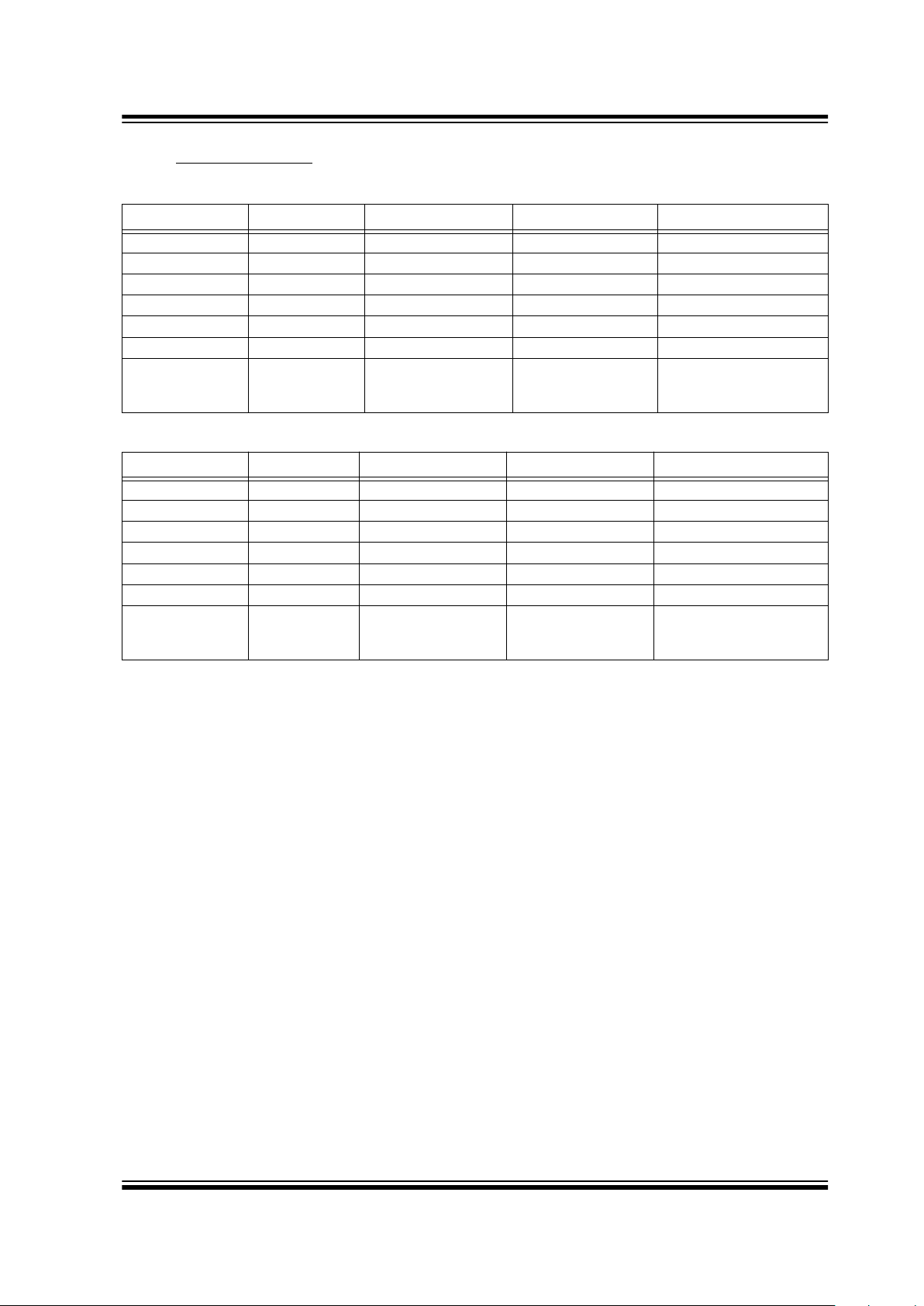
Name Address Description
PC0 104 First bit of the issuer mode/user
mode indicator
PC1 105 Second bit of the issuer mode/
user mode indicator
N.U. 106 Unused
LOCK0 107 Unlocked status of USER0 area
in user mode: ‘0’ means locked
TABLE 3-1: EXTENDED FUNCTIONS
Field
Extended Function Accessed by
Double SCI Pulse
CID Test modes
SER BITPROG
D4…D0 DECR-ERASE
CFG Test modes
USER0 BITPROG
UKEY0 Address 163: test mode
Address 259: Initiate signature operation
Other addresses perform BITPROG
Page 5
SCS152
1997 Microchip Technology Inc.
Preliminary
DS40150B-page 5
3.1 Access Condition
s
The condition codes are:
Note 1: If the access condition does not allow a command that modifies the EEPROM (i.e., BITPROG, ERASE or
DECR-ERASE), it will be converted into a RDBIT command.
2:
The commands that can potentially change the EEPROM (ev en if it is conv erted into a RDBIT command) do
not increment the I/O address counter.
3:
Any command that modifies the EEPROM checks the internal high voltage sensor during the programming
and goes into the standby state if the sensor indicates the internal high voltage was not high enough. Power
must be removed to clear this condition.
4:
If the device is not in issuer mode and not in user mode, only BITPROG access is allowed to the CFG field.
TABLE 3-2: ACCESS CONDITIONS IN ISSUER MODE
Field RDBIT BITPROG ERASE Extended Commands
CID Y F and TC N test modes
SER Y TC N BITPROG
O4…O1 Y TC and Z TC and B DECR-ERASE: TC and Z
O0 Y TC and Z N N
CFG Y TC N test modes
USER0 Y Y Y BITPROG
UKEY0 ‘1’ TC TC
BITPROG
test modes
SIGN: Y
TABLE 3-3: ACCESS CONDITIONS IN USER MODE
Field RDBIT BITPROG ERASE Extended Commands
CID Y N N test modes
SER Y N N BITPROG
O4…O1 Y Z B DECR-ERASE: Z
O0 Y Z N N
CFG Y Y N test modes
USER0 Y L L BITPROG
UKEY0 ‘1’ N N
BITPROG
test modes
SIGN: Y
• Y Command always allowed
• N No access allowed and it is converted into a RDBIT command
• TC Transport code must be submitted before the operation is allowed
• ‘1’ Output always logic high in this field
• F Command allowed if the fuse is not blown
• Z The digit code is nonzero
• B Command allowed if previous operation was BITPROG and was successfully
• L Command allowed if LOCK0 bit in the CFG field is ‘1’
• BITPROG The BITPROG condition is checked and executed
Page 6

SCS152
DS40150B-page 6
Preliminary
1997 Microchip Technology Inc.
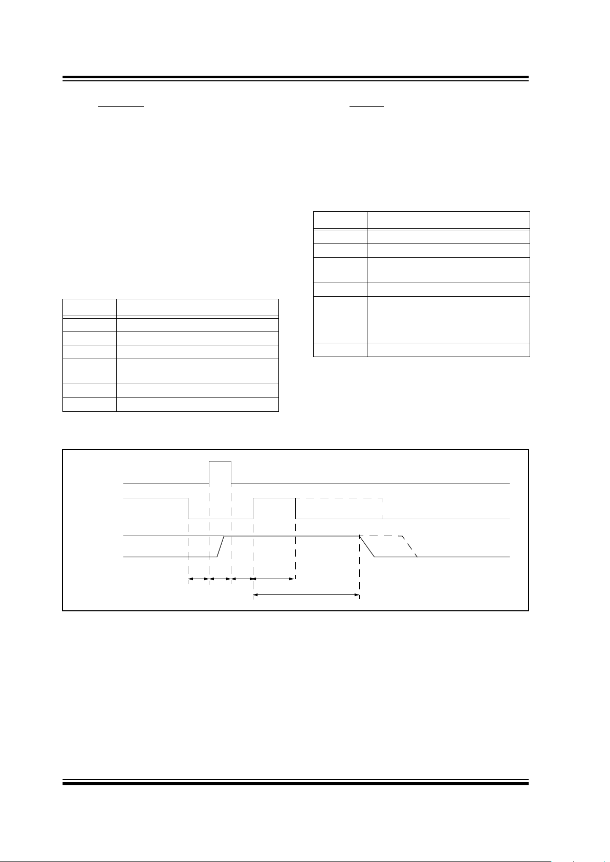
3.2 RESET
The RESET command sets the internal state of the
device as follows:
1. The internal address counter is set to ‘0’.
2. The internal test modes are cleared.
3. The result of the last compared transport code is
cleared.
Figure 3-1 shows the RESET command following the
application of power.
FIGURE 3-1: POWER ON AND RESET
VDD
SCI
SCK
SDIO
IOMAP(0)
TPOR TR TOXTOX TD1
Page 7

SCS152
1997 Microchip Technology Inc.
Preliminary
DS40150B-page 7
3.3 RDBIT/PUTBIT
The RDBIT command increments the internal address
counter on the leading edge of the SCK pulse and
reads the resulting bit in EEPROM. This SDIO line is
updated on the falling edge of the SCK pulse. If the ne w
address is in the UKEY0 area, the SDIO line will be
tri-stated immediately in preparation of transport code
entry, even if the device is in user mode. Figure 3-2
shows two consecutive RDBIT commands.
The PUTBIT command mirrors a RDBIT command, but
data is transmitted to the chip instead of transmitting
data from the chip. It also increments the internal
address counter. PUTBIT is used to enter the transport
code in issuer mode and the challenge bits, during
signature computation. Figure 3-3 shows data entry,
typically during transport code entry.
FIGURE 3-2: RDBIT
FIGURE 3-3: DATA ENTRY (TRANSPORT CODE DETAIL)
SCI
SCK
SDIO
THTL
IOMAP(n)IOMAP(n-1)
TD2
TH
SCI
SCK
SDIO
TH Tl
IOMAP(147)
TD3 TC
TC(0) TC(1)
TH
Page 8
SCS152
DS40150B-page 8
Preliminary
1997 Microchip Technology Inc.
3.4 BITPR
OG
The BITPROG command modifies one bit in the
EEPROM. In the digit area, this command decrements
the current digit or in the CFG field it programs the bits
to AD(0) xor FUSE-BLOWN state: PC0 is erased to a
‘1’; PC1 is written to a ‘0’; LOCK0 is written to a ‘0’,
when the fuse is in blown state. Everywhere else in the
memory map, the current bit is written to a ‘0’.
Figure 3-4 diagrams the BITPROG command.
This command is signaled by pulsing SCI high. If the
operation is allowed, the SDIO line goes high. The
actual EEPROM modification is initiated by pulsing
SCK high. When the programming operation has been
completed, and SCK is low, the output goes low, indicating that the command has completed.
3.5 ERASE
The wavef orms for ERASE are the same as BITPR OG;
the command is implicitly coded by the repetition of the
sequence of events.
The ERASE command executes different functions,
depending on the current address as shown in
Table 3-5:
FIGURE 3-4: BITPROG
TABLE 3-4: BITPROG FUNCTIONS
Field Description
CID Writes current bit to ‘0’
SER Writes current bit to ‘0’
D4…D0 Decrements the current digit
CFG
Program the current bit to the value of
(AD(0) xor FUSE-BLOWN)
USER0 Writes current bit to ‘0’
UKEY0 Writes current bit to ‘0’
TABLE 3-5: ERASE FUNCTIONS
Field Description
CID —
SER —
O4…O1 Sets the next digit to the maximum digit
value
CFG —
USER0
0x6C…0x73: Erases current nibble to
all ‘1’ state
0x74…0x93: Erases the current b yte to
all ‘1’ state
UKEY0 Erases the current byte to all ‘1’ state
SCI
SCK
SDIO
T
HTS TCTC
TPROG
Page 9

SCS152
1997 Microchip Technology Inc. Preliminary DS40150B-page 9
3.6 DECR-ERASE
The DECR-ERASE command combines BITPROG
and ERASE in the digit area into one operation. It is
only allowed if both of these operations are allowed at
the current address. Figure 3-5 shows the typical
waveforms for the DECR-ERASE command.
FIGURE 3-5: EXTENDED FUNCTIONS MODIFYING EEPROM
SCI
SCK
SDIO
T
HTS TCTCTSTC
TPROG
Page 10

SCS152
DS40150B-page 10 Preliminary 1997 Microchip Technology Inc.
4.0 SIGNATURE FUNCTION
The signature function combines a system-supplied
value with the contents of the memory map to form an
8-bit value. Because UKEY0 is not known and the way
in which these values are combined, it is very difficult to
duplicate.
The signature function can, therefore, be used for a
variety of security related functions, including user/card
authentication and protecting against communication
tampering.
4.1 Signature Procedure
The following procedure controls the device to compute
a signature of the EEPROM contents:
1. Issue a RESET command.
2. Issue 259 RDBIT commands.
3. Pulse SCI high twice.
4. Issue 16 PUTBIT commands to enter the first 16
bits of the challenge.
5. Issue 128 RDBIT commands.
Note: The bits read are the first 128 bits in the
EEPROM without any output mapping;
these bits must be used in checking the
result of the signature function.
6. Issue 16 PUTBIT commands to enter the second 16 bits of the challenge.
7. Wait for the signature computation to complete.
8. Issue 8 RDBIT command to read the result of
the signature computation.
9. Updating the token counter.
4.2 Subtraction Procedure
The following procedure can be used to subtract a
number of tokens:
1. Read the token counter value.
2. Convert the token counter value into an octal format.
3. Con vert the number of tokens to subtract into an
octal format.
4. Do the subtraction using ‘long subtraction’ making note of the borrows.
Note: If the subtraction generated a borrow from
digit 4, the token counter is smaller than the
number subtracted.
5. To update each digit in the order they are read
out (i.e., D4, then D3, then D2, etc.):
a) Calculate by how much this digit must be
decremented. If, during subtraction, a
borrow was generated from this digit to the
next higher digit, the decrement amount is
eight minus this digit’s final value, else it is
its initial value minus its final value.
b) Read to the first ‘1’ bit in the field.
c) If the following digit generated a borrow from
this digit, issue a BITPROG command, fol-
lowed by an ERASE command. (See
Section 5.1 on fail safe counter updating.)
d) Decrement this digit as many times as cal-
culated in Step 5a, taking into account that
Step 5c may already have decremented this
digit. Each decrement is done by reading
the next bit in the field and issuing
a BITPROG command.
EXAMPLE 4-1: SUBTRACT EXAMPLE
Suppose the token counter contains 307138, and 20
10
(248) tokens must be deducted from the counter . Using
‘long subtraction’ to do the calculation the result is
30677
8
.
Note the borrows from digits D2 and D1.
Digits 4 and 3 do not change. The sequence of com-
mands to update digit 2 is: read the second bit in the
field to field D2, BITPROG, and ERASE. The ERASE
command is required because of the borrow.
Updating digit ‘1’ requires the following sequence of
commands: read the first bit to field D1, BITPROG,
ERASE, RDBIT, and BITPROG. Once again, the
ERASE command is required because of the borrow.
Updating digit ‘0’ requires the sequence of commands:
read the first bit to field D0 and BITPROG.
EXAMPLE 4-2: DECREMENTING 320:
Updating this token counter goes through the following
values: 00400
8
, after the first BITPROG; 004808, after
the ERASE; 00470
8
,after BITPROG; 004788,after the
ERASE; 00477
8
, after the final BITPROG.
Note: The final BITPROG actually decrements
the value.
30713
8
00024
8
30667
8
-----------------
00500
8
00001
8
00477
8
-----------------
Page 11

SCS152
1997 Microchip Technology Inc. Preliminary DS40150B-page 11
5.0 COMPATIBILITY WITH
INDUSTRY STANDARD
DEVICES
The RESET and RDBIT commands meets the requirements of ISO 7816-3 for the ‘Answer-to-Reset’
sequence for synchronous chip cards.
The basic counter modification commands BITPROG
and ERASE correspond with the WRITE and
ERASE-WITH-CARRY commands of industry standard
devices. However, industry standard devices use eight
bits to represent each digit, and a WRITE command will
program the current bit to ‘0’.
The application can, therefore, decrement a digit by
programming any of the eight bits to ‘0’, whereas with
the SCS152, any BITPROG command will always
decrement the current digit value. If the application
decrements each digit as described above, the WRITE
command will appear to program the current bit to ‘0’.
Thus, while the SCS152 will accept and interpret the
commands correctly, the changes to the memory map
will only correspond to that of the other cards, if the first
‘1’ in a digit field is always programmed ‘0’ with a
WRITE command.
For example, if digit fi eld D3 contains the value ‘6’, it will
be read out as 00111111. If a BITPROG command is
issued anywhere in D3, its value will be decremented to
‘5’, and it will always read out as 00011111, regardless
of which address in the digit the BITPROG command
was issued.
The ISS is only an external view of the CFG field and
cannot be changed. A BITPROG command at this
address will actually decrement digit D4. It should also
be noted that the address counter appears to wrap from
275 back to 0, which differs from other similar devices.
5.1 Fail Safe Counter Update
The carry is performed by a BITPROG, followed by an
ERASE. This process first deducts a number of tokens
(the BITPROG command) and then adds some again
(with the ERASE command), but never more than previously deducted with the BITPROG command. If the
device is pulled from the reader between the BITPROG
and ERASE commands, the user may lose many
tokens.
This situation can be avoided by substituting the
DECR-ERASE command whenever a sequence of
BITPROG and ERASE commands are needed to
update the token counter (Step 5c in Section 4.2). This
will modify the contents of the EEPROM in one indivisible operation that will either complete or not modify the
EEPROM in any wa y , if e xternal power is remov ed early
on during the EEPROM programming.
Page 12

SCS152
DS40150B-page 12 Preliminary 1997 Microchip Technology Inc.
6.0 PERSONALIZATION
During the typical life of the device, it must be personalized. The following procedure personalizes the
device:
1. Issue a RESET command.
2. Issue 147 RDBIT commands.
3. Issue 64 PUTBIT commands to present the
transport code.
4. Issue 88 RDBIT commands.
5. Program the SER field by issuing BITPROG
commands at the appropriate addresses.
6. Decrement each digit in the token counter to the
proper value by issuing BITPROG and RDBIT
commands as needed.
7. Program the USER area.
8. Program the UKEY0 area by clocking to the first
bit of each byte (i.e., addresses 148, 156,
164, …) issuing BITPROG and ERASE commands, and then programming the byte with
BITPROG commands.
9. Check the contents via the signature function.
10. Set the device to user mode by issuing
a BITPROG commands at addresses 104 and
105.
7.0 MEMORY CONTENTS
7.1 Shipped Devices
7.2 After Personalization
Note: The internal transport code OK status bit is
reset by the RESET command or when the
device is no longer in issuer mode (which
happens when PC0 and PC1 are programmed).
Field Name Contents
CID Chip identification data
SER all 1
ISS 1
D4 all 1
D3 all 1
D2 all 1
D1 all 1
D0 all 1
CFG PC0 = 0, PC1 = 1, LOCK0 = 1
USER0 All 1
UKEY0 Transport code
Field Name Contents
CID Chip identification data
SER Device serial number
ISS 0
D4 Digit 4 of counter
D3 Digit 3 of counter
D2 Digit 2 of counter
D1 Digit 1 of counter
D0 Digit 0 of counter
CFG PC0 = 1, PC1 = 0,
LOCK0 = 1/0 depending on application
USER0 All 1
UKEY0 Transport code
Page 13
SCS152
1997 Microchip Technology Inc. Preliminary DS40150B-page 13
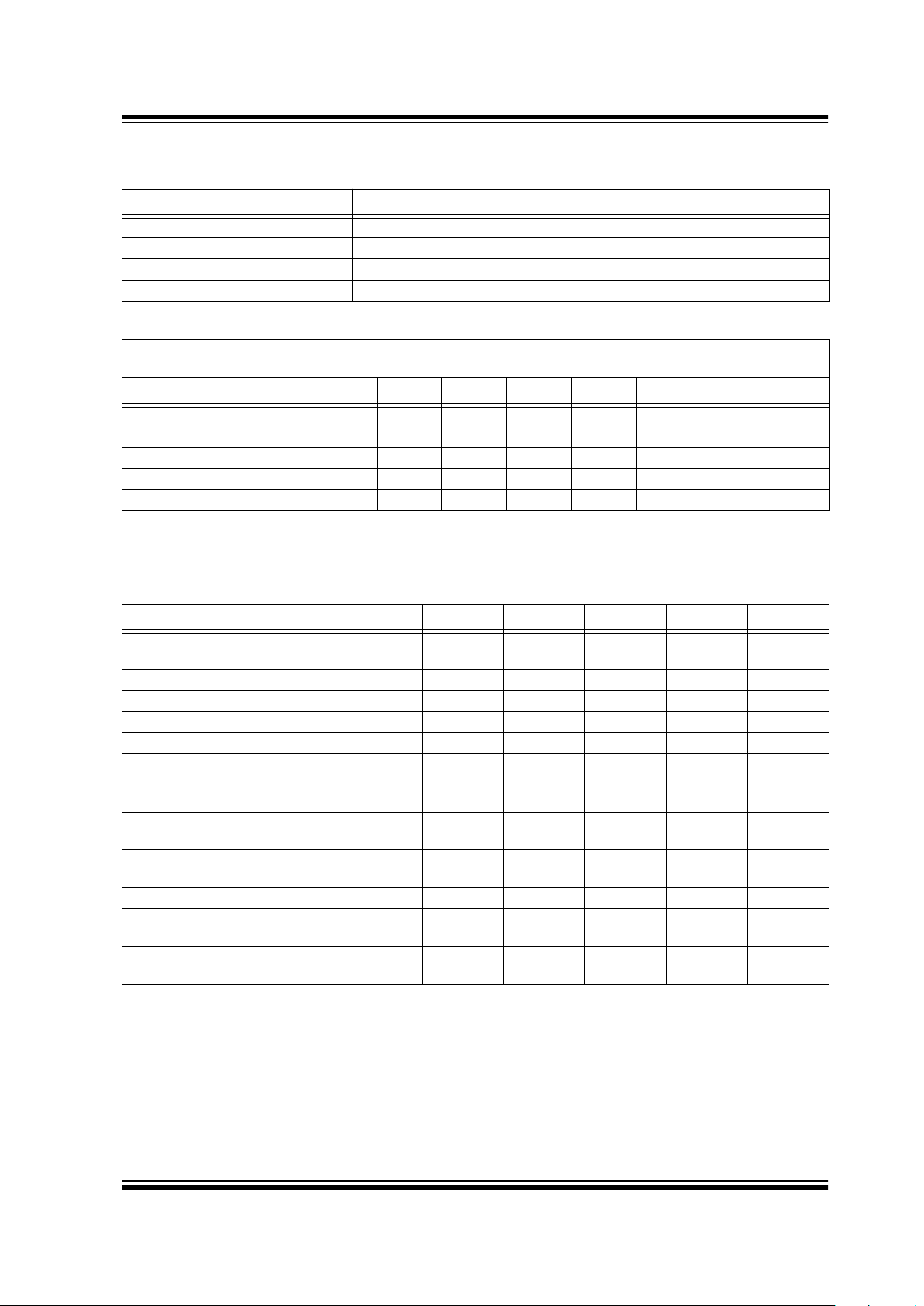
8.0 DEVICE CHARACTERISTICS
TABLE 8-1: ABSOLUTE MAXIMUM RATINGS
Description Symbol Min. Max. Units
Supply voltage, with respect to GND V
DD -0.3 6.0 V
Input voltage, with respect to GND V
I -0.3 6.0 V
Storage temperature T
S -55 +85 °C
ESD protection on all pins (HBM) V
ESD — 4000 V
TABLE 8-2: DC CHARACTERISTICS
VDD: 5.0 V ± 10%
T
A: -40°C to +85°C
Description Symbol Min. Typ. Max. Units Condition
Current when reading I
DDR — 300 600 µA SDIO = VDD
Current when programming IDDP — 1.2 1.6 mA SDIO = VDD
Input low voltage VIL — — 0.8 V
Input high voltage V
IH 3.0 — — V
Output low voltage V
OL — — 0.4 V Sinking current, Io = 1 mA
TABLE 8-3: AC CHARACTERISTICS
VDD: 5 V ± 10%
T
A: -40°C to +85°C
R
PU = 10K
Description Symbol Min. Typ. Max. Units
Time from V
DD high until device accepts com-
mands
T
POR — — 3.5 ms
Overlap of SCI with SCK during RESET T
OX 2.0 — — µs
Overlap period of SCI and SCK during RESET T
R 35.0 — — µs
SCK high T
H 10.0 — — µs
SCK low T
L 10.0 — — µs
SCK/SCI falling to SCI changing for BITPROG,
ERASE, etc.
T
C 5.0 — — µs
SCI high pulse during BITPROT, ERASE, etc. T
S 2.0 — — µs
SDIO changing from falling edge of SCI/SCK
during RESET
T
D1 — 1.8 — µs
SDIO changing from falling edge of SCK during
RDBIT
T
D2 — 1.8 4.7 µs
SDIO tri-state after rising edge of SCK T
D3 4.5 — µs
Time to program EEPROM during BITPROG,
ERASE, DECR-ERASE, etc.
T
PROG 1.4 — 3.4 ms
Time to compute signature from falling edge of
SCK where last challenge bit is entered
T
SIGN — — 2.5 ms
Page 14

SCS152
DS40150B-page 14 Preliminary 1997 Microchip Technology Inc.
NOTES:
Page 15

SCS152
1997 Microchip Technology Inc. Preliminary DS40150B-page 15
SCS152 PRODUCT IDENTIFICATION SYSTEM
To order or obtain information, e.g., on pricing or delivery, refer to the factory or the listed sales office.
Sales and Support
Package:
S = Die in Waffle Form
W = Die in Wafer Form
WF = Die in Wafer or Frame Form
Temperature
Range:
I = –40˚C to +85˚C
Device: SCS152 Token Card Chip
SCS152 — /S
Data Sheets
Products supported by a preliminary Data Sheet may have an errata sheet describing minor operational differences and recommended workarounds. To determine if an errata sheet exists for a particular device, please contact one of the following:
1. Your local Microchip sales office.
2. The Microchip Corporate Literature Center U.S. FAX: (602) 786-7277.
3. The Microchip’s Bulletin Board, via your local CompuServe number (CompuServe membership NOT required).
Page 16

Information contained in this publication regarding device applications and the like is intended for suggestion only and may be superseded by updates. No representation or
warranty is given and no liability is assumed by Microchip Technology Incorporated with respect to the accuracy or use of such information, or infringement of patents or other
intellectual property rights arising from such use or otherwise. Use of Microchip’s products as critical components in life support systems is not authorized except with express
written approval by Microchip. No licenses are convey ed, implicitly or otherwise, under any intellectual property rights. The Microchip logo and name are registered trademarks
of Microchip Technology Inc. in the U.S.A. and other countries. All rights reserved. All other trademarks mentioned herein are the property of their respective companies.
DS40150B-page 16
Preliminary
1997 Microchip Technology Inc.
AMERICAS
Corporate Office
Microchip T echnology Inc.
2355 West Chandler Blvd.
Chandler, AZ 85224-6199
Tel: 602-786-7200 Fax: 602-786-7277
Technical Support:
602 786-7627
Web:
www.microchip.com
Atlanta
Microchip T echnology Inc.
500 Sugar Mill Road, Suite 200B
Atlanta, GA 30350
Tel: 770-640-0034 Fax: 770-640-0307
Boston
Microchip T echnology Inc.
5 Mount Royal Avenue
Marlborough, MA 01752
Tel: 508-480-9990 Fax: 508-480-8575
Chicago
Microchip T echnology Inc.
333 Pierce Road, Suite 180
Itasca, IL 60143
Tel: 630-285-0071 Fax: 630-285-0075
Dallas
Microchip T echnology Inc.
14651 Dallas Parkway, Suite 816
Dallas, TX 75240-8809
Tel: 972-991-7177 Fax: 972-991-8588
Dayton
Microchip T echnology Inc.
Two Prestige Place, Suite 150
Miamisburg, OH 45342
Tel: 937-291-1654 Fax: 937-291-9175
Los Angeles
Microchip T echnology Inc.
18201 Von Karman, Suite 1090
Irvine, CA 92612
Tel: 714-263-1888 Fax: 714-263-1338
New Y ork
Microchip T echnology Inc.
150 Motor Parkway, Suite 416
Hauppauge, NY 11788
Tel: 516-273-5305 Fax: 516-273-5335
San Jose
Microchip T echnology Inc.
2107 North First Street, Suite 590
San Jose, CA 95131
Tel: 408-436-7950 Fax: 408-436-7955
Toronto
Microchip T echnology Inc.
5925 Airport Road, Suite 200
Mississauga, Ontario L4V 1W1, Canada
Tel: 905-405-6279 Fax: 905-405-6253
ASIA/PACIFIC
Hong Kong
Microchip Asia Pacific
RM 3801B, To wer Two
Metroplaza
223 Hing Fong Road
Kwai Fong, N.T., Hong Kong
Tel: 852-2-401-1200 Fax: 852-2-401-3431
India
Microchip T echnology India
No. 6, Legacy, Convent Road
Bangalore 560 025, India
Tel: 91-80-229-0061 Fax: 91-80-229-0062
Korea
Microchip T echnology Korea
168-1, Youngbo Bldg. 3 Floor
Samsung-Dong, Kangnam-Ku
Seoul, Korea
Tel: 82-2-554-7200 Fax: 82-2-558-5934
Shanghai
Microchip T echnology
RM 406 Shanghai Golden Bridge Bldg.
2077 Yan’an Road West, Hongiao District
Shanghai, PRC 200335
Tel: 86-21-6275-5700
Fax: 86 21-6275-5060
Singapore
Microchip T echnology Taiwan
Singapore Branch
200 Middle Road
#10-03 Prime Centre
Singapore 188980
Tel: 65-334-8870 Fax: 65-334-8850
Taiwan, R.O.C
Microchip T echnology Taiwan
10F-1C 207
Tung Hua North Road
T aipei, Taiwan, ROC
Tel: 886 2-717-7175 Fax: 886-2-545-0139
EUROPE
United Kingdom
Arizona Microchip Technology Ltd.
Unit 6, The Courtyard
Meadow Bank, Furlong Road
Bourne End, Buckinghamshire SL8 5AJ
Tel: 44-1628-851077 Fax: 44-1628-850259
France
Arizona Microchip Technology SARL
Zone Industrielle de la Bonde
2 Rue du Buisson aux Fraises
91300 Massy, France
Tel: 33-1-69-53-63-20 Fax: 33-1-69-30-90-79
Germany
Arizona Microchip Technology GmbH
Gustav-Heinemann-Ring 125
D-81739 Müchen, Germany
Tel: 49-89-627-144 0 Fax: 49-89-627-144-44
Italy
Arizona Microchip Technology SRL
Centro Direzionale Colleone
Palazzo Taurus 1 V. Le Colleoni 1
20041 Agrate Brianza
Milan, Italy
Tel: 39-39-6899939 Fax: 39-39-6899883
JAP AN
Microchip Technology Intl. Inc.
Benex S-1 6F
3-18-20, Shin Yokohama
Kohoku-Ku, Yokohama
Kanagawa 222 Japan
Tel: 81-4-5471- 6166 Fax: 81-4-5471-6122
06/16/97
Printed on recycled paper.
All rights reserved. ©1997, Microchip Technology Incorporated, USA. 6/97
M
W
ORLDWIDE
S
ALES
& S
ERVICE
 Loading...