


PIC24HJ12GP201/202
Data Sheet
High-Performance,
16-Bit Microcontrollers
© 2007 Microchip Technology Inc. Advance Information DS70282A

Note the following details of the code protection feature on Microchip devices:
• Microchip products meet the specification contained in their particular Microchip Data Sheet.
• Microchip believes that its family of products is one of the most secure families of its kind on the market today, when used in the
intended manner and under normal conditions.
• There are dishonest and possibly illegal methods used to breach the code protection feature. All of these methods, to our
knowledge, require using the Microchip products in a manner outside the operating specifications contained in Microchip’s Data
Sheets. Most likely, the person doing so is engaged in theft of intellectual property.
• Microchip is willing to work with the customer who is concerned about the integrity of their code.
• Neither Microchip nor any other semiconductor manufacturer can guarantee the security of their code. Code protection does not
mean that we are guaranteeing the product as “unbreakable.”
Code protection is constantly evolving. We at Microchip are committed to continuously improving the code protection features of our
products. Attempts to break Microchip’s code protection feature may be a violation of the Digit al Millennium Copyright Act. If suc h a c t s
allow unauthorized access to your software or other copyrighted work, you may have a right to sue for relief under that Act.
Information contained in this publication regarding device
applications and t he lik e is provided only for your convenience
and may be su perseded by upda t es . It is y our responsibility to
ensure that your application meets with your specifications.
MICROCHIP MAKES NO REPRESENTATIONS OR
WARRANTIES OF ANY KIND WHETHER EXPRESS OR
IMPLIED, WRITTEN OR ORAL, STATUTORY OR
OTHERWISE, RELATED TO THE INFORMATION,
INCLUDING BUT NOT LIMITED TO ITS CONDITION,
QUALITY, PERFORMANCE, MERCHANTABILITY OR
FITNESS FOR PURPOSE. Microchip disclaims all liability
arising from this information and its use. Use of Microchip
devices in life supp ort and/or safety ap plications is entir ely at
the buyer’s risk, and the buyer agrees to defend, indemnify and
hold harmless M icrochip from any and all dama ges, claims,
suits, or expenses re sulting from such use. No licens es are
conveyed, implicitly or otherwise, under any Microchip
intellectual property rights.
Trademarks
The Microchip name and logo, the Microchip logo, Accuron,
dsPIC, K
EELOQ, KEELOQ logo, microID, MPLAB, PIC,
PICmicro, PICSTART, PRO MATE, PowerSmart, rfPIC, an d
SmartShunt are registered trademarks of Microchip
Technology Incorporated in the U.S.A. and other countries.
AmpLab, FilterLab, Linear Active Thermistor, Migratable
Memory, MX DEV, MXLAB, PS logo, SEEVAL, SmartSensor
and The Embedded Control Solutions Company are
registered trademarks of Microchip Technology Incorporated
in the U.S.A.
Analog-for-the-Digital Age, Application Maestro, CodeGuard,
dsPICDEM, dsPICDEM.net, dsPICworks, ECAN,
ECONOMONITOR, FanSense, FlexROM, fuzzyLAB,
In-Circuit Serial Programming, ICSP, ICEPIC, Mindi, MiWi,
MPASM, MPLAB Certified logo, MPLIB, MPLINK, PICkit,
PICDEM, PICDEM.net, PICLAB, PICtail, PowerCal,
PowerInfo, PowerMate, PowerTool, REAL ICE, rfLAB,
rfPICDEM, Select Mode, Smart Serial, SmartT el, Total
Endurance, UNI/O, WiperLock and ZENA are trademarks of
Microchip Technology I ncorporat ed in the U.S.A. and other
countries.
SQTP is a service mark of Microchip Technology Incorporated
in the U.S.A.
All other trademarks mentioned herein are property of their
respective companies.
© 2007, Microchip Technology Incorporated, Pr inted in the
U.S.A., All Rights Reserved.
Printed on recycled paper.
Microchip received ISO/TS-16949:2002 certification for its worldwide
headquarters, design and wafer fabrication facilities in Chandler and
Tempe, Arizona, Gresham, Oregon and Mountain View, California. The
Company’s quality system processes and procedures are for its PIC
MCUs and dsPIC® DSCs, KEELOQ
EEPROMs, microperipherals, nonvolatile memory and analog
products. In addition, Microchip’s quality system for the design and
manufacture of development systems is ISO 9001:2000 certified.
®
code hopping devices, Serial
DS70282A-page ii Advance Information © 2007 Microchip Technology Inc.
®

PIC24HJ12GP201/202
High-Performance, 16-Bit Digital Signal Controllers
Operating Range:
• Up to 40 MIPS operation (@ 3.0-3.6V):
- Industrial temperature range
(-40°C to +85°C)
- Extended temperature range
(-40°C to +125°C)
High-Performance CPU:
• Modified Harvard architecture
• C compiler optimized instruction set
• 16-bit wide data path
• 24-bit wide instructions
• Linear program memory addressing up to 4M
instruction words
• Linear data memory addressing up to 64 Kbytes
• 71 base instructions, mostly 1 word/1 cycle
• Sixteen 16-bit general purpose registers
• Flexible and powerful addressing modes
• Software stack
• 16 x 16 multiply operations
• 32/16 and 16/16 divide operations
• Up to ±16-bit shifts for up to 40-bit data
Interrupt Controller:
• 5-cycle latency
• 118 interrupt vectors
• Up to 21 available interrupt sources
• Up to 3 external interrupts
• 7 programmable priority levels
• 4 processor exceptions
On-Chip Flash and SRAM:
• Flash program memory (12 Kbytes)
• Data SRAM (1024 bytes)
• Boot and General Security for Program Flash
Digital I/O:
• Peripheral Pin Select Functionality
• Up to 21 programmable digital I/O pins
• Wake-up/Interrupt-on-Change for up to 21 pins
• Output pins can drive from 3.0V to 3.6V
• Up to 5V output with open drain configuration
• All digita l input pins are 5V tolerant
• 4 mA sink on all I/O pins
System Management:
• Flexible clock options:
- External, crystal, resonator, internal RC
- Fully integrated Phase-Locked Loop (PLL)
- Extreme ly low jitter PLL
• Power-up Timer
• Oscillator Start-up Timer/Stabilizer
• Watchdog Timer with its own RC oscillator
• Fail-Safe Clock Monito r
• Reset by multiple sources
Power Management:
• On-chip 2.5V voltage regulator
• Switch between clock sources in real time
• Idle, Sleep and Doze modes with fast wake-up
Timers/Capture/Compare:
• Timer/Counters, up to three 16-bit timers:
- Can pair up to make one 32-bit timer
- 1 timer runs as Real-T ime Clock wi th external
32.768 kHz oscillator
- Programmable prescaler
• Input Capture (up to 4 channels):
- Capture on up, down or both edges
- 16-bit capture input functions
- 4-deep FIFO on each capture
• Output Compare (up to 2 channels):
- Single or Dual 16-Bit Compare mode
- 16-bit Glitchless PWM Mode
© 2007 Microchip Technology Inc. Advance Information DS70282A-page 1

PIC24HJ12GP201/202
Communication Modules:
• 4-wire SPI:
- Framing supports I/O interface to simple
codecs
- Supports 8-bit and 16-bit data
- Supports all serial clock formats and
sampling modes
2
•I
C™:
- Full Multi-Master Slave mode support
- 7-bit and 10-bit addressing
- Bus collision detection and arbitration
- Integrated signal conditioning
- Slave address masking
•UART:
- Interrupt on address bit detect
- Interrupt on UART error
- Wake-up on Start bit from Sleep mode
- 4-character TX and RX FIFO buffers
- LIN bus support
®
-IrDA
- High-Speed Baud mode
- Hardware Flow Control with CTS and RTS
encoding and decodi ng in hardware
Analog-to-Digit al Converters (ADCs):
• 10-bit, 1.1 Msps or 12-bit, 500 Ksps conversion:
- 2 and 4 simultaneous samples (10-bit ADC)
- Up to 10 input channels with auto-scanning
- Conversion start can be manual or
synchronized with 1 of 4 trigger sources
- Conversion possible in Sleep mode
- ±2 LSb max integral nonlinearity
- ±1 LSb max differential nonlinearity
CMOS Flash T echnology:
• Low-power, high-speed Flash technology
• Fully static design
• 3.3V (±10%) operating voltage
• Industrial and extended temperature
• Low power consumption
Packaging:
• 18-pin SDIP/SOIC
• 28-pin SDIP/SOIC/QFN
Note: See the device variant tables for exact
peripheral features per device.
DS70282A-page 2 Advance Information © 2007 Microchip Technology Inc.

PIC24HJ12GP201/202
PIC24HJ12GP201/202 Product Families
The device names, pin counts, memory sizes and
peripheral availability of each family are listed below,
followed by their pinout diagrams.
TABLE 1: PIC24HJ12GP201/202 CONTROLLER FAMILIES
Remappable Peripherals
Device
PIC24HJ12GP201 18 12 1
PIC24HJ12GP202 28 12 1
Note 1: Only 2 out of 3 timers are remappable.
Pins
RAM
(Kbyte)
Program Flash Memory
C™
2
(Kbyte)
Pins
16-bit Timer
Remappable
8
3
16
3
Input Capt ur e
(1)
4 2 1 1 1 ADC, 6 ch 1 13 SDIP
(1)
4 2 1 1 1 ADC, 10 ch 1 21 SDIP
Std. PWM
Output Compare
SPI
UART
10-Bit/12-Bit ADC
I
Packages
I/O Pins (Max)
SOIC
SOIC
QFN
© 2007 Microchip Technology Inc. Advance Information DS70282A-page 3

PIC24HJ12GP201/202
Pin Diagrams
18-Pin SDIP, SOIC
PGD2/EMUD2/AN0/VREF+/CN2/RA0
PGC2/EMUC2/AN1/VREF-/CN3/RA1
PGD1/EMUD1/AN2/RP0/CN4/RB0
PGC1/EMUC1/AN3/RP1/CN5/RB1
PGD3/EMUD3/SOSCI/RP4/CN1/RB4
PGC3/EMUC3/SOSCO/T1CK/CN0/RA4
28-Pin SDIP, SOIC
PGD2/EMUD2/AN0/VREF+/CN2/RA0
PGC2/EMUC2/AN1/VREF-/CN3/RA1
PGD1/EMUD1/AN2/RP0/CN4/RB0
PGC1/EMUC1/AN3/RP1/CN5/RB1
PGD3/EMUD3/SOSC/RP4/CN1/RB4
PGC3/EMUC3/SOSCO/T1CK/CN0/RA4
MCLR
OSCI/CLKI/CN30/RA2
OSCO/CLKO/CN29/RA3
MCLR
AN4/RP2/CN6/RB2
AN5/RP3/CN7/RB3
Vss
OSCO/CLK1/CN30/RA2
OSCI/CLKI/CN29/RA3
V
ASDA1/RP5/CN27/RB5
DD
1
PIC24HJ12GP201
2
3
4
5
6
7
8
9
1
2
3
4
PIC24HJ12GP202
5
6
7
8
9
10
11
12
13
14
VDD
18
VSS
17
AN6/RP15/CN11/RB15
16
AN7/RP14/CN12/RB14
15
VDDCORE
14
V
SS
13
SCL1/RP9/CN21/RB9
12
SDA1/RP8/CN22/RB8
11
INT0/RP7/CN23/RB7
10
DD
AV
28
AVSS
27
AN6/RP15/CN11/RB15
26
AN7/RP14/CN12/RB14
25
AN8/RP13/CN13/RB13
24
AN9/RP12/CN14/RB12
23
TMS/RP11/CN15/RB11
22
TDI/RP10/CN16/RB10
21
V
20
19
18
17
16
15
DDCORE
Vss
TDO/SDA1/RP9/CN21/RB9
TCK/SCL1/RP8/CN22/RB8
INT0/RP7/CN23/RB7
ASCL1/RP6/CN24/RB6
DS70282A-page 4 Advance Information © 2007 Microchip Technology Inc.

Pin Diagrams (Continued)
28-Pin QFN
PGD1/EMUD1/AN2/RP0/CN4/RB0
PGC1/EMUC1/AN3/RP1/CN5/RB1
AN4/RP2/CN6/RB2
AN5/RP3/CN7/RB3
OSCI/CLKI/CN30/RA2
OSCO/CLKO/CN29/RA3
28 27 26 25 24 23 22
1
2
3
4
SS
V
5
6
7
8 9 10 11 12 13 14
PIC24HJ12GP201/202
DD
MCLR
AV
PGD2/EMUD2/AN0/VREF+/CN2/RA0
PGC2/EMUC2/AN1/VREF-/CN3/RA1
PIC24HJ12GP202
AVSS
AN6/RP15/CN11/RB15
AN7/RP14/CN12/RB14
AN8/RP13/CN13/RB13
21
AN9/RP12/CN14/RB12
20
19
TMS/RP11/CN15/RB11
18
TDI/RP10/CN16/RB10
DDCORE
V
17
SS
V
16
TDO/SDA1/RP9/CN21/RB9
15
DD
V
INT0/RP7/CN23/RB7
ASCL1/RP6/CN24/RB6
ASDA1/RP5/CN27/RB5
TCK/SCL1/RP8/CN22/RB8
PGD3/EMUD3/SOSCI/RP4/CN1/RB4
PGC3/EMUC3/SOSCO/T1CK/CN0/RA4
© 2007 Microchip Technology Inc. Advance Information DS70282A-page 5

PIC24HJ12GP201/202
Table of Contents
1.0 Device Overview.......................................................................................................................................................................... 7
2.0 CPU ............................................................................................................................................................................................ 11
3.0 Memory Organization................................................................................................................................................................. 17
4.0 Flash Program Memory................................................................................ .............................................................................. 37
5.0 Resets .......................................................................................................................................................................................43
6.0 Interrupt Controlle r.......... ........................................................................................................................................................... 49
7.0 Oscillator Configuration.............................................................................................................................................................. 77
8.0 Power-Saving Features...................................... .......................... .............................................................................................. 87
9.0 I/O Ports..................................................................................................................................................................................... 89
10.0 Timer1......................................................................................................................................................................................109
11.0 Timer2/3 Feature................. .................................................. ...................................................................................................111
12.0 Input Capture......................................................................................................... .... ...............................................................117
13.0 Output Compare.......................................................... ......................... .......................... ..........................................................119
14.0 Serial Peripheral Interface (SPI)...............................................................................................................................................125
15.0 Inter-Integrated Circuit (I
16.0 Universal Asynchronous Receiver Transmitter (UART) ...........................................................................................................143
17.0 10-bit/12-bit Analog-to-Digital Convert er ( ADC)........................................................................... ............................................ 151
18.0 Special Features...................................................................................................................................................................... 163
19.0 Instruction Set Summary .......................................................................................................................................................... 171
20.0 Development Support............................................................................................................................................................... 179
21.0 Electrical Characteristics..........................................................................................................................................................183
22.0 Packaging Information....................................................... ....................................................................................................... 217
Appendix A: Revision History............................................................................................................................................................. 223
Index ................................................................................................................................................................................................. 225
The Microchip Web Site........................................... .......................................................................................................................... 229
Customer Change Notification Service .............................................................................................................................................. 229
Customer Support..............................................................................................................................................................................229
Reader Response..............................................................................................................................................................................230
Product Identific ation System............................................................................................................................................................. 231
2
C)..................................................................................................................................................... 133
TO OUR VALUED CUSTOMERS
It is our intention to provide our valued customers with the best documentation possible to ensure successful use of your Microchip
products. To this end, we will continue to improve our publications t o better suit your needs. Our publications will be refined and
enhanced as new volumes and updates are introduced.
If you have any questions or c omm ents regarding t his publication, p lease c ontact the M arket ing Co mmunications Department via
E-mail at docerrors@microchip.com or fax the Reader Response Form in the back of this data sheet to (480) 792-4150. We
welcome your feedback.
Most Current Data Sheet
To obtain the most up-to-date version of this data sheet, please register at our Worldwide Web site at:
http://www.microchip.com
You can determine the version of a data sheet by examining its literature number found on the bottom outside corner of any page.
The last character of the literature number is the version number, (e.g., DS30000A is version A of document DS30000).
Errata
An errata sheet, describing minor operational differences from the data sheet and recommended workarounds, may exist for current
devices. As device/documentation issues become known to us, we will publish an errata sheet. The errata will specify the revision
of silicon and revision of document to which it applies.
To determine if an errata sheet exists for a particular device, please check with one of the following:
• Microchip’s Worldwide Web site; http://www.microchip.com
• Your local Microchip sales office (see last page)
When contacting a sales office, please specify which device, revision of silicon and data sheet (include literature number) you are
using.
Customer Notification System
Register on our web site at www.microchip.com to receive the most current information on all of our products.
DS70282A-page 6 Advance Information © 2007 Microchip Technology Inc.

1.0 DEVICE OVERVIEW
Note: This data sheet summarizes the features
of the PIC24HJ12GP201/2 02 devices. It i s
not intended to be a co mp rehe ns iv e re ference source. To complement the information in this dat a sheet, refe r to the “PIC24H
Family Reference Manual”. Please see
the Microchip web site (www.microchip.com) for the latest PIC24H Family
Reference Manual chap ters.
This documen t conta i ns dev ic e spec if i c in for m at i on fo r
the following devices:
• PIC24HJ12GP201
• PIC24HJ12GP202
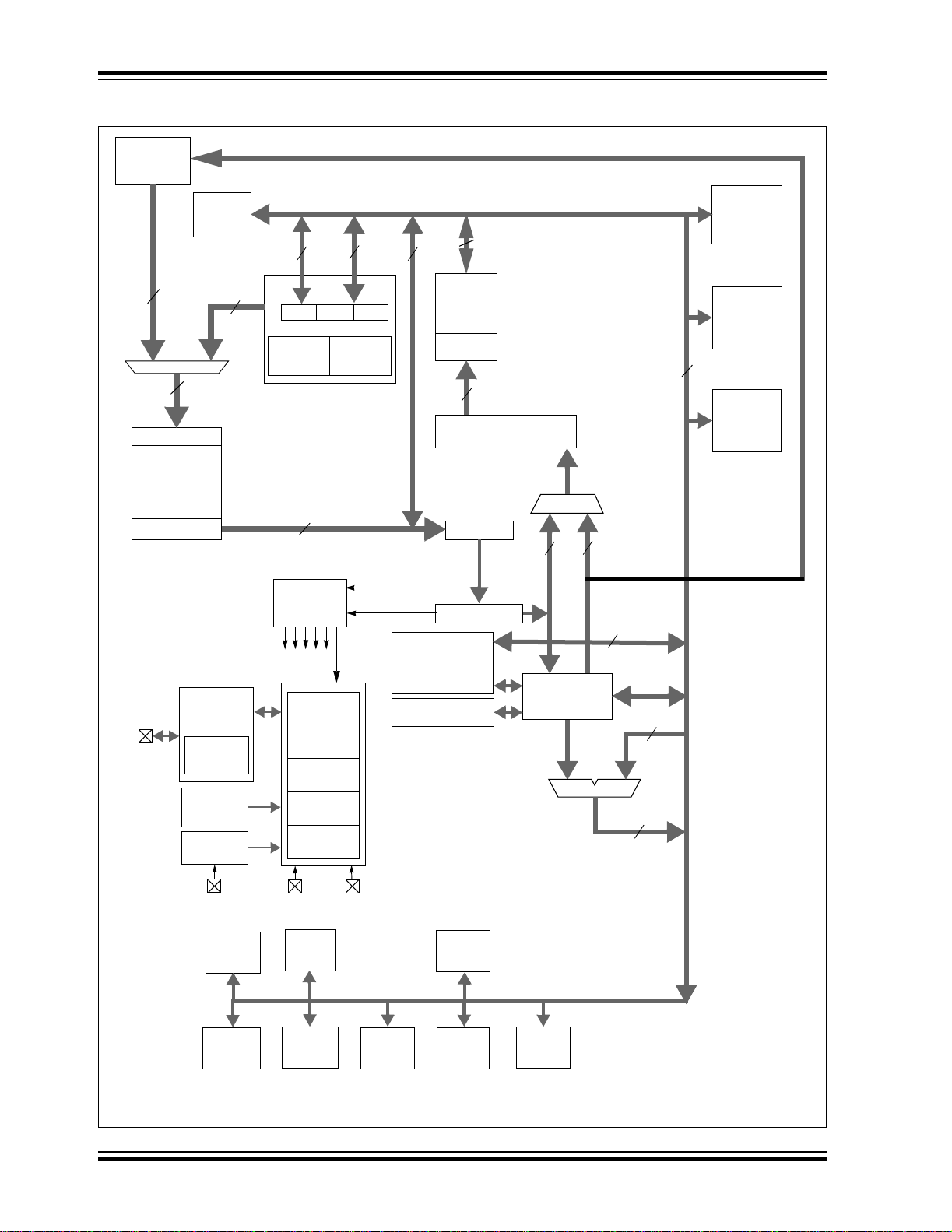
Figure 1-1 shows a general block diagram of the core
and periph eral modules in the PIC24 HJ12GP201/ 202
family of devices. Table 1-1 lists the functions of the
various pins shown in the pinout diagrams.
PIC24HJ12GP201/202
© 2007 Microchip Technology Inc. Advance Information DS70282A-page 7
PIC24HJ12GP201/202
FIGURE 1-1: PIC24HJ12GP201/202 BLOCK DIAGRAM
PSV & Table
Data Access
Control Block
23
Address Latch
Program Memory
Data Latch
OSC2/CLKO
OSC1/CLKI
Interrupt
Controller
23
Timing
Generation
FRC/LPRC
Oscillators
Precision
Band Gap
Reference
Voltage
Regulator
23
Stack
Control
Address Bus
Instruction
Control Signals
to Various Blocks
8
PCH PCL
PCU
Program Counter
Loop
Logic
Control
Logic
24
Decode &
Control
Power-up
Timer
Oscillator
Start-up Timer
Power-on
Reset
Watchdog
Timer
Brown-out
Reset
16
Data Bus
16
Data Latch
X RAM
Address
Latch
16
Address Generator Units
ROM Latch
Instruction Reg
17 x 17 Multiplier
Divide Support
16
W Register Array
EA MUX
16
Literal Data
16 x 16
16-bit ALU
16
16
16
16
16
PORTA
PORTB
Remappable
Pins
VDDCORE/VCAP
Timers
1-3
IC1,2,7,8
DD, VSS
V
PWM1,2
ADC1
OC/
MCLR
CNx
UART1
SPI1
I2C1
Note: Not all pins or features are implemented on all device pinout configurations. See pinout diagrams for the specific pins
and features present on each device.
DS70282A-page 8 Advance Information © 2007 Microchip Technology Inc.

PIC24HJ12GP201/202
TABLE 1-1: PINOUT I/O DESCRIPTIONS
Pin Name Pin Type Buffer Type Description
AN0-AN9 I Analog Analog input channels.
CLKI
CLKO
OSC1
OSC2
SOSCI
SOSCO
CN0-CN7
CN11-CN15
CN21-CN24
CN27
CN29-CN30
IC0-IC1
IC7-IC8
OCFA
OC1-OC2
INT0
INT1
INT2
RA0-RA4 I/O ST PORTA is a bidirectional I/O port.
RB0-RB15 I/O ST PORTB is a bidirectional I/O port.
T1CK
T2CK
T3CK
U1CTS
U1RTS
U1RX
U1TX
SCK1
SDI1
SDO1
SS
1
SCL1
SDA1
ASCL1
ASDA1
TMS
TCK
TDI
TDO
PGD1/EMUD1
PGC1/EMUC1
PGD2/EMUD2
PGC2/EMUC2
PGD3/EMUD3
PGC3/EMUC3
DDCORE P — CPU logic filter capacito r connection.
V
SS P — Ground reference for logic and I/O pins.
V
VREF+ I Analog Analog voltage referenc e (h igh) input.
REF- I Analog Analog voltage reference (low) input.
V
Legend: CMOS = CMOS compatible input or output; Analog = Analog input
ST = Schmitt Trigger input with CMOS levels; O = Output; I = Input; P = Power
I
O
I
I/O
I
O
I ST Change notification inputs.
I ST Capture inputs 1/2
I
O
I
I
I
I
I
I
I
O
I
O
I/O
I
O
I/O
I/O
I/O
I/O
I/O
I
I
I
O
I/O
I
I/O
I
I/O
I
ST/CMOS—External clock source input. Alwa ys associated with OSC1 pin fu nction.
Oscillator crystal output. Connects to crystal or resonator in Crystal Oscillator
mode. Optionally functions as CLKO in RC and EC modes. Always associated
with OSC2 pin function.
ST/CMOS—Oscillator crystal input. ST buffer when configured in RC mode; CMOS otherwise.
ST/CMOS—32.768 kHz low-powe r os ci lla t or cry stal in put; C M O S ot her wi se.
ST
—
ST
ST
ST
ST
ST
ST
ST
—
ST
—
ST
ST
—
ST
ST
ST
ST
ST
ST
ST
ST
—
ST
ST
ST
ST
ST
ST
Oscillator crystal output. Connects to crystal or resonator in Crystal Oscillator
mode. Optionally functio ns as C LKO in R C an d EC m odes.
32.768 kHz low-powe r os ci lla t or cry stal out put.
Can be software programmed for internal weak pull-ups on all inputs.
Capture inputs 7/8
Compare Fault A input (for Compare Channels 1 and 2).
Compare outputs 1 through 2.
External interrupt 0.
External interrupt 1.
External interrupt 2.
Timer1 external clock input.
Timer2 external clock input.
Timer3 external clock input.
UART1 clear to send.
UART1 ready to send.
UART1 receive.
UART1 transmit.
Synchronous serial clock input/output for SPI1.
SPI1 data in.
SPI1 data out.
SPI1 slave synchronization or frame pulse I/O.
Synchronous serial clock input/output for I2C1 .
Synchronous serial data input/output for I2C1.
Alternate synchronous serial clock input/output for I2C1.
Alternate synchronous serial data input/output for I2C1.
JTAG Test mode select pin.
JTAG test clock input pin.
JTAG test data input pin.
JTAG test data output pin.
Data I/O pin for programmin g/ deb ugging communication channel 1.
Clock input pin for progr am m i ng/ d ebugging communica tion channel 1.
Data I/O pin for programmin g/ deb ugging communication channel 2.
Clock input pin for progr am m i ng/ d ebugging communica tion channel 2.
Data I/O pin for programmin g/ deb ugging communication channel 3.
Clock input pin for progr am m i ng/ d ebugging communica tion channel 3.
© 2007 Microchip Technology Inc. Advance Information DS70282A-page 9

PIC24HJ12GP201/202
TABLE 1-1: PINOUT I/O DESCRIPTIONS (CONTINUED)
Pin Name Pin Type Buffer Type Description
AVDD P P Positive supply for analog mo dules.
MCLR
VSS P P Ground refe re nce for analog modules.
A
VDD P — Positive supply for perip her al logi c and I/O pins.
Legend: CMOS = CMOS compatible input or output; Analog = Analog input
ST = Schmitt Trigger input with CMOS levels; O = Output; I = Input; P = Power
I/P ST Master Clear (Reset) input. This pi n is an active-low Reset to the device.
DS70282A-page 10 Advance Information © 2007 Microchip Technology Inc.

PIC24HJ12GP201/202
2.0 CPU
Note: This data sheet summarizes the features
of this group of PIC24HJ12GP201/202
devices. It is not intended to be a comprehensive reference sourc e. To complement
the information in this data sheet, refer to
the “PIC24H Family Reference Manual”.
Please see the Microchip web site
(www.microchip.com) for the latest
PIC24H Family Reference Manual
chapters.
The PIC24HJ12GP201/202 CPU module has a 16-bit
(data) modified H arvard architecture with an enhanced
instruction set and addressing modes. The CPU has a
24-bit instruction word with a variable length opcode
field. The Program Counter (PC) is 23 bits wide and
addresses up to 4M x 24 bits of user program memory
space. The actual amount of program memory
implemented varies by device. A single-cycle
instruction prefetch mechanism is used to help
maintain throughput and provides predictable
execution. All instructions execute in a single cycle,
with the exception of instructions that change the
program flow, the double-word move (MOV.D)
instruction and the table instructions. Overhead-free,
single-cycle program loop constructs are supported
using the REPEAT instructio n, which is in terruptib le at
any point.
The PIC24HJ12GP201/202 devices have sixteen, 16-bit
working regist ers in the program mer’s model. Each of th e
working registers can serve as a data, address or
address offset register. The 16th working register (W15)
operates as a software Stack Pointer (SP) for interrupts
and calls.
The PIC24HJ12GP201/202 instruction set includes
many addressing modes and is designed for optimum
C compiler efficiency. For most instructions, the
PIC24HJ12GP201/202 is capable of executing a data
(or program data) memory read, a working register
(data) read, a data memory write and a program
(instruction) memory read per instruction cycle. As a
result, three parameter instructions can be supported,
allowing A + B = C operations to be executed in a single
cycle.
A block diagram of the CPU is shown in Figure 2-1,
and the programmer’s model for the
PIC24HJ12GP201/202 is sh ow n in Figu re 2-2.
2.1 Data Addressing Overvi ew
The data space can be linearly addressed as 32K words
or 64 Kbytes using an Addr ess Generation Uni t (AGU).
The upper 32 Kby tes of the data s pace mem ory map ca n
optionally b e mapped into pro gram space at any 16K program word boundary defined by the 8-bit Program Space
Visibility Page ( PSVPAG) register. The program to data
space mapping feature lets any instruction access program space as if it were data spac e .
The data space also includes 2 Kbytes of DMA RAM,
which is primarily us ed for DMA dat a transfers, but may
be used as general purpose RAM.
2.2 Special MCU Features
The PIC24HJ12GP201/202 features a 17-bit by 17-bit,
single-cycle multiplier. The multiplier can perform
signed, unsigned and mixed-sign multiplication. Using
a 17-bit by 17-bit multiplier for 16-bit by 16-bit
multiplication makes mixed-sign multiplication
possible.
The PIC24HJ12GP201/202 supports 16/16 and 32/16
integer divide operations. All divide instructions are
iterative operations. They must be executed within a
REPEAT loop, resulting in a total execution time of 19
instruction cycles. The divide operation can be
interrupted during any of those 19 cycles without loss
of data.
A multi-bit data shifter is used to perform up to a 16-bit,
left or right shift in a single cycle.
© 2007 Microchip Technology Inc. Advance Information DS70282A-page 11
PIC24HJ12GP201/202
FIGURE 2-1: PIC24HJ12GP201/202 CPU CORE BLOCK DIAGRAM
PSV & Table
Data Access
Control Block
Interrupt
Controller
23
23
Address Latch
Program Memory
Data Latch
23
8
PCH PCL
PCU
Program Counter
Stack
Control
Logic
Address Bus
24
Instruction
Decode &
Control
Control Signals
to Various Blocks
16
Loop
Control
Logic
X Data Bus
16
Data Latch
X RAM
Address
Latch
Address Generator Units
ROM Latch
Instruction Reg
17 x 17
Multiplier
Divide Support
16
16
EA MUX
16
16
Literal Data
16 x 16
W Register Array
16
16
16
16-bit ALU
16
To Peripheral Modules
DS70282A-page 12 Advance Information © 2007 Microchip Technology Inc.
PIC24HJ12GP201/202
FIGURE 2-2: PIC24HJ12GP201/202 PROGRAMMER’S MODEL
D0D15
W0/WREG
W1
W2
W3
W4
W5
W6
W7
W8
W9
W10
W11
W12
W13
W14/Frame Pointer
W15/Stack Pointer
PUSH.S Shadow
DO Shadow
Legend
Working Registers
PC22
7
TBLPAG
7
PSVPAG
— — ——
SRH
0
0
— —
SPLIM Stack Pointer Limit Register
Data Table Page Address
Program Space Visibility Page Address
15
RCOUNT
15
CORCON
— DC
IPL2 IPL1
IPL0 OV
RA N
SRL
PC0
0
Program Counter
0
REPEAT Loop Counter
0
Core Configuration Register
C
Z
STATUS Register
© 2007 Microchip Technology Inc. Advance Information DS70282A-page 13
PIC24HJ12GP201/202
2.3 CPU Control Registers
REGISTER 2-1: SR: CPU STATUS REGISTER
U-0 U-0 U-0 U-0 U-0 U-0 U-0 R/W-0
— — — — — — —DC
bit 15 bit 8
(1)
R/W-0
IPL<2:0>
bit 7 bit 0
Legend:
C = Clear only bit R = Readable bit U = Unimplemented bit, read as ‘0’
S = Set only bit W = Writable bit -n = Value at POR
‘1’ = Bit is set ‘0’ = Bit is cleared x = Bit is unknown
bit 15-9 Unimplemented: Read as ‘0’
bit 8 DC: MCU ALU Half Carry/Borrow
1 = A carry-out from the 4th low-order bit (for byte-si zed data) or 8th lo w-order bit (for word-s ized data)
0 = No carry-out from the 4th low-order bit (for byte-sized data) or 8th low-order bit (for word-sized
bit 7-5 IPL<2:0>: CPU Interrupt Priority Level Status bits
111 = CPU Interrupt Priority Level is 7 (15), user interrupts disabled
110 = CPU Interrupt Priority Level is 6 (14)
101 = CPU Interrupt Priority Level is 5 (13)
100 = CPU Interrupt Priority Level is 4 (12)
011 = CPU Interrupt Priority Level is 3 (11)
010 = CPU Interrupt Priority Level is 2 (10)
001 = CPU Interrupt Priority Level is 1 (9)
000 = CPU Interrupt Priority Level is 0 (8)
bit 4 RA: REPEAT Loop Active bit
1 = REPEAT loop in progress
0 = REPEAT loop not in progress
bit 3 N: MCU ALU Negative bit
1 = Result was negative
0 = Result was non-negative (zero or positive)
bit 2 OV: MCU ALU Overflow bit
This bit is used for signed arithm etic (2’s c omplement). It indic ates an overflow of th e magnitude wh ich
causes the sign bit to change state.
1 = Overflow occurred for signed arithmetic (in this arithmetic operation)
0 = No overflow occurred
bit 1 Z: MCU ALU Zero bit
1 = An operation which affects the Z bit has set it at some time in the past
0 = The most recent operation which affects the Z bit has cleared it (i.e., a non-zero result)
bit 0 C: MCU ALU Carry/Borrow
1 = A carry-out from the Most Significant bit (MSb) of the result occurred
0 = No carry-out from the Most Significant bit of the result occurred
Note 1: The IPL<2:0> bits are concaten ated with the IPL<3 > bi t (CORCON<3 >) to form the CPU Inte rrup t Prio rity
Level. The value in parentheses indicates the IPL if IPL<3> = 1. User interrupts are disabled when
IPL<3> = 1.
2: The IPL<2:0> Status bits are read only when NSTDIS = 1 (INTCON1<15>).
(2)
R/W-0
(2)
of the result occurred
data) of the result occurred
R/W-0
(2)
R-0 R/W-0 R/W-0 R/W-0 R/W-0
RA N OV Z C
bit
(2)
bit
DS70282A-page 14 Advance Information © 2007 Microchip Technology Inc.

PIC24HJ12GP201/202
REGISTER 2-2: CORCON: CORE CONTROL REGISTER
U-0 U-0 U-0 U-0 U-0 U-0 U-0 U-0
— — — — — — — —
bit 15 bit 8
U-0 U-0 U-0 U-0 R/C-0 R/W-0 U-0 U-0
— — — —IPL3
bit 7 bit 0
Legend: C = Clear only bit
R = Readable bit W = Writable bit -n = Value at POR ‘1’ = Bit is set
0’ = Bit is cleared ‘x = Bit is unknown U = Unimplemented bit, read as ‘0’
bit 15-4 Unimplemented: Read as ‘0’
bit 3 IPL3: CPU Interrupt Priority Level Status bit 3
1 = CPU interrupt priority level is greater than 7
0 = CPU interrupt priori ty level is 7 o r less
bit 2 PSV: Program Space Visibility in Data Space Enable bit
1 = Program space visible in data space
0 = Program space not visible in data space
bit 1-0 Unimplemented: Read as ‘0’
Note 1: The IPL3 bit is concatenated with the IPL<2:0> bits (SR<7:5>) to form the CPU interrupt priority level.
(1)
(1)
PSV — —
© 2007 Microchip Technology Inc. Advance Information DS70282A-page 15

PIC24HJ12GP201/202
2.4 Arithmetic Logic Unit (ALU)
The PIC24HJ12GP201/202 ALU is 16 bits wide and is
capable of addition, subtraction, bit shifts and logic
operations. Unless otherwise mentioned, arithmetic
operations are 2’s complement in nature. Depending
on the operation, the ALU may affect the values of the
Carry (C), Zero (Z), Negative (N), Overflow (OV) and
Digit Carry (DC) Status bits in the SR register. The C
and DC S tatus bits op erate as Bo rrow
bits, respectively, for subtraction operations.
The ALU can perform 8-bit or 16-bit operations,
depending on the mode of the instruction that is used.
Data for the ALU operation can come from the W register array , or dat a memory, depending on the addressing mode of the instruction. Likewise, output data from
the ALU can be written to the W regis ter array or a data
memory locatio n.
Refer to the “dsPIC30F/33F Programmer’s Reference
Manual” (DS70157) for information on the SR bits
affected by each instruction.
The PIC24HJ12GP201/202 CPU incorporates hardware support for both multiplication and division. This
includes a dedicated hardware multiplier and support
hardware for 16-bit divisor division.
2.4.1 MULTIPLIER
Using the high-speed 17-bit x 17-bit multiplier, the ALU
supports unsigned, signed or mixed-sign operation in
several multiplication modes:
1. 16-bit x 16-bit signed
2. 16-bit x 16-bit unsigned
3. 16-bit signed x 5-bit (literal) unsigned
4. 16-bit unsigned x 16-bit unsigned
5. 16-bit unsigned x 5-bit (literal) unsigned
6. 16-bit unsigned x 16-bit signed
7. 8-bit unsigned x 8-bit unsigned
and Digit Borrow
2.4.2 DIVIDER
The divide block support s 32-bit/16-bit and 16-b it/16-bit
signed and unsig ne d in teg er d iv ide ope rati on s w it h th e
following data si zes:
1. 32-bit signed/16-bit signed divide
2. 32-bit unsigned/16-bit unsigned divide
3. 16-bit signed/16-bit signed divide
4. 16-bit unsigned/16-bit unsigned divide
The quotient for all divide instructions ends up in W0
and the remainder in W1. Sixteen-bit signed and
unsigned DIV instructions can specify any W register
for both the 16-bit divisor (Wn) and any W register
(aligned) pair (W(m + 1):Wm) for the 32-bit dividend.
The divide algorithm takes one cycle per bit of divisor,
so both 32-bit/16-bit and 16-bit/16-bit instructions take
the same number of cycles to execute.
2.4.3 MULTI-BIT DATA SHIFTER
The multi-bit data shifter is capable of performing up to
16-bit arithmetic or logic right shifts , or up to 16-bit left
shifts in a single cycle. The source can be either a
working register or a memory location.
The shifter requi res a signed binary value to determine
both the magnitude (num ber of bits) and direction of the
shift operation. A po sitive value shif ts the operand right.
A negative value shifts the operand left. A value of ‘0’
does not modify the operand.
DS70282A-page 16 Advance Information © 2007 Microchip Technology Inc.
PIC24HJ12GP201/202
3.0 MEMORY ORGANIZATION
Note: This data sheet summarizes the features
of the PIC24HJ 12GP201/202 d evices. It is
not intended to be a c om preh ens iv e re ference source. To complement the information in this data sheet, refer to the “PIC24H
Family Reference Manual”. Please see
the Microchip web site (www.microchip.com) for the latest PIC24H Family
Reference Manual chapters.
The PIC24HJ12GP201/202 architecture features separate program and data memory spaces and buses.
This architecture also allows the direct access of program memory from the data space during code execution.
3.1 Program Address Space
The program address memory space of the
PIC24HJ12GP201/202 devices is 4M instructions. The
space is addressable by a 24-bit value derived either from
the 23-bit Program Counter (PC) during program execution, or from table operation or data space remapping as
described in Section 3.4 “Interfacing Program and Data
Memory Spaces”.
User application a ccess t o the pr ogram me mory s pace is
restricted to the lower half of the address range (0x000000
to 0x7FFFFF). The exception is the use of TBLRD/TBLWT
operations, which use TBLPAG<7> to permit access to the
Configura tion bi ts an d Devic e ID sect ions of the
configuration memory space.
The memory map for the PIC24HJ12GP201/202 device is
shown in Figu re3-1.
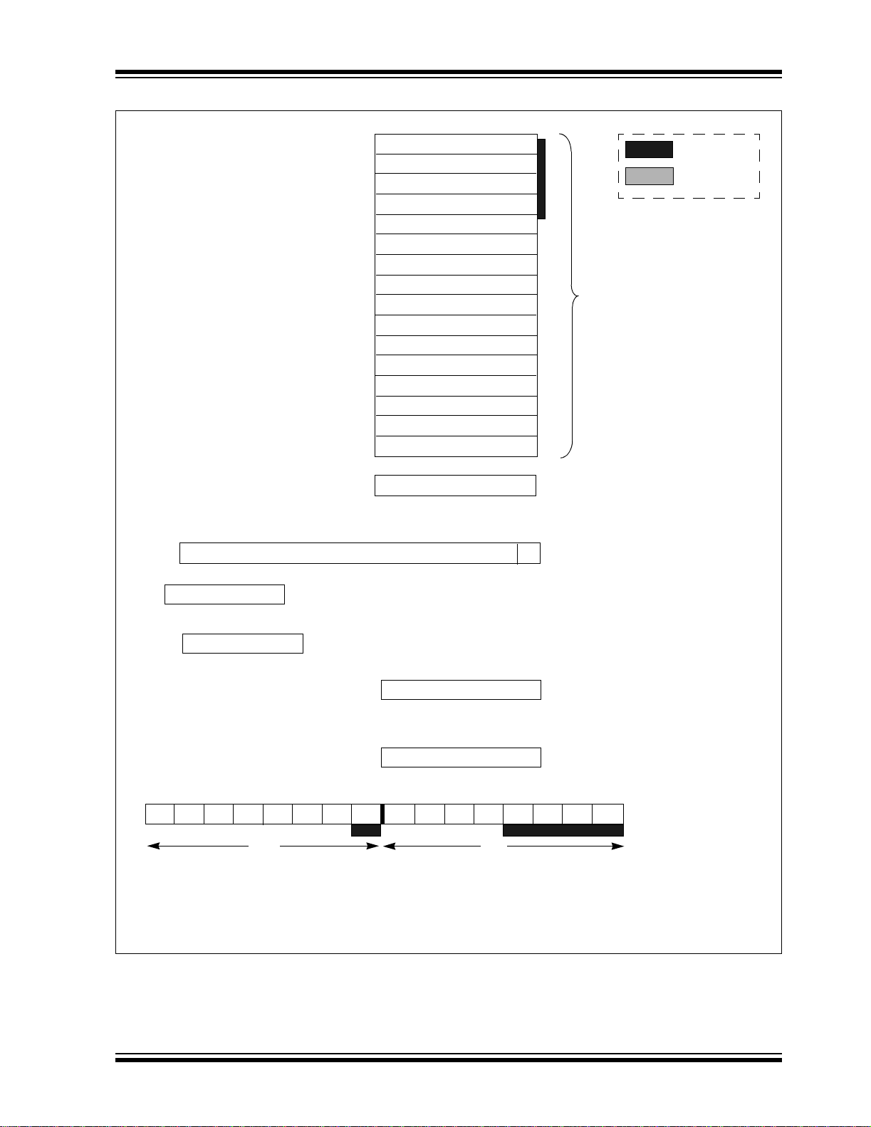
FIGURE 3-1: PROGRAM MEMORY FOR PIC24HJ12GP201/202 DEVICES
PIC24HJ12GP201/202
GOTO
Instruction
Reset Address
Interrupt Vector Table
Reserved
Alternate Vector Table
User Program
Flash Memory
(4K instructions)
0x000000
0x000002
0x000004
0x0000FE
0x000100
0x000104
0x0001FE
0x000200
0x001FFE
0x002000
User Memory Space
Unimplemented
Device Configuration
Configuration Memory Space
(Read ‘0’s)
Reserved
Registers
Reserved
DEVID (2)
0x7FFFFE
0x800000
0xF7FFFE
0xF80000
0xF80017
0xF80018
0xFEFFFE
0xFF0000
0xFFFFFE
© 2007 Microchip Technology Inc. Advance Information DS70282A-page 17
PIC24HJ12GP201/202
3.1.1 PROGRAM MEMORY
ORGANIZATION
The program memory space is organized in wordaddressable blocks. Although it is treated as 24 bits
wide, it is more appropriate to think of each address of
the program memory as a lower and upper word, with
the upper byte of t he upper word being unimplemented.
The lower word always has an even address, while the
upper word has an odd address (Figure 3-2).
Program memory addresses are always word-aligned
on the lower word, and addresses are incremented or
decremented by two during code execution. This
arrangement provides compatibility with data memory
space addressing and makes data in the program
memory space accessible.
3.1.2 INTERRUPT AND TRAP VECTORS
All PIC24HJ12GP201/202 devices reserve the
addresses between 0x00000 and 0x000200 for hardcoded program execution vectors. A hardware Reset
vector is provided to redirect code execution from the
default value of the PC on device Reset to the actual
start of code. A GOTO in stru ction is programmed by the
user application at 0x000000, with the actual address
for the start of code at 0x000002.
PIC24HJ12GP201/202 devic es al so ha ve tw o in terrupt
vector tables, lo cated from 0x 00000 4 to 0x 0000F F and
0x000100 to 0x0001FF. These vector tab les allow each
of the many device interrupt sources to be handled by
separate Interrupt Service Routines (ISRs). A more
detailed discussion of the interrupt vector tables is
provided in Section6.1 “Interrupt Vector Table”.
FIGURE 3-2: PROGRAM MEMORY ORGANIZATION
msw
Address (lsw Address)
0x000001
0x000003
0x000005
0x000007
most significant word
23
00000000
00000000
00000000
00000000
least significant word
PC Address
0816
0x000000
0x000002
0x000004
0x000006
Program Memor y
‘Phantom’ Byte
(read as ‘0’)
Instructi on Width
DS70282A-page 18 Advance Information © 2007 Microchip Technology Inc.

PIC24HJ12GP201/202
3.2 Data Address Space
The PIC24HJ12GP201/202 CPU has a separate 16bit-wide data memory space. The data space is
accessed using separate Address Generation Units
(AGUs) for read and write operations. The data
memory maps is shown in Figure 3-3.
All Effective Addresses (EAs) in the data memory space
are 16 bits wide and point to bytes within the data space.
This arrangement gives a data space address range of
64 Kbytes or 32K words. The lower half of the data
memory space (that is, when EA<15> = 0) is used for
implemented memory addresses, while the upper half
(EA<15> = 1) is reserved for the Program Space
Visibility area (see Section 3.4.3 “Reading D ata From
Program Memory Using Program Space Visibility”).
PIC24HJ12GP201/202 devices implement up to
30 Kbytes o f data memory. Should an EA poi nt to a
location outside of this area, an all-zero word or byte
will be returned.
3.2.1 DATA SPACE WIDTH
The data memory space is organized in byte addressable, 16-bit-wide blocks. Data is aligned in data
memory and registers as 16-bit words, but all data
space EAs resolve to bytes. The Least Significant
Bytes (LSBs) of each word have even ad dresses, whil e
the Most Significant Bytes (MSBs) have odd
addresses.
3.2.2 DATA MEMORY ORGANIZATION
AND ALIGNMENT
To ma intain backwa rd compatibili ty with PIC
and improve data space memory usage efficiency, the
PIC24HJ12GP201/202 instruction set supports both
word and byte operations. As a consequence of byte
accessibility , a ll effect ive address calcu lations are internally scaled to step through word-aligned memory. For
example, the core recognizes that Post-Modified
Register Indirect Addre ssing mode [Ws++] w ill resu lt in
a value of W s + 1 for by te operat ions and Ws + 2 for
word operations.
Data byte reads will read the complete word that
contains the byte, using the LSB of any EA to determine which byte to select. The selected byte is placed
onto the LSB of the data path. That is, data memory
and registers are organized as two parallel byte-wide
entities with shared (word) address decode but separate write lines. D at a by te writ es only wri te to t he co rresponding side of the array or register that matches the
byte address.
®
devices
All word accesses m ust be al igned to an even addre ss.
Misaligned word data fetches are not supported, so
care must be taken when mixing byte and word operations, or translating from 8-bit MCU code. If a misaligned read or write is attempted, an address error
trap is generated. If the error occurred on a read, the
instruction underway is completed. If the instruction
occurred on a write, the instruction is executed but the
write does not occur. In either case, a trap is then executed, allowing the system and/or user application to
examine the machine state prior to execution of the
address Fault.
All byte loads into any W register are loaded into the
Least Significant Byte. The Most Significant Byte is n ot
modified.
A sign-extend instruction (SE) is provided to allow
users to translate 8-bit signed data to 16-bit signed
values. Alternatively, for 16-bit unsigned data, user
applications can clear the MSB of any W register by
executing a zero-extend (ZE) instruction on the
appropriate address.
3.2.3 SF R SPAC E
The first 2 Kbytes of the near data space, from 0x0000
to 0x07FF, is primarily occupied by Special Function
Registers (SFRs). These are used by the
PIC24HJ12GP201/202 core and peripheral modules
for controlling the operation of the device.
SFRs are distributed among the modules that they
control, and are generall y grouped together by mod ule.
Much of the SFR space contains unused addresses;
these are read as ‘0’. A co mplete listing o f implemented
SFRs, including their addresses, is shown in Table 3-1
through Table 3-21.
Note: The actual set of peripheral features and
interrupts varies by the device. Refer to
the corresponding device tables and
pinout diagrams for device-specific
information.
3.2.4 NEAR DATA SPACE
The 8 Kbyte area between 0x0000 and 0x1FFF is
referred to as t he near data space. Locations in this
space are directly addressable via a 13-bit absolute
address field within all memory direct instructions.
Additionally, the whole data spa ce is addressa ble using
MOV instructions, which support Memory Direct
Addressing mode with a 16-bit address field, or by
using Indirect Addressing mode using a working
register as an address pointer.
© 2007 Microchip Technology Inc. Advance Information DS70282A-page 19
PIC24HJ12GP201/202
e
FIGURE 3-3: DATA MEMORY MAP FOR PIC24HJ12GP201/202 DEVICES WITH 1 KB RAM
2 Kbyte
SFR Space
1 Kbyte
SRAM Space
MSB
Address
0x0001
0x07FF
0x0801
0x0BFF
0x0C01
0x1FFF
0x2001
0x8001
16 bits
SFR Space
X Data RAM (X)
LSB
Address
LSbMSb
0x0000
0x07FE
0x0800
8 Kbyte
Near Data Spac
0x0BFE
0x0C00
0x1FFFF
0x2000
0x8000
Optionally
Mapped
into Program
Memory
0xFFFF
X Data
Unimplemented (X)
0xFFFE
DS70282A-page 20 Advance Information © 2007 Microchip Technology Inc.
© 2007 Microchip Technology Inc. Advance Information DS70282A-page 21
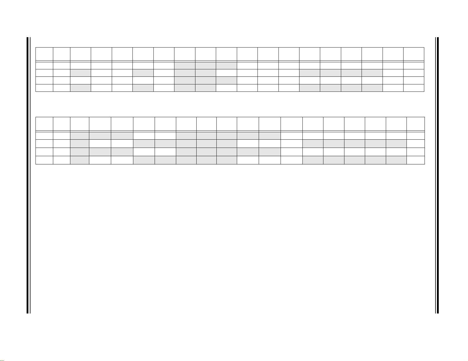
TABLE 3-1: CPU CORE REGISTERS MAP
SFR Name
WREG0 0000 Working Re gis ter 0
WREG1 0002 Working Re gis ter 1
WREG2 0004 Working Re gis ter 2
WREG3 0006 Working Re gis ter 3
WREG4 0008 Working Re gis ter 4
WREG5 000A Working Re gis ter 5
WREG6 000C Wo rkin g Re gis ter 6
WREG7 000E Working Re gis ter 7
WREG8 0010 Working Re gis ter 8
WREG9 0012 Working Re gis ter 9
WREG10 0014 Working Register 10
WREG11 0016 Working Register 11
WREG12 0018 Working Register 12
WREG13 001A Working Register 13
WREG14 001C Working Register 14
WREG15 001E Working Register 15
SPLIM 0020 Stack Pointer Limit Register
PCL 002E Program Counter Low Word Register
PCH 0030 — — — — — — — — Program C ounte r Hi gh B yte Re gi ster
TBLP A G 0032 — — — — — — — — Table Page Address Pointer R egis ter
PSVPAG 0034 — — — — — — — — Program Memory Visibility Page Address Pointer Register
RCOUNT 0036 Repeat Loop Counter Register
SR 0042 — — — — — — — DC IPL2 IPL1 IPL0 RA N OV Z C
CORCON 0044 — — — — — — — — — — — —
DISICNT 0052 —
Legend: x = unknown value on Reset, — = unimplemented, read as ‘0’. Reset values are shown in hexadecimal.
SFR
Addr
Bit 15 Bit 14 Bit 13 Bit 12 Bit 11 Bit 10 Bit 9 Bit 8 Bit 7 Bit 6 Bit 5 Bit 4 Bit 3 Bit 2 Bit 1 Bit 0
— Disable Interrupts Counter
IPL3 PSV
Register
— —
All
Resets
0000
0000
0000
0000
0000
0000
0000
0000
0000
0000
0000
0000
0000
0000
0000
0800
xxxx
0000
0000
0000
0000
xxxx
0000
0000
xxxx
PIC24HJ12GP201/202
DS70282A-page 22 Advance Information © 2007 Microchip Technology Inc.
TABLE 3-2: CHANGE NOTIFICATION REGISTER MAP FOR PIC24HJ12GP202
SFR
SFR
Name
CNEN1 0060 CN15IE CN14IE CN13IE CN12IE CN11IE
CNEN2 0062
CNPU1 0068 CN15PUE CN14PUE CN13PUE CN1 2PUE CN1 1PUE
CNPU2 006A
Legend: x = unknown value on Reset, — = unimplemented, read as ‘0’. Reset values are shown in hexadecimal.
Addr
Bit 15 Bit 14 Bit 13 Bit 12 Bit 11 Bit 10 Bit 9 Bit 8 Bit 7 Bit 6 Bit 5 Bit 4 Bit 3 Bit 2 Bit 1 Bit 0
—- — —
CN30IE CN29IE
—
CN30PUE CN29PUE
—
CN27IE
—
CN27PUE
—
— —
— — —
— —
CN24PUE CN23IE CN22IE CN21IE
CN24PUE CN23PUE CN22PUE CN21PUE
TABLE 3-3: CHANGE NOTIFICATION REGISTER MAP FOR PIC24HJ12GP201
SFR
SFR
Name
CNEN1 0060
CNEN2 00C2
CNPU1 0068
CNPU2 006A
Legend: x = unknown value on Reset, — = unimplemented, read as ‘0’. Reset values are shown in hexadecimal.
Bit 15 Bit 14 Bit 13 Bit 12 Bit 11 Bit 10 Bit 9 Bit 8 Bit 7 Bit 6 Bit 5 Bit 4 Bit 3 Bit 2 Bit 1 Bit 0
Addr
— — —
—
CN30IE CN29IE
— — —
—
CN30PUE CN29PUE
CN12IE CN11IE
— — — — —
CN12PUE CN11PUE
— — — — —
— — — — —
— — — — —
CN7IE CN6IE CN5IE CN4IE CN3IE CN2IE CN1IE CN0IE
— — — —
CN7PUE CN6PUE CN5PUE CN4PUE CN3PUE CN2PUE CN1PUE CN0PUE
— — — —
CN5IE CN4IE CN3IE CN2IE CN1IE CN0IE 0000
CN23IE CN22IE CN21IE
CN5PUE CN4PUE CN3PUE CN2PUE CN1PUE CN0PUE 0000
CN23PUE CN22PUE CN21PUE
— — — — —
— — — — —
CN16IE
CN16PUE
PIC24HJ12GP201/202
All
Resets
0000
0000
0000
0000
All
Resets
0000
0000
© 2007 Microchip Technology Inc. Advance Information DS70282A-page 23
TABLE 3-4: INTERRUPT CONTROLLER REGISTER MAP
SFR
Name
INTCON1 0080 NSTDIS
INTCON2 0082 ALTIVT DISI
IFS0 0084
IFS1 0086
IFS4 008C
IEC0 0094
IEC1 0096
IEC4 009C
IPC0 00A4
IPC1 00A6
IPC2 00A8
IPC3 00AA
IPC4 00AC
IPC5 00AE
IPC7 00B2
IPC16 00C4
INTTREG 00E0
Legend: x = unknown value on Reset, — = unimplemented, read as ‘0’. Reset values are shown in hexadecimal.
SFR
Bit 15 Bit 14 Bit 13 Bit 12 Bit 11 Bit 10 Bit 9 Bit 8 Bit 7 Bit 6 Bit 5 Bit 4 Bit 3 Bit 2 Bit 1 Bit 0
Addr
— — — — — — — —
— — — — — — — — — — — INT2EP INT1EP INT0EP 0000
— — AD1IF U1TXIF U1RXIF SPI1IF SPI1EIF T3IF T2IF OC2IF IC2IF — T1IF OC1IF IC1IF INT0IF 0000
— —INT2IF — — — — — IC8IF IC7IF — INT1IF CNIF — MI2C1IF SI2C1IF 0000
— — — — — — — — — — — — — —U1EIF— 0000
— — AD1IE U1TXIE U1RXIE SPI1IE SPI1EIE T3IE T2IE OC2IE IC2IE — T1IE OC1IE IC1IE INT0IE 0000
— —INT2IE — — — — — IC8IE IC7IE — INT1IE CNIE — MI2C1IE SI2C1IE 0000
— — — — — — — — — — — — — —U1EIE— 0000
— T1IP<2:0> —OC1IP<2:0>—IC1IP<2:0>— INT0IP<2:0> 4444
— T2IP<2:0> —OC2IP<2:0>—IC2IP<2:0>— — — — 4444
— U1RXIP<2:0> — SPI1IP<2:0> — SPI1EIP<2:0> — T3IP<2:0> 4444
— — — — — — — — — AD1IP<2:0> — U1TXIP<2:0> 4444
— CNIP<2:0> — — — — — MI2C1IP<2:0> — SI2C1IP<2:0> 4444
— IC8IP<2:0> —IC7IP<2:0>— — — — — INT1IP<2:0> 4444
— — — — — — — — — INT2IP<2:0> — — — — 4444
— — — — — — — — — U1EIP<2:0> — — — — 4444
— — — — ILR<3:0>> — VECNUM<6:0> 4444
DIV0ERR
All
Resets
— MATHERR ADDRERR STKERR OSCFAIL — 0000
PIC24HJ12GP201/202
DS70282A-page 24 Advance Information © 2007 Microchip Technology Inc.
PIC24HJ12GP201/202
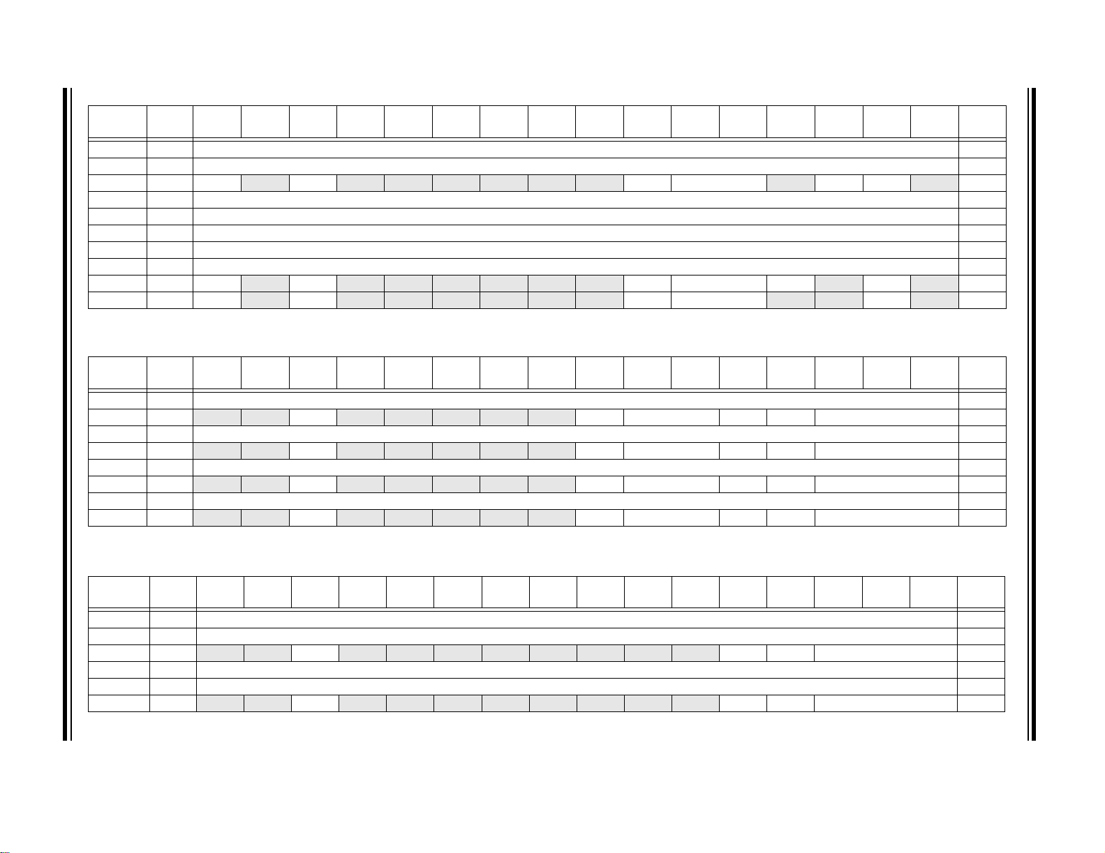
TA BLE 3-5: TIMER REGISTER MAP
SFR Name
TMR1 0100 Timer1 Register
PR1 0102 Period Register 1
T1CON 0104 TON
TMR2 0106 Timer2 Register
TMR3HLD 0108 Timer3 Holding Register (for 32-bit timer operations only)
TMR3 010A Timer3 Register
PR2 010C Period Register 2
PR3 010E Period Register 3
T2CON 0110 TON
T3CON 0112 TON
Legend: x = unknown value on Reset, — = unimplemented, read as ‘0’. Reset values are shown in hexadecimal.
SFR
Addr
Bit 15 Bit 14 Bit 13 Bit 12 Bit 11 Bit 10 Bit 9 Bit 8 Bit 7 Bit 6 Bit 5 Bit 4 Bit 3 Bit 2 Bit 1 Bit 0
—
TSIDL
—
TSIDL
—
TSIDL
— — — — — —
— — — — — —
— — — — — —
TGATE TCKPS<1:0>
TGATE TCKPS<1:0> T32
TGATE TCKPS<1:0>
—
— —
TSYNC TCS
—
TCS
TCS
—
—
—
All
Resets
xxxx
FFFF
0000
xxxx
xxxx
xxxx
FFFF
FFFF
0000
0000
TABLE 3-6: INPUT CAPTURE REGISTER MAP
SFR Name
IC1BUF 0140 Input 1 Capture Register
IC1CON 0142
IC2BUF 0144 Input 2 Capture Register
IC2CON 0146
IC7BUF 0158 Input 7 Capture Register
IC7CON 015A
IC8BUF 015C Input 8C ap tu re R eg iste r
IC8CON 015E
Legend: x = unknown value on Reset, — = unimplemented, read as ‘0’. Reset values are shown in hexadecimal.
SFR
Addr
Bit 15 Bit 14 Bit 13 Bit 12 Bit 11 Bit 10 Bit 9 Bit 8 Bit 7 Bit 6 Bit 5 Bit 4 Bit 3 Bit 2 Bit 1 Bit 0
— —
— —
— —
— —
ICSIDL
ICSIDL
ICSIDL
ICSIDL
— — — — —
— — — — —
— — — — —
— — — — —
ICTMR ICI<1:0> ICOV ICBNE ICM<2:0>
ICTMR ICI<1:0> ICOV ICBNE ICM<2:0>
ICTMR ICI<1:0> ICOV ICBNE ICM<2:0>
ICTMR ICI<1:0> ICOV ICBNE ICM<2:0>
All
Resets
xxxx
0000
xxxx
0000
xxxx
0000
xxxx
0000
TABLE 3-7: OUTPUT COMPARE REGISTER MAP
SFR Name
OC1RS 0180 Output Comp ar e 1 S ec ond ary Reg iste r
OC1R 0182 Output Compare 1 Register
OC1CON 0184
OC2RS 0186 Output Comp ar e 2 S ec ond ary Reg iste r
OC2R 0188 Output Compare 2 Register
OC2CON 018A
Legend: x = unknown value on Reset, — = unimplemented, read as ‘0’. Reset values are shown in hexadecimal.
SFR
Addr
Bit 15 Bit 14 Bit 13 Bit 12 Bit 11 Bit 10 Bit 9 Bit 8 Bit 7 Bit 6 Bit 5 Bit 4 Bit 3 Bit 2 Bit 1 Bit 0
— —
— —
OCSIDL
OCSIDL
— — — — — — — —
— — — — — — — —
OCFLT OCTSEL OCM<2:0>
OCFLT OCTSEL OCM<2:0>
All
Resets
xxxx
xxxx
0000
xxxx
xxxx
0000

© 2007 Microchip Technology Inc. Advance Information DS70282A-page 25
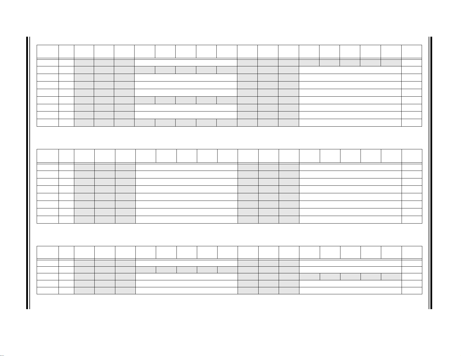
TABLE 3-8: I2C1 REGISTER MAP
SFR Name
I2C1RCV 0200 — — — — — — — — Receive Register
I2C1 T R N 0202 — — — — — — — — Transmi t Re gister
I2C1BRG 0204 — — — — — — — Baud Rate Generat or Regis ter
I2C1CON 0206 I2CEN — I2CSIDL SCLREL IPMIEN A10M DISSLW SMEN GCEN STREN ACKDT ACKEN RCEN PEN RSEN SEN
I2C1STAT 0208 ACKSTA T TRSTAT — — — BCL GCSTAT ADD10 IWCOL I2COV D_A P S R_W RBF TBF
I2C1ADD 020A — — — — — — Address Register
I2C1MSK 020C — — — — — — Address Mask Re gist er
Legend: x = unknown value on Reset, — = unimplemented, read as ‘0’. Reset values are shown in hexadecimal.
SFR
Addr
Bit 15 Bit 14 Bit 13 Bit 12 Bit 11 Bit 10 Bit 9 Bit 8 Bit 7 Bit 6 Bit 5 Bit 4 Bit 3 Bit 2 Bit 1 Bit 0
TABLE 3-9: UART1 REGISTER MAP
SFR Name
U1MODE 0220 UARTEN — USIDL IREN RTSMD — UEN1 UEN0 WAKE LPBACK ABAUD URXINV BRGH PDSEL<1:0> STSEL
U1STA 0222 UTXISEL1 UTXINV UTXISEL0 — UTXBRK UTXEN UTXBF TRMT URXISEL<1:0> ADDEN RIDLE PERR FERR OERR URXDA
U1TXREG 0224 — — — — — — — UART T r an smit R e gister
U1RXREG 0226 — — — — — — — UART Receive Re gister
U1BRG 0228 Baud Ra te G en era to r P r es ca le r
Legend: x = unknown value on Reset, — = unimplemented, read as ‘0’. Reset values are shown in hexadecimal.
SFR
Addr
Bit 15 Bit 14 Bit 13 Bit 12 Bit 11 Bit 10 Bit 9 Bit 8 Bit 7 Bit 6 Bit 5 Bit 4 Bit 3 Bit 2 Bit 1 Bit 0
TABLE 3-10: SPI1 REGISTER MAP
SFR
Name
SPI1STAT 0240 SPIEN — SPISIDL — — — — — — SPIROV — — — — SPITBF SPIRBF
SPI1CON1 0242 — — — DISSCK DISSDO MODE16 SMP CKE SSEN CKP MSTEN SPRE<2:0> PPRE<1:0>
SPI1CON2 0244 FRMEN SPIFSD FRMPOL — — — — — — — — — — — FRMDLY —
SPI1BUF 0248 SPI1 Transmit and Receive Buffer Register
Legend: x = unknown value on Reset, — = unimplemented, read as ‘0’. Reset values are shown in hexadecimal.
SFR
Bit 15 Bit 14 Bit 13 Bit 12 Bit 11 Bit 10 Bit 9 Bit 8 Bit 7 Bit 6 Bit 5 Bit 4 Bit 3 Bit 2 Bit 1 Bit 0
Addr
All
Resets
0000
00FF
0000
1000
0000
0000
0000
All
Resets
0000
0110
xxxx
0000
0000
All
Resets
0000
0000
0000
0000
PIC24HJ12GP201/202
DS70282A-page 26 Advance Information © 2007 Microchip Technology Inc.
TABLE 3-11: PERIPHERAL PIN SELECT INPUT REGISTER MAP
File
Name
RPINR0 0680
RPINR1 0682
RPINR3 0686
RPINR7 068E
RPINR10 0694
RPINR11 0696
RPINR18 06A4
RPINR20 06A8
RPINR21 06AA
Legend: x = unknown value on Reset, — = unimplemented, read as ‘0’. Reset values are shown in hexadecimal.
Addr Bit 15 Bit 14 Bit 13 Bit 12 Bit 11 Bit 10 Bit 9 Bit 8 Bit 7 Bit 6 Bit 5 Bit 4 Bit 3 Bit 2 Bit 1 Bit 0
— — — INT1R<4:0> — — — — — — — —
— — — — — — — — — — —INT2R<4:0>
— — —T3CKR<4:0>— — —T2CKR<4:0>
— — — IC2R<4:0> — — — IC1R<4:0>
— — — IC8R<4:0> — — — IC7R<4:0>
— — — — — — — — — — —OCFAR<4:0>
— — — U1CTSR<4:0> — — —U1RX<R4:0>
— — —SCK1R<4:0>— — —SDI1R<4:0>
— — — — — — — — — — —SS1R<4:0>
All
Resets
1F00
001F
1F1F
1F1F
1F1F
001F
1F1F
1F1F
001F
PIC24HJ12GP201/202
TABLE 3-12: PERIPHERAL PIN SELECT OUTPUT REGISTER MAP FOR PIC24HJ12GP202
File
Name
RPOR0 06C0 — — — RP1R<4:0> — — — RP0R<4:0>
RPOR1 0 6C2
RPOR2 0 6C4
RPOR3 0 6C6
RPOR4 0 6C8
RPOR5 06CA
RPOR6 06CC
RPOR7 06CE
Legend: x = unknown value on Reset, — = unimplemented, read as ‘0’. Reset values are shown in hexadecimal.
Addr Bit 15 Bit 14 Bit 13 Bit 12 Bit 11 Bit 10 Bit 9 Bit 8 Bit 7 Bit 6 Bit 5 Bit 4 Bit 3 Bit 2 Bit 1 Bit 0
— — —RP3R<4:0>— — — RP2R<4:0>
— — —RP5R<4:0>— — — RP4R<4:0>
— — —RP7R<4:0>— — — RP6R<4:0>
— — —RP9R<4:0>— — — RP8R<4:0>
— — —RP11R<4:0>— — —RP10R<4:0>
— — —RP13R<4:0>— — —RP12R<4:0>
— — —RP15R<4:0>— — —RP14R<4:0>
All
Resets
0000
0000
0000
0000
0000
0000
0000
0000
TABLE 3-13: PERIPHERAL PIN SELECT OUTPUT REGISTER MAP FOR PIC24HJ12GP201
File Name Addr Bit 15 Bit 14 Bit 13 Bit 12 Bit 11 Bit 10 Bit 9 Bit 8 Bit 7 Bit 6 Bit 5 Bit 4 Bit 3 Bit 2 Bit 1 Bit 0
RPOR0 06C0 — — — RP1R<4:0> — — — RP0R<4:0>
RPOR2 06C4
RPOR3 06C6
RPOR4 06C8
RPOR7 06CE
Legend: x = unknown value on Reset, — = unimplemented, read as ‘0’. Reset values are shown in hexadecimal.
— — — — — — — — — — — RP4R<4:0>
— — —RP7R<4:0>— — — — — — — —
— — —RP9R<4:0>— — — RP8R<4:0>
— — —RP15R<4:0>— — —RP14R<4:0>
All
Resets
0000
0000
0000
0000
0000
© 2007 Microchip Technology Inc. Advance Information DS70282A-page 27
TABLE 3-14: ADC1 REGISTER MAP FOR PIC24HJ12GP201
File Name Addr Bit 15 Bit 14 Bit 13 Bit 12 Bit 11 Bit 10 Bit 9 Bit 8 Bit 7 Bit 6 Bit 5 Bit 4 Bit 3 Bit 2 Bit 1 Bit 0
ADC1BUF0 0300 ADC Data Buffer 0 xxxx
ADC1BUF1 0302
ADC1BUF2 0304
ADC1BUF3 0306
ADC1BUF4 0308
ADC1BUF5 030A
ADC1BUF6 030C
ADC1BUF7 030E
ADC1BUF8 0310
ADC1BUF9 0312
ADC1BUFA 0314
ADC1BUFB 0316
ADC1BUFC 0318
ADC1BUFD 031A
ADC1BUFE 031C
ADC1BUFE 031E
AD1CON1 0320 ADON
AD1CON2 0322 VCFG<2:0>
AD1CON3 0324 ADRC
AD1CHS123 0326
AD1CHS0 0328 CH0NB
AD1PCFGL 032C
AD1CSSL 0330
Legend: x = unknown value on Reset, — = unimplemented, read as ‘0’. Reset values are shown in hexadecimal.
— — — — — CH123NB<1:0> CH123SB — — — — — CH123NA<1:0> CH123SA 0000
— — — — — — — — — — PCFG5 PCFG4 PCFG3 PCFG2 PCFG1 PCFG0 0000
— — — — — — — — — — CSS5 CSS4 CSS3 CSS2 CSS1 CSS0 0000
—ADSIDL — — AD12B FORM<1:0> SSRC<2:0> — SIMSAM ASAM SAMP DONE 0000
— — CSCNA CHPS<1:0> BUFS — SMPI<3:0> BUFM ALTS 0000
— — SAMC<4:0> — — ADCS<5:0> 0000
— — CH0SB<4:0> CH0NA — — CH0SA<4:0> 0000
ADC Data Buffer 1 xxxx
ADC Data Buffer 2 xxxx
ADC Data Buffer 3 xxxx
ADC Data Buffer 4 xxxx
ADC Data Buffer 5 xxxx
ADC Data Buffer 6 xxxx
ADC Data Buffer 7 xxxx
ADC Data Buffer 8 xxxx
ADC Data Buffer 9 xxxx
ADC Data Buffer 10 xxxx
ADC Data Buffer 11 xxxx
ADC Data Buffer 12 xxxx
ADC Data Buffer 13 xxxx
ADC Data Buffer 14 xxxx
ADC Data Buffer 15 xxxx
Resets
All
PIC24HJ12GP201/202
DS70282A-page 28 Advance Information © 2007 Microchip Technology Inc.
PIC24HJ12GP201/202
TABLE 3-15: ADC1 REGISTER MAP FOR PIC24HJ12GP202
File Name Addr Bit 15 Bit 14 Bit 13 Bit 12 Bit 11 Bit 10 Bit 9 Bit 8 Bit 7 Bit 6 Bit 5 Bit 4 Bit 3 Bit 2 Bit 1 Bit 0
ADC1BUF0 0300 ADC Data Buffer 0 xxxx
ADC1BUF1 0302
ADC1BUF2 0304
ADC1BUF3 0306
ADC1BUF4 0308
ADC1BUF5 030A
ADC1BUF6 030C
ADC1BUF7 030E
ADC1BUF8 0310
ADC1BUF9 0312
ADC1BUFA 0314
ADC1BUFB 0316
ADC1BUFC 0318
ADC1BUFD 031A
ADC1BUFE 031C
ADC1BUFF 031E
AD1CON1 0320 ADON
AD1CON2 0322 VCFG<2:0>
AD1CON3 0324 ADRC
AD1CHS123 0326
AD1CHS0 0328 CH0NB
AD1PCFGL 032C
AD1CSSL 0330
Legend: x = unknown value on Reset, — = unimplemented, read as ‘0’. Reset values are shown in hexadecimal.
— — — — — CH123NB<1:0> CH123SB — — — — — CH123NA<1:0> CH123SA 0000
— — — — — — PCFG9 PCFG8 PCFG7 PCFG6 PCFG5 PCFG4 PCFG 3 PCFG2 P CFG1 PCFG0 0000
— — — — — — CSS9 CSS8 CSS7 CSS6 CSS5 CSS4 CSS3 CSS2 CSS1 CSS0 0000
—ADSIDL— — AD12B FORM<1:0> SSRC<2:0> — SIMSAM ASAM SAMP DONE 0000
— — CSCNA CHPS<1:0> BUFS — SMPI<3:0> BUFM ALTS 0000
— — SAMC<4:0> — — ADCS<5:0> 0000
— — CH0SB<4:0> CH0NA — — CH0SA<4:0> 0000
ADC Data Buffer 1 xxxx
ADC Data Buffer 2 xxxx
ADC Data Buffer 3 xxxx
ADC Data Buffer 4 xxxx
ADC Data Buffer 5 xxxx
ADC Data Buffer 6 xxxx
ADC Data Buffer 7 xxxx
ADC Data Buffer 8 xxxx
ADC Data Buffer 9 xxxx
ADC Data Buffer 10 xxxx
ADC Data Buffer 11 xxxx
ADC Data Buffer 12 xxxx
ADC Data Buffer 13 xxxx
ADC Data Buffer 14 xxxx
ADC Data Buffer 15 xxxx
All
Resets

© 2007 Microchip Technology Inc. Advance Information DS70282A-page 29
TABLE 3-16: PORTA REGISTER MAP
File Name Addr Bit 15 Bit 14 Bit 13 Bit 12 Bit 11 Bit 10 Bit 9 Bit 8 Bit 7 Bit 6 Bit 5 Bit 4 Bit 3 Bit 2 Bit 1 Bit 0
TRISA 02C0
PORTA 02C2
LATA 02C4
ODCA 02C6
Legend: x = unknown value on Reset, — = unimplemented, read as ‘0’. Reset values are shown in hexadecimal for PinHigh devices.
— — — — — — — — — — —
— — — — — — — — — — — RA4 RA3 RA2 RA1 RA0
— — — — — — — — — — — LATA4 LATA3 LATA2 LATA1 LATA0
— — — — — — — — — — — ODCA4 ODCA3 ODCA2 ODCA1 ODCA0
TRISA4 TRISA3 TRISA2 TRISA1 TRISA0
TABLE 3-17: PORTB REGISTER MAP FOR PIC24HJ12GP202
File Name Addr Bit 15 Bit 14 Bit 13 Bit 12 Bit 11 Bit 10 Bit 9 Bit 8 Bit 7 Bit 6 Bit 5 Bit 4 Bit 3 Bit 2 Bit 1 Bit 0
TRISB 02C8 TRISB15 TRISB14 TRISB13 TRISB12 TRISB11 TRISB10 TRISB9 TRISB8 TRISB7 TRISB6 TRISB5 TRISB4 TRISB3 TRISB2 TRISB1 TRISB0
PORTB 02CA RB15 RB14 RB13 RB12 RB11 RB10 RB9 RB8 RB7 RB6 RB5 RB4 RB3 RB2 RB1 RB0
LATB 02CC LATB15 LAT B14 LATB13 LATB1 2 LATB 11 LAT B1 0 LA TB9 LATB8 LATB7 LATB6 LATB5 LATB4 LATB3 LATB2 LATB 1 LATB0
ODCB 02CE
Legend: x = unknown value on Reset, — = unimplemented, read as ‘0’. Reset values are shown in hexadecimal for PinHigh devices.
ODCB15 ODCB14 ODCB13 ODCB12 ODCB11 ODCB10 ODCB9 ODCB8 ODCB7 ODCB6 ODCB5 ODCB4 ODCB3 ODCB2 ODCB1 ODCB0
TABLE 3-18: PORTB REGISTER MAP FOR PIC24HJ12GP201
File Name Addr Bit 15 Bit 14 Bit 13 Bit 12 Bit 11 Bit 10 Bit 9 Bit 8 Bit 7 Bit 6 Bit 5 Bit 4 Bit 3 Bit 2 Bit 1 Bit 0
TRISB
PORTB
LATB
ODCB
Legend: x = unknown value on Reset, — = unimplemented, read as ‘0’. Reset values are shown in hexadecimal for PinHigh devices.
02C8 TRISB15 TRISB14
02CA RB15 RB14
02CC LATB15 LATB14
02CE ODCB15 ODCB14
— — — — TRISB9 TRISB8 TRISB7 — — TRISB4 — — TRISB1 TRISB0
— — — —RB9RB8RB7— —RB4— —RB1RB0
— — — — LATB9 LATB8 LATB7 — —LATB4— —LATB1LATB0
— — — — ODCB9 ODCB8 ODCB7 — — ODCB4 — — ODCB1 ODCB0
All
Resets
001F
xxxx
xxxx
xxxx
All
Resets
FFFF
xxxx
xxxx
xxxx
All
Resets
C393
xxxx
xxxx
xxxx
PIC24HJ12GP201/202
TABLE 3-19: SYSTEM CONTROL REGISTER MAP
File Name Addr Bit 15 Bit 14 Bit 13 Bit 12 Bit 11 Bit 10 Bit 9 Bit 8 Bit 7 Bit 6 Bit 5 Bit 4 Bit 3 Bit 2 Bit 1 Bit 0
RCON 0740 TRAPR IOPUWR — — — — CM VREGS EXTR SWR SWDTEN WDTO SLEEP IDLE BOR POR
OSCCON 0742 —COSC<2:0>— NOSC<2:0> CLKLOCK IOLOCK LOCK —CF— LPOSCEN OSWEN 0300
CLKDIV 0744 ROI DOZE<2:0> DOZEN FRCDIV<2:0> PLLPOST<1:0> — PLLPRE<4:0> 0040
PLLFBD 0746
OSCTUN 0748
Legend: x = unknown value on Reset, — = unimplemented, read as ‘0’. Reset values are shown in hexadecimal.
Note 1: RCON register Reset values dependent on type of Reset.
2: OSCCON register Reset values dependent on the FOSC Configuration bits and by type of Reset.
— — — — — — — PLLDIV<8:0> 0030
— — — — — — — — — — TUN<5:0> 0000
Resets
xxxx
All
(1)
(2)

DS70282A-page 30 Advance Information © 2007 Microchip Technology Inc.
PIC24HJ12GP201/202
TABLE 3-20: NVM REGISTER MAP
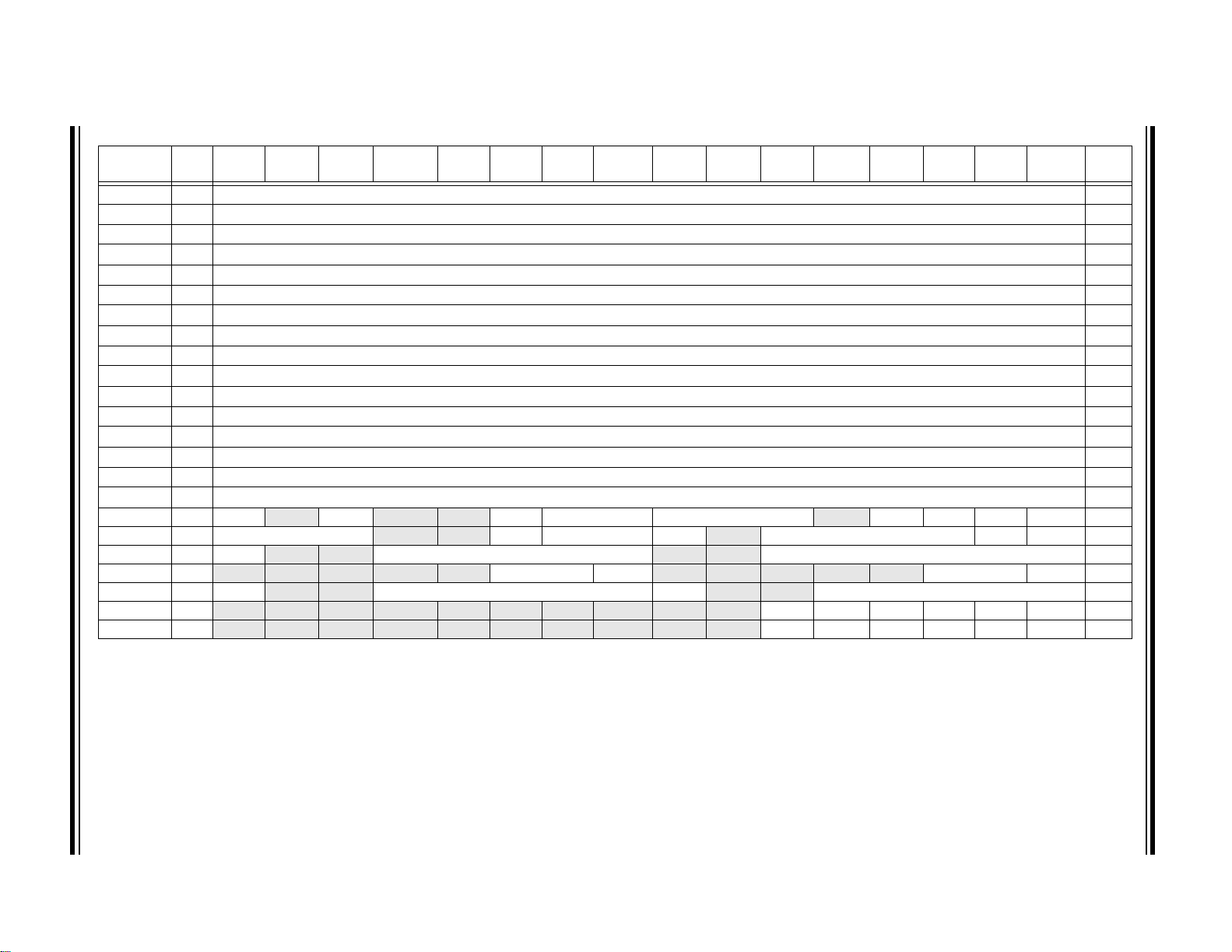
File Name Addr Bit 15 Bit 14 Bit 13 Bit 12 Bit 11 Bit 10 Bit 9 Bit 8 Bit 7 Bit 6 Bit 5 Bit 4 Bit 3 Bit 2 Bit 1 Bit 0
NVMCON 0760 WR WREN WRERR — — — — — — ERASE — —NVMOP<3:0>
NVMKEY 0766
Legend: x = unknown value on Reset, — = unimplemented, read as ‘0’. Reset values are shown in hexadecimal.
Note 1: Reset value shown is for POR only. Value on other Reset states is dependent on the state of memory write or erase operations at the time of Reset.
— — — — — — — — NVMKEY<7:0>
All
Resets
0000
0000
(1)
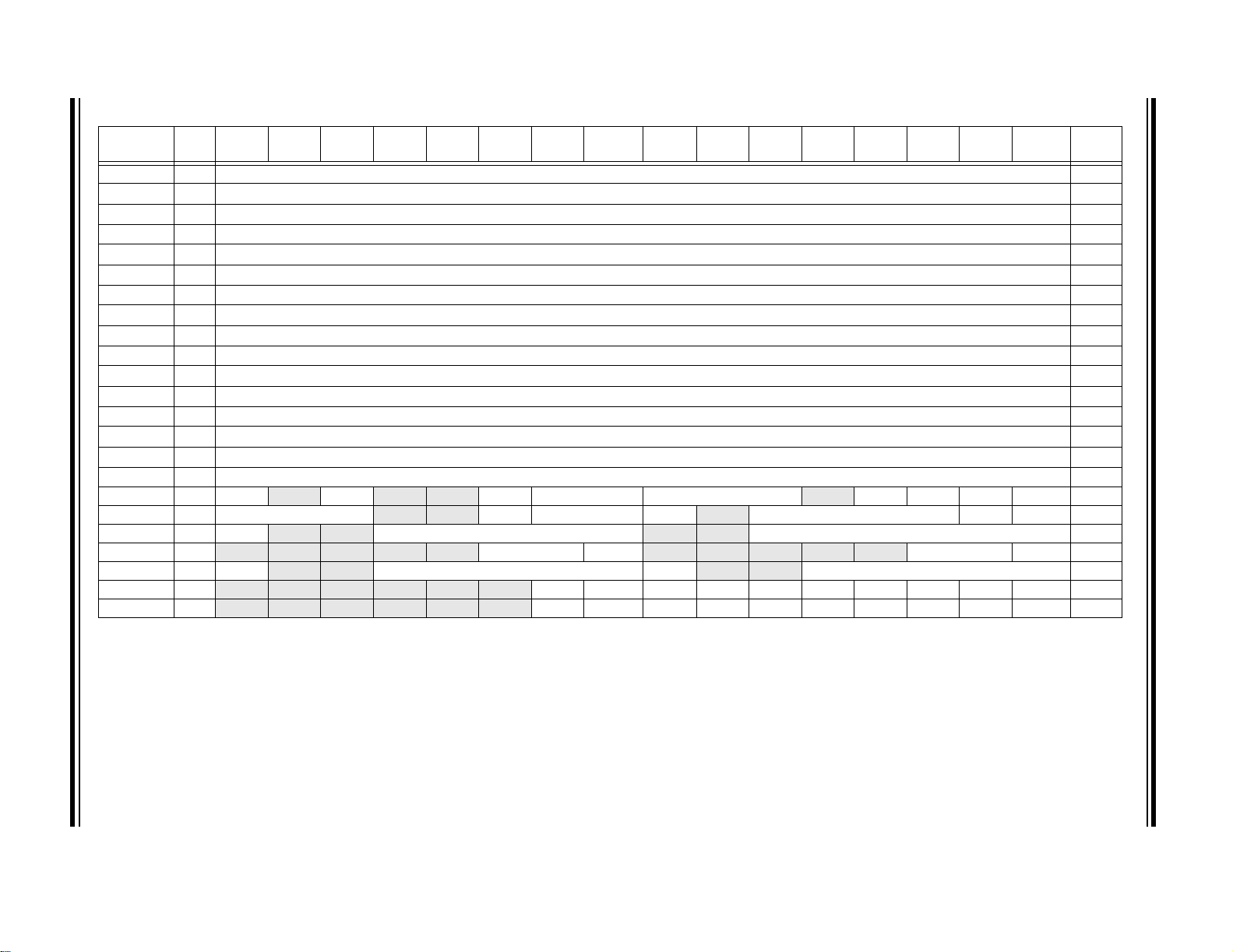
TABLE 3-21: PMD REGISTER MAP
File Name Addr Bit 15 Bit 14 Bit 13 Bit 12 Bit 11 Bit 10 Bit 9 Bit 8 Bit 7 Bit 6 Bit 5 Bit 4 Bit 3 Bit 2 Bit 1 Bit 0
PMD1 0770
PMD2 0772 IC8MD IC7MD
Legend: x = unknown value on Reset, — = unimplemented, read as ‘0’. Reset values are shown in hexadecimal.
— —
T3MD T2MD T1MD
— — — —IC2MDIC1MD— — — — — —OC2MDOC1MD0000
— — —
I2C1MD
—
U1MD
—
SPI1MD
— —
AD1MD 0000
All
Resets

PIC24HJ12GP201/202
3.2.5 SOFTWARE STACK
In addition to its use as a working register, the W15
register in the PIC24HJ12GP201/202 devices is also
used as a software Stack Pointer. The Stack Pointer
always points to the firs t avai lable free w ord and gro ws
from lower to higher addresses. It pre-decrements for
stack pops and post-increments for stack pushes, as
shown in Figure 3-4. For a PC push during any CALL
instruction, the M SB o f t he PC i s ze ro-extended before
the push, ensuring that the MSB is always clear.
Note: A PC push during exception processing
concatenates the SRL regis ter to th e MSB
of the PC prior to the push.
The Stack Pointer Limit register (SPLIM) associated
with the Stack Pointer sets an upper address boundary
for the stack. SPLIM is uninitialized at Reset. As is the
case for the Stack Pointer, SPLIM<0> is forced to ‘0’
because all stack operations must be word-aligned.
When an EA is generated using W15 as a source or
destination pointer, the resulting address is compared
with the value in SPLIM. If the contents of the Stack
Pointer (W15) and the SPLIM register are equal and a
push operation is performed, a stack error trap will not
occur. The stack error tra p will occ ur on a subs equen t
push operation. For example, to cause a stack error
trap when the stack grows beyond address 0x2000 in
RAM, initialize the SPLIM with the value 0x1FFE.
Similarly, a Stack Pointer underflow (sta ck error) tra p is
generated when the Stack Pointer address is found to
be less than 0x0800. This prevents the stack from
interfering with the Special Function Register (SFR)
space.
A write to the SPLIM regis ter should not be immediately
followed by an indirect read operation using W15.
FIGURE 3-4: CALL STACK FRAME
0x0000
Stack Grows Toward
000000000
Higher Address
PC<15:0>
PC<22:16>
<Free Word>
015
W15 (before CALL)
W15 (after CALL)
POP : [--W15]
PUSH : [W15++]
3.2.6 DATA RAM PROTECTION FEATURE
The PIC24H product family supports Data RAM
protection features that enable segme nts of RAM to be
protected when used in conjunction with Boot and
Secure Code Segm ent Secu rity. BSRAM (Secure RAM
segment for BS) is accessible only from the Boot
Segment Flas h code when en abled. SSRA M (Secure
RAM segment for RAM) is accessible only from the
Secure Segment Flash code when enabled. See
Table 3-1 for an overview of the BSRAM and SSRAM
SFRs.
3.3 Instruction Addressing Modes
The addressing modes shown in Table 3-22 form the
basis of the addressi ng modes optimized to support the
specific features of individual instructions. The
addressing modes prov ided in the MAC class of instructions differ from those in the other instruction types.
3.3.1 FILE REGISTER INSTRUCTIONS
Most file register ins truc tio ns use a 13-bit address field
(f) to directly address data present in the first 8192
bytes of data memory (Near Data Space). Most file
register instructions employ a working register, W0,
which is de noted as WREG i n these instruc tions. The
destination is typically either the same file register or
WREG (with the exception of the MUL instruction),
which writes the re sult t o a re gister or regi ster p air. The
MOV instruction allows additional flexibility and can
access the entire data space.
3.3.2 MCU INSTRUCTIONS
The three-operand MCU instructions are of the form:
Operand 3 = Operand 1 <function> Operand 2
where Operand 1 is always a working register (that is,
the addressing mode can only be register direct ), which
is referred to as Wb. Operand 2 can be a W register,
fetched from data memory, or a 5-bit literal. The result
location can be either a W register or a data memory
location. The following addressing modes are
supported by MCU instructions:
• Register Direct
• Register Indirect
• Register Indirect Post-Modified
• Register Indirect Pre-Modified
• 5-bit or 10-bit Literal
Note: Not all instructions support all the
addressing modes given above. Individual
instructions can support different subsets
of these addressing modes.
© 2007 Microchip Technology Inc. Advance Information DS70282A-page 31

PIC24HJ12GP201/202
TABLE 3-22: FUNDAMENTAL ADDRESSING MODES SUPPORTED
Addressing Mode Description
File Register Direct The address of the file register is specified explicitly.
Register Direct The contents of a register are accessed directly.
Register Indirect The contents of Wn forms the Effective Address (EA.)
Register Indirect Post-Modified The contents of Wn forms the EA. Wn is post-modified (incremented or
decremented) by a constant value.
Register Indirect Pre-Modified Wn is pre-modified (incremented or decremented) by a signed constant value
to form the EA.
Register Indirect with Register Offset
(Register Indexed)
Register Indirect with Literal Offset The sum of Wn and a literal forms the EA.
The sum of Wn and Wb forms the EA.
3.3.3 MO VE (MOV) INSTRUCTION
Move instruction s provide a greater degre e of addres sing flexibility than other instructions. In addi tion to the
addressing modes supported by most MCU instructions, MOV instructions also support Register Indirect
with Register Offset Addr ess in g mod e, also referred to
as Register Indexed mode.
Note: For the MOV instructions, the addressing
mode specified in the instruction can differ
for the source and destination EA.
However, the 4-bit Wb (Register Offset)
field is shared by both source and
destination (but typically only used by
one).
In summary, the following addressing modes are
supported by move instructions:
• Register Direct
• Register Indirect
• Register Indirect Post-modified
• Register Indirect Pre-modified
• Register Indirect with Register Offset (Indexed)
• Register Indirect with Literal Offset
• 8-bit Literal
• 16-bit Literal
Note: Not all instructions sup port all the addr ess-
ing modes given abo ve. Ind ividu al ins tructions may support different subsets of
these addressing modes.
3.3.4 OTHER INSTRUCTIONS
Besides the addressing modes outlined previously, some
instructions use literal constants of various sizes. For
example, BRA (branch) instructions use 16-bit signed literals to specify the branch destination directly, whereas
the DISI instruction uses a 14-bit unsigned literal field. In
some instructio ns, such as ADD Acc, the sourc e of an
operand or resu lt is imp li ed by the o pco de itse lf. Cer tain
operations, s uc h as NOP, do not have any operands.
DS70282A-page 32 Advance Information © 2007 Microchip Technology Inc.

PIC24HJ12GP201/202
3.4 Interfacing Program and Data Memory Spaces
The PIC24HJ12GP201/202 architecture uses a 24-bitwide program sp ace and a 16-bit -wide dat a sp ace. Th e
architecture is also a modified Harvard scheme, meaning that data c an also b e prese nt in the p rogram sp ace.
To use this data successfully, it must be accessed in a
way that preserv es th e ali gnmen t of i nforma tio n in both
spaces.
Aside from normal execution, the PIC24HJ12GP201/
202 architecture provides two methods by which program space can be accessed during operation:
• Using table in stru ctions to ac cess in divid ual bytes
or words anywhere in the program space
• Remapping a portion of the program spac e into
the data space (Program Space Visibility)
Table instructions allow an application to read or write
to small areas of the program memory. This capability
makes the method ideal for accessing data tables that
need to be upd ated perio dically. It also all ows access
to all bytes of the program word. The remapping
method allows an applicat ion to ac cess a l arge bloc k of
data on a read-only basis, which is ideal for look ups
from a large table of static data. The application can
only access the least significant word of the program
word.
3.4.1 ADDRESSING PROGRAM SPACE
Since the address ranges for the data and program
spaces are 16 and 24 bits, respectively, a method is
needed to create a 23-bit or 24-bit program address
from 16-bit data regist ers. The solution de pends on the
interface method to be used.
For table operations, the 8-bit Table Page register
(TBLPAG) is used to define a 32K word region within
the program space. This is concatenated with a 16-bit
EA to arrive at a full 24-bit program space address. In
this format, the Most Significant bit of TBLPAG is used
to determine if the ope ration occurs in the user memory
(TBLPAG<7> = 0) or the configuration memory
(TBLPAG<7> = 1).
For remapping operations, the 8-bit Program Space
Visibility register (PSVPAG) is used to define a
16K word page in the program space. When the Most
Significant bit of th e EA is ‘1’, PSVPAG is concaten ated
with the lower 15 b its of t he EA to form a 23-bit program
space address. Unlike table operations, this limits
remapping operati ons stric tly to the u ser m emory area.
T abl e 3-23 and Fig ure 3-5 show how the program EA is
created for table operations and remapping accesses
from the data EA. Here, P<23:0> refers to a program
space word, and D<15:0> refers to a data space word.
TABLE 3-23: PROGRAM SPACE ADDRESS CONSTRUCTION
Access Type
Instruction Access
(Code Execution)
TBLRD/TBLWT
(Byte/Word Read/Write)
Program Space Visibility
(Block Remap/Read)
Note 1: Data EA<15> is always ‘1’ in this case, but is not used in calcul ating th e progra m sp ace a ddress . Bit 15 of
the address is PSVPAG<0>.
Access
Space
User 0 PC<22:1> 0
User TBLPAG<7:0> Data EA<15:0>
Configuration TBLPAG<7:0> Data EA<15:0>
User 0 PSVPAG<7:0> Data EA<14:0>
<23> <22:16> <15> <14:1> <0>
0xx xxxx xxxx xxxx xxxx xxx0
0xxx xxxx xxxx xxxx xxxx xxxx
1xxx xxxx xxxx xxxx xxxx xxxx
0 xxxx xxxx xxx xxxx xxxx xxxx
Program Space Address
(1)
© 2007 Microchip Technology Inc. Advance Information DS70282A-page 33

PIC24HJ12GP201/202
FIGURE 3-5: DATA ACCESS FROM PROGRAM SPACE ADDRESS GENERATION
Program Counter
Table Operations
Program Space Visibility
(Remapping)
(1)
(2)
User/Configuration
0
1/0
(1)
0
Space Select
TBLPAG
8 bits
Select
PSVPAG
8 bits
23 bits
24 bits
1
23 bits
EA
16 bits
EA
15 bits
0Program Counter
1/0
0
Byte Select
Note 1: The Least Significant bit (LSb) of program space addresses is always fixed as ‘0’ to
maintain word alignment of data in the program and data spaces.
2: Table operations are not required t o b e w o rd-al ign ed . Table read ope rati on s a r e p ermitted
in the configuration memory space.
DS70282A-page 34 Advance Information © 2007 Microchip Technology Inc.

PIC24HJ12GP201/202
3.4.2 DATA ACCESS FROM PROGRAM
MEMORY USING TABLE
INSTRUCTIONS
The TBLRDL and TBLWTL instructions offer a direct
method of reading or writing the lower word of any
address within the program space without going
through data space. The TBLRDH and TBLWTH
instructions are the only method to read or write the
upper 8 bits of a program space word as data.
The PC is incremented by two for each successive
24-bit program word. This allows program memory
addresses to directly map to data space addresses.
Program memor y can th us be rega rded as two 16- bitwide word address sp ac es , res id ing sid e by si de, eac h
with the same address range. TBLRDL and TBLWTL
access the space that contains the least significant
data word. TBLRDH and TBLWTH access the space that
contains the upper data byte.
Two table instructions are provided to move byte or
word-sized (16-bit) data to and from program space.
Both function as either byte or word operations.
• TBLRDL (Table Read Low): In Word mode, this
instruction maps the lower word of the program
space location (P<15:0> ) to a data addre ss
(D<15:0>).
In Byte mode, either the upper or lo wer byte of th e
lower program word is mapped to th e lower byte of
a data address. The upper byte is selected when
Byte Select is ‘1’; the lower byte is selected when
it is ‘0’.
• TBLRDH (Table Read High): In Word m o d e , th i s
instruction maps the entire upper word of a program
address (P<23:16>) to a data address. Note that
D<15:8>, the ‘phantom byte’, will always be ‘0’.
In Byte mode, this instruction maps the upper or
lower byte of the program word to D<7:0> of the
data address, as in the TBLRDL instruction. Note
that the data will always be ‘0’ when the upper
‘phantom’ byte is selected (Byte Select = 1).
In a similar fashion, two table instructions, TBLWTH
and TBLWTL, are used to write individual bytes or
words to a program space address. The details of
their operati on are explained in Section 4.0 “Flash
Program Memory”.
For all table operations, the area of program memory
space to be access ed is de termine d by the Table Page
register (TBLPAG). TBLPAG cov ers the entire pro gram
memory space of t he device, in cluding use r and confi guration spaces. W hen TBL PAG<7> = 0, the table page
is located in the user memory space. When
TBLPAG<7> = 1, the page is located in configuration
space.
FIGURE 3-6: ACCESSING PROGRAM MEMORY WITH TABLE INSTRUCTIONS
TBLPAG
02
23 15 0
0x000000
0x020000
0x030000
0x800000
Program Space
00000000
00000000
00000000
00000000
‘Phantom’ By te
TBLRDH.B (Wn<0> = 0)
TBLRDL.B (Wn<0> = 1)
TBLRDL.B (Wn<0> = 0)
TBLRDL.W
The address for the table operation is determined by the data EA
within the page defined by the TBLPAG register.
Only read operations are shown; write operations are also valid in
the user memory area.
081623
© 2007 Microchip Technology Inc. Advance Information DS70282A-page 35

PIC24HJ12GP201/202
3.4.3 READING DATA FROM PROGRAM
MEMORY USING PROGRAM SPACE
VISIBILITY
The upper 32 Kbytes of data space may optionally be
mapped into any 1 6K word page of the program spac e.
This option provides tran sparent access to stored constant data from the data space without the need to use
special instructions (such as TBLRDL/H).
Program space access through the data space occurs
if the Most Significan t bit of the dat a space EA i s ‘1’ and
program spac e visibil ity is enabl ed by se tting t he PSV
bit in the Core Control register (CORCON<2>). The
location of th e program memory spac e to be mapped
into the data space is determined by the Program
Space Visibility Page register (PSVPAG). This 8-bit
register defines any one of 256 possible pages of
16K words in program space. In effect, PSVPAG
functions as the upper 8 bits of the program memory
address, with the 15 bits of the EA functioning as the
lower bits. By incrementing the PC by 2 for each
program memory word, the low e r 15 bits of data space
addresses directly map to the lower 15 bits in the
corresponding program space addresses.
Data reads to this area add a cycle to the instruction
being executed, since two program memory fetches
are required.
Although each data space address 8000h and higher
maps directly into a corresponding program memory
address (see Figure 3-7), only the lower 16 bits of the
24-bit program word are used to contain the data. The
upper 8 bits of any program space location used as
data should be programmed with ‘1111 1111’ or
‘0000 0000’ to force a NOP. This prevents possible
issues should the area of code ever be accidentally
executed.
Note: PSV access is temporarily disabled durin g
table reads/writes.
For operations that use PSV and are executed outside
a REPEAT loop, the MOV and MOV.D instructions
require one instructio n cycle in additi on to the sp ecified
execution time. All other instructions require two
instruction cycles in addition to the specified execution
time.
For operations that use PSV, and are executed inside
a REPEAT loop, the se in stances require two instruction
cycles in addition to the spe ci fie d ex ec uti on time of the
instruction:
• Execution in the first iteration
• Execution in the last iteration
• Execution prior to exiting the loop due to an
interrupt
• Execution upon re-entering the loop after an
interrupt is serviced
Any other iteration of the REPEAT loop will allow the
instruction using PSV to access data to execute in a
single cycle.
FIGURE 3-7: PROGRAM SPACE VISIBILITY OPERATION
When CORCON<2> = 1 and EA<15> = 1:
Program Space
PSVPAG
02
The data in the page
designated by
PSVPAG is mapped
into the upper half of
the data memory
space...
23 15 0
0x000000
0x010000
0x018000
0x800000
Data Space
PSV Area
0x0000
0x8000
0xFFFF
Data EA<14:0>
...while the lower 15 bits
of the EA specify an
exact address within
the PSV area. This
corresponds exactly to
the same lower 15 bits
of the actual program
space address.
DS70282A-page 36 Advance Information © 2007 Microchip Technology Inc.

PIC24HJ12GP201/202
4.0 FLASH PROGRAM MEMORY
Note: This data sheet summarizes the features
of the PIC24HJ12GP201/2 02 devices. It i s
not intended to be a co mp rehe ns iv e re ference source. To complement the information in this dat a sheet, refe r to the “PIC24H
Family Reference Manual”. Please see
the Microchip web site (www.microchip.com) for the latest PIC24H Family
Reference Manual chap ters.
The PIC24HJ12GP201/202 devices contain internal
Flash program memory for storing an d executi ng application code. The memory is readable, writable and
erasable during normal operation over the entire V
range.
Flash memory can be programmed in two ways:
• In-Circuit Serial Programming™ (ICSP™)
programming capability
• Run-Time Self-Programming (RTSP)
ICSP allows a PIC24HJ12GP201/202 device to be
serially programme d while in the en d application circuit.
This is done with two lines for programming clock and
programming data (one of the alt ernate pro gramming
pin pairs: PGC1/PGD1, PGC2/ PGD2 or PGC3/PGD3),
and three other lines fo r power (V
Master Clear (MCLR
). This allows customers to manu-
DD), ground (VSS) and
facture boards with unprogrammed devices and then
program the digit al signal con troller just befo re shipping
the product. This also allows the most recent firmware
or a custom firmware to be programmed.
DD
RTSP is accomplished using TBLRD (table read) and
TBLWT (table write) instructions. With RTSP, the user
application can write program memory data either in
blocks or ‘rows’ of 64 instructions (192 bytes) at a time
or a single program memory word, and erase program
memory in blocks or ‘pages’ of 512 instructions (1536
bytes) at a time.
4.1 Table Instructions and Flash
Programming
Regardless of the method used, all programming of
Flash memory is done with the table read and table
write instructions. These allow direct read and write
access to the program memory space from the data
memory while the device is in normal operating mode.
The 24-bit target address in the program memory is
formed using bit s <7:0> of the TBLP AG re gister and the
Effective Address (EA) from a W register specified in
the table instruction, as shown in Figure 4-1.
The TBLRDL and the TBLWTL instructions are used to
read or write to bits<15:0> of program memory.
TBLRDL and TBLWTL can access program memory in
both Word and Byte modes.
The TBLRDH and TBLWTH i nstructio ns are used to read
or write to bits<23:16> of program memory. TBLRDH
and TBLWTH can also access prog ram memory in Word
or Byte mode.
FIGURE 4-1: ADDRESSING FOR TABLE REGISTERS
24 bits
Using
Program Counter
Using
Table Instruction
User/Configuration
Space Select
0
1/0
TBLPAG Reg
8 bits
Program Counter
Working Reg EA
24-bit EA
0
16 bits
Byte
Select
© 2007 Microchip Technology Inc. Advance Information DS70282A-page 37

PIC24HJ12GP201/202
4.2 RTSP Operation
The PIC24HJ12GP201/202 Flash program memory
array is organized into rows of 64 instructions or 192
bytes. RTSP allows the user application to erase a
page of memory, which consists of eight rows (512
instructions) at a time, and to program one row or one
word at a time. The 8-row erase pages and single row
write rows are edge-aligned from the beginning of program memory, on boundaries of 1536 bytes and 192
bytes, respectively.
The program memory implements holding buffers that
can contain 64 instructions of programming data. Prior
to the actual programming operation, the write data
must be loaded into the buffers sequentially. The
instruction words loaded must always be from a group
of 64 boundary.
The basic sequence f or RTSP program ming is to set up
a Table Pointer, then do a series of TBLWT instructions
to load th e buffer s. P rogram ming i s per for med by setting the control bits in the NVMCON register. A total of
64 TBLWTL and TBLWTH i nstruc tions are requ ired t o
load the instructions.
All of the table write operations are single-word writes
(two instruction cycles) because only the buffers are
written. A programming cycle is required for
programming each row.
4.3 Control Registers
Two SFRs are used to read and write the program
Flash memory:
• NVMCON: Flash Memory Control Register
• NVMKEY: NonVolatile Memory Key Register
The NVMCON register (Register 4-1) controls which
blocks are to be erased, which memory type is to be
programmed and the start of the programming cycle.
NVMKEY (Register 4-2) is a write-only register that is
used for write protection. To start a programming or
erase sequence, the user application must consecutively write 55h and AAh to the NVMKEY register . Refer
to Section 4.4 “Programming Operations” for further
details.
4.4 Programming Operations
A complete programming sequence is necessary for
programming or erasing the internal Flash in RTSP
mode. A programming operation is nominally 4 ms in
duration and the processor stalls (waits) until the operation is finished. Setting the WR bit (NVMCON<15>)
starts the operation, and the WR bit is automatically
cleared when the operation is finished.
DS70282A-page 38 Advance Information © 2007 Microchip Technology Inc.

PIC24HJ12GP201/202
REGISTER 4-1: NVM CON: FLASH MEMORY CONTROL REGISTER
R/SO-0
(1)
WR WREN WRERR — — — — —
bit 15 bit 8
R/W-0
(1)
R/W-0
(1)
U-0 U-0 U-0 U-0 U-0
U-0 R/W-0
(1)
U-0 U-0 R/W-0
— ERASE — —NVMOP<3:0>
(1)
R/W-0
(1)
R/W-0
(2)
(1)
R/W-0
(1)
bit 7 bit 0
Legend: SO = Satiable only bit
R = Readable bit W = Writable bit U = Unimplemented bit, read as ‘0’
-n = Value at POR ‘1’ = Bit is set ‘0’ = Bit is cleared x = Bit is unknown
bit 15 WR: Write Control bit
1 = Initiates a Flash memory program or erase operation. The operation is self-timed and the bit is
cleared by hardware once operation is complete.
0 = Program or erase operation is complete and inactive
bit 14 WREN: Write Enable bit
1 = Enable Flash program/erase operations
0 = Inhibit Flash program/erase operations
bit 13 WRERR: Write Sequence Error Flag bit
1 = An improper program or erase sequence attempt or termination has occurred (bit is set
automatically on any set attempt of the WR bit)
0 = The program or erase operation completed normally
bit 12-7 Unimplemented: Read as ‘0’
bit 6 ERASE: Erase/Program Enable bit
1 = Perform the erase operation specified by NVMOP<3:0> on the next WR command
0 = Perform the program operation specified by NVMOP<3:0> on the next WR command
bit 5-4 Unimplemented: Read as ‘0’
(2)
bit 3-0 NVMOP<3:0>: NVM Operation Select bits
If ERASE =
1:
1111 = Memory bulk erase operation
1101 = Erase General Segment
1100 = Erase Secure Segment
0011 = No operation
0010 = Memory page erase operation
0001 = No operation
0000 = Erase a single Configuration register byte
If ERASE =
0:
1111 = No operation
1101 = No operation
1100 = No operation
0011 = Memory word program operation
0010 = No operation
0001 = Memory row program operation
0000 = Program a single Configuration register byte
Note 1: These bits can only be Reset on POR.
2: All other combinations of NVMOP<3:0> are unimplemented.
© 2007 Microchip Technology Inc. Advance Information DS70282A-page 39

PIC24HJ12GP201/202
REGISTER 4-2: NVMKEY: NONVOLATILE MEMORY KEY REGISTER
U-0 U-0 U-0 U-0 U-0 U-0 U-0 U-0
— — — — — — — —
bit 15 bit 8
W-0 W-0 W-0 W-0 W-0 W-0 W-0 W-0
NVMKEY<7:0>
bit 7 bit 0
Legend: SO = Satiable only bit
R = Readable bit W = Writable bit U = Unimplemented bit, read as ‘0’
-n = Value at POR ‘1’ = Bit is set ‘0’ = Bit is cleared x = Bit is unknown
bit 15-8 Unimplemented: Read as ‘0’
bit 7-0 NVMKEY<7:0>: Key Register (write-only) bits
DS70282A-page 40 Advance Information © 2007 Microchip Technology Inc.

PIC24HJ12GP201/202
4.4.1 PROGRAMMING ALGORITHM FOR
FLASH PROGRAM MEMORY
Programmers can program one row of program Flash
memory at a time. To do this, it is necessary to erase
the 8-row erase page that contains the desired row.
The general process is:
1. Read eight rows of program memory
(512 instructions) and store in data RAM.
2. Update the program data in RAM with the
desired new data.
3. Erase the block (see Example 4-1):
a) Set the NVMOP bits (NVMCON<3:0>) to
‘0010’ to configure for block erase. Set the
ERASE (NVMCON<6>) and WREN
(NVMCON<14>) bits.
b) Write the starting add res s o f th e page to be
erased into the TBLPAG and W registers.
c) Write ‘55h’ to NVMKEY.
d) Write ‘AAh’ to NVMKEY.
e) Set the WR bit (NVMCON<15>). The erase
cycle begins and the CPU s t al l s fo r t he d u r a-
tion of the erase cycle. When the erase is
done, the WR bit is cleared automatically.
4. Write the first 64 instruc tions from dat a RAM in to
the program memory b uffers (see Example 4-2).
5. Write the program block to Flash memory:
a) Set the NVMOP bits to ‘0001’ to configure
for row programming. Clear the ERASE bit
and set the WREN bit.
b) Write ‘55h’ to NVMKEY.
c) Write ‘AAh’ to NVMKEY.
d) Set the WR bit. The programming cycle
begins and th e CPU stalls for the duration of
the write cycl e. When the wr ite to Flash mem -
ory is done, the WR bit is cleared
automatically.
6. Repeat steps 4 and 5, using the next available
64 instructi ons from the block in data R AM by
incrementing the value in TBLPAG, until all
512 instructions are written back to Flash memory.
For protection against accidental operations, the write
initiate sequence for NVMKEY must be used to allow
any erase or program operation to proceed. After the
programming command has been executed, the user
application must wait for the programming time until
programming is complete. The two instructions
following the start of the programming sequence
should be NOPs, as shown in Example 4-3.
EXAMPLE 4-1: ERASING A PROGRAM MEMORY PAGE
; Set up NVMCON for block erase operation
MOV #0x4042, W0 ;
MOV W0, NVMCON ; Initialize NVMCON
; Init pointer to row to be ERASED
MOV #tblpage(PROG_ADDR), W0 ;
MOV W0, TBLPAG ; Initialize PM Page Boundary SFR
MOV #tbloffset(PROG_ADDR), W0 ; Initialize in-page EA[15:0] pointer
TBLWTL W0, [W0] ; Set base address of erase block
DISI #5 ; Block all interrupts with priority <7
; for next 5 instructions
MOV #0x55, W0
MOV W0, NVMKEY ; Write the 55 key
MOV #0xAA, W1 ;
MOV W1, NVMKEY ; Write the AA key
BSET NVMCON, #WR ; Start the erase sequence
NOP ; Insert two NOPs after the erase
NOP ; command is asserted
© 2007 Microchip Technology Inc. Advance Information DS70282A-page 41

PIC24HJ12GP201/202
EXAMPLE 4-2: LOADING THE WRITE BUFFERS
; Set up NVMCON for row programming operations
; Set up a pointer to the first program memory location to be written
; program memory selected, and writes enabled
; Perform the TBLWT instructions to write the latches
; 0th_program_word
; 1st_program_word
; 2nd_program_word
; 63rd_program_word
MOV #0x4001, W0 ;
MOV W0, NVMCON ; Initialize NVMCON
MOV #0x0000, W0 ;
MOV W0, TBLPAG ; Initialize PM Page Boundary SFR
MOV #0x6000, W0 ; An example program memory address
MOV #LOW_WORD_0, W2 ;
MOV #HIGH_BYTE_0, W3 ;
TBLWTL W2, [W0] ; Write PM low word into program latch
TBLWTH W3, [W0++] ; Write PM high byte into program latch
MOV #LOW_WORD_1, W2 ;
MOV #HIGH_BYTE_1, W3 ;
TBLWTL W2, [W0] ; Write PM low word into program latch
TBLWTH W3, [W0++] ; Write PM high byte into program latch
MOV #LOW_WORD_2, W2 ;
MOV #HIGH_BYTE_2, W3 ;
TBLWTL W2,
TBLWTH W3,
•
•
•
MOV #LOW_WORD_31, W2 ;
MOV #HIGH_BYTE_31, W3 ;
TBLWTL W2,
TBLWTH W3,
[W0] ; Write PM low word into program latch
[W0++] ; Write PM high byte into program latch
[W0] ; Write PM low word into program latch
[W0++] ; Write PM high byte into program latch
EXAMPLE 4-3: INITIATING A PROGRAMMING SEQUENCE
DISI #5 ; Block all interrupts with priority <7
MOV #0x55, W0
MOV W0, NVMKEY ; Write the 55 key
MOV #0xAA, W1 ;
MOV W1, NVMKEY ; Write the AA key
BSET NVMCON, #WR ; Start the erase sequence
NOP ; Insert two NOPs after the
NOP ; erase command is asserted
; for next 5 instructions
DS70282A-page 42 Advance Information © 2007 Microchip Technology Inc.

PIC24HJ12GP201/202
5.0 RESETS
Note: This data sheet summarizes the features
of the PIC24HJ12GP201/2 02 devices. It i s
not intended to be a co mp rehe ns iv e re ference source. To complement the information in this dat a sheet, refe r to the “PIC24H
Family Reference Manual”. Please see
the Microchip web site (www.microchip.com) for the latest PIC24H Family
Reference Manual chap ters.
The Reset module combines all Reset sources and
controls the device Master Reset Signa l, SYSRST
following is a list of device Reset sources:
• POR: Power-on Reset
• BOR: Brown-out Reset
•MCLR
: Master Clear Pin Reset
•SWR: RESET Instructi on
• WDTO: Watchdog Timer Reset
• TRAPR: Trap Conflict Reset
• IOPUWR: Illegal Opcode, Uninitialized W
Register Reset, and Security Reset
• CM: Configuration Mismatch Reset
A simplified block diagram of the Reset module is
shown in Figure 5-1.
. The
Any active source of Reset makes the SYSRST
signal
active. Many registers associated with the CPU and
peripherals are forced to a known Reset state. Most
registers are unaffected by a Reset; their status is
unknown on POR and unchanged by all other Resets.
Note: Refer to the specific peripheral or CPU
section of this manual for register Reset
states.
All types of device Res et will set a corresp onding statu s
bit in the RCON register to indicate the type of Reset
(see Register 5-1). A POR will clear all bits, except for
the POR bit (RCON<0>), that are set. The user application can set or clear any bit at any time during code
execution. The RCON bits only serve as status bits.
Setting a par ticular Reset statu s bit in software does
not cause a device Reset to occur.
The RCON register also has other bits associated with
the Watchdog Timer and device power-saving states.
The function of these bit s is discusse d in other section s
of this manual.
Note: The status bits in the RCON register
should be cleared after they are read so
that the next RCON register value after a
device Reset will be meaningful.
FIGURE 5-1: RESET SYSTEM BLOCK DIAGRAM
RESET Instruction
Glitch Filter
MCLR
WDT
Module
Sleep or Idle
VDD Rise
VDD
Uninitialized W Register
Configuration Mismatch
Detect
Internal
Regulator
Trap Conflict
Illegal Opcode
POR
BOR
SYSRST
© 2007 Microchip Technology Inc. Advance Information DS70282A-page 43

PIC24HJ12GP201/202
REGISTER 5-1: RCON: RESET CONTROL REGISTER
R/W-0 R/W-0 U-0 U-0 U-0 U-0 R/W-0 R/W-0
TRAPR IOPUWR — — — —CMVREGS
bit 15 bit 8
R/W-0 R/W-0 R/W-0 R/W-0 R/W-0 R/W-0 R/W-1 R/W-1
(2)
EXTR SWR SWDTEN
bit 7 bit 0
Legend:
R = Readable bit W = Writable bit U = Unimplemented bit, read as ‘0’
-n = Value at POR ‘1’ = Bit is set ‘0’ = Bit is cleared x = Bit is unknown
bit 15 TRAPR: Trap Reset Flag bit
1 = A Trap Conflict Reset has occurred
0 = A Trap Conflict Reset has not occurred
bit 14 IOPUWR: Illegal Opcode or Un initialized W Access Reset Flag bit
1 = An illegal opcode detection, an illegal address mode or uninitialized W register used as an
Address Pointer caused a Reset
0 = An illegal opcode or uninitialized W Reset has not occurred
bit 13-10 Unimplemented: Read as ‘0’
bit 9 CM: Configuration Mismatch Flag bit
1 = A configuration mismatch Reset has occurred.
0 = A configuration mismatch Reset has NOT occurred.
bit 8 VREGS: Voltage Regulator Standby D uring Sleep bit
1 = Voltage regulator is active during Sleep
0 = Voltage regulator goes into Standby mode during Sleep
bit 7 EXTR: External Reset (MCLR
1 = A Master Clear (pin) Reset has occurred
0 = A Master Clear (pin) Reset has not occurred
bit 6 SWR: Software Reset (Instruction) Flag bit
1 = A RESET instruction has been executed
0 = A RESET instruction has not been executed
bit 5 SWDTEN: Software Enable/Disable of WDT bit
1 = WDT is enabled
0 = WDT is disabled
bit 4 WDTO: Watchdog Timer Time-out Flag bit
1 = WDT time-out has occurred
0 = WDT time-out has not occurred
bit 3 SLEEP: Wake-up from Sleep Flag bit
1 = Device has been in Sleep mode
0 = Device has not been in Sleep mode
bit 2 IDLE: Wake-up from Idle Flag bit
1 = Device was in Idle mode
0 = Device was not in Idle mode
Note 1: All of the Reset status bits c an be set or cl eared in softw are. Setti ng one of the se bits in softw are does not
cause a device Reset.
2: If the FWDTEN Configuration bit is ‘1’ (unprogrammed), the WDT is always enabled, regardl ess of the
SWDTEN bit setting.
WDTO SLEEP IDLE BOR POR
) Pin bit
(1)
(2)
DS70282A-page 44 Advance Information © 2007 Microchip Technology Inc.

PIC24HJ12GP201/202
REGISTER 5-1: RCON: RESET CONTROL REGISTER
bit 1 BOR: Brown-out Reset Flag bit
1 = A Brown-out Reset has occurred
0 = A Brown-out Reset has not occurred
bit 0 POR: Power-on Reset Flag bit
1 = A Power-up Reset has occurred
0 = A Power-up Reset has not occurred
Note 1: All of the Reset status bits c an be set or cl eared in softw are. Setti ng one of the se bits in softw are does not
cause a device Reset.
2: If the FWDTEN Configuration bit is ‘1’ (unprogrammed), the WDT is always enabled, regardless of the
SWDTEN bit setting.
TABLE 5-1: RESET FLAG BIT OPERATION
Flag Bit Setting Event Clearing Event
TRAPR (RCON<15>) Trap conflict event POR, BOR
IOPUWR (RCON<14>) Illegal opcode or uninitialized
W register access
CM (RCON<9>) Conf igu ration mismatch POR, BOR
EXTR (RCON<7>) MCLR Rese t POR
SWR (RCON<6>) RESET instruction POR, BOR
WDTO (RCON<4>) WDT time-out PWRSAV instruction, POR, BOR,
SLEEP (RCON<3>) PWRSAV #SLEEP instruction POR, BOR
IDLE (RCON<2>) PWRSAV #IDLE instruction POR, BOR
BOR (RCON<1>) BOR —
POR (RCON<0>) POR —
Note 1: All Reset flag bits may be set or cleared by the user software.
(1)
(1)
POR, BOR
CLRWDT instruction
© 2007 Microchip Technology Inc. Advance Information DS70282A-page 45

PIC24HJ12GP201/202
5.1 Clock Source Selection at Reset
If clock switching is enabled, the system clock source at
device Reset is chosen as shown in Table 5-2. If clock
switching is disabled, the s ystem c lock sou rc e i s always
selected according to the oscillator Configuration bits.
Refer to Section 7.0 “Oscillator Configuration” for
further details.
5.2 Device Reset Times
The Reset times for various types of device Reset are
summarized in Table 5-3. The system Reset signal,
SYSRST
times expi re.
The time at which the de vice actuall y begins to execu te
code also depends on the system oscillator delays,
, is released after the POR and PWRT delay
which include the Oscillator Start-up Timer (OST) and
TABLE 5-2: OSCILLATOR SELECTION vs.
TYPE OF RESET (CLOCK
SWITCHING ENABLED)
Reset Type Clock Source Determinant
POR Oscillator Configuration bits
BOR
MCLR
WDTR
(FNOSC<2:0>)
COSC Control bits
(OSCCON<14:12>)
the PLL lock time. The OST and PLL lock times occur
in parallel with the applicable SYSRST
The FSCM delay determines the time at which the
FSCM begins to monitor the system clock source after
the SYSRST
signal is released.
SWR
TABLE 5-3: RESET DELAY TIMES FOR VARIOUS DEVICE RESETS
Reset Type Clock Source SYSRST Delay
POR
POR EC, FRC, LPRC T
ECPLL, FRCPLL T
+ TSTARTUP + TRST ——1, 2, 3
POR
+ TSTARTUP + TRST TLOCK TFSCM 1, 2, 3, 5, 6
System Clock
Delay
XT, HS, SOSC TPOR + TSTARTUP + TRST TOST TFSCM 1, 2, 3, 4, 6
XTPLL, HSPLL TPOR + TSTARTUP + TRST TOST + TLOCK TFSCM 1, 2, 3, 4, 5, 6
BOR EC, FRC, LPRC T
ECPLL, FRCPLL T
STARTUP + TRST ——3
STARTUP + TRST TLOCK TFSCM 3, 5, 6
XT, HS, SOSC TSTARTUP + TRST TOST TFSCM 3, 4, 6
XTPLL, HSPLL TST ARTUP + TRST TOST + TLOCK TFSCM 3, 4, 5, 6
MCLR
WDT Any Clock T
Any Clock TRST ——3
RST ——3
Software Any Clock TRST ——3
Illegal Opcode Any Clock TRST ——3
Uninitialized W Any Clock T
RST ——3
Trap Conflict Any Clock TRST ——3
Note 1: TPOR = Power-on Reset delay (10 μs nom in al).
2: TSTARTUP = Conditional POR delay of 20 μs nominal (if on-chip regulator is enabled) or 64 ms nominal
Power-up Timer delay (if regu lator is disa bled). T
STARTUP is also applie d to a ll returns from powered-down
states, including waking from Sleep mode, only if the regulator is enabled.
3: T
RST = Internal state Reset time (20 μs nominal).
4: TOST = Oscillator Start-up Timer. A 10-bit counter counts 1024 oscillator periods before releasing the
oscillator clock to the system.
LOCK = PLL lock time (20 μs nominal).
5: T
6: TFSCM = Fail-Safe Clock Monitor delay (100 μs nominal).
FSCM
Delay
delay times.
Notes
DS70282A-page 46 Advance Information © 2007 Microchip Technology Inc.

PIC24HJ12GP201/202
5.2.1 POR AND LONG OSCILLATOR
START-UP TIMES
The oscillator st art-up circui try and its associat ed delay
timers are not linked to the device Reset delays that
occur at power-up. Some crystal circuits (especially
low-frequency crystals) have a relatively long start-up
time. Therefore, one or more of the following con ditions
is possible after SYSRST
• The oscillator circuit has not begun to oscillate.
• The Oscillator Start-up Timer has not expired (if a
crystal oscillator is used).
• The PLL has not achieved a lock (if PLL is used).
The device will not begin to execute code until a valid
clock source has been released to the system. Therefore, the oscillator and PLL start-up delays must be
considered when th e Reset del ay time mu st be known.
is released:
5.2.2 FAIL-SAFE CLOCK MONITOR
(FSCM) AND DEVICE RESETS
If the FSCM is enable d, it be gins t o moni tor the s ystem
clock source when SYSRST
source is not available at this time, the device automatically switches to the FRC oscillator and the user
application ca n switch to the desired crysta l oscillat or in
the Trap Service R outine.
is released. If a valid cloc k
5.2.2.1 FSCM Delay for Crystal and PLL
Clock Sources
When the system clock source is provided by a crystal
oscillator and/or t he PLL, a short d elay, T
matically inserted after the POR and PWRT delay
times. The FSCM does not be gin to monitor the system
clock source un til th is del ay expi res. Th e FSCM d elay
time is nominally 500 μs and provides additional time
for the oscillator and/ or PLL to st abil ize. In mos t cases ,
the FSCM delay prevents an oscillator failure trap at a
device Reset when the PWRT is disab led .
FSCM, is auto-
5.3 Special Function Register Reset
States
Most of the Special Function Registers (SFRs) associated with the CPU and peripherals are reset to a
particular value at a device Reset. The SFRs are
grouped by their peripheral or CPU function, and their
Reset values are specified in each section of this manual.
The Reset value for each SFR does not depend on the
type of Reset, with the exception of two registers:
• The Reset value for the Reset Control register,
RCON, depends on the type of device Reset.
• The Reset value for the Oscill ator Control re gister ,
OSCCON, depends on the type of Reset and the
programmed values of the Oscillator
Configuration bits in the FOSC Configuration
register.
© 2007 Microchip Technology Inc. Advance Information DS70282A-page 47

PIC24HJ12GP201/202
NOTES:
DS70282A-page 48 Advance Information © 2007 Microchip Technology Inc.

PIC24HJ12GP201/202
6.0 INTERRUPT CONTROLLER
Note: This data sheet summarizes the features
of the PIC24HJ12GP201/2 02 devices. It i s
not intended to be a co mp rehe ns iv e re ference source. To complement the information in this dat a sheet, refe r to the “PIC24H
Family Reference Manual”. Please see
the Microchip web site (www.microchip.com) for the latest PIC24H Family
Reference Manual chap ters.
The PIC24HJ12GP201/202 interrupt controller
reduces the numerous peripheral interrupt request
signals to a single interrupt request signal to the
PIC24HJ12GP201/202 CPU. It has the following
features:
• Up to 8 processor exceptions and software traps
• 7 user-selectable priority levels
• Interrupt Vector Table (IVT) with up to 118 vectors
• A unique vector for each interrupt or exception
source
• Fixed priority within a specified user priority level
• Alternate Interrupt Vector Table (AIVT) for debug
support
• Fixed interrupt entry and return latencies
6.1 Interrupt Vector Table
The Interrupt Vector Table is shown in Figure 6-1. The
IVT resides in program memory, starting at location
000004h. The IVT contains 126 vectors consisting of
8 nonmaskable trap vectors plus up to 118 sources of
interrupt. In general, each interrupt source has its own
vector. Each interrupt vector contains a 24-bit wide
address. The value programmed into each interrupt
vector location is th e starti ng address of th e assoc iated
Interrupt Service Routine (ISR).
Interrupt vectors are prioritized in terms of their natural
priority; this priority is linked to their position in the
vector table. Lower addresses generally have a higher
natural priority. For example, the interrupt associated
with vector 0 will take priority over interrupts at any
other vector address.
PIC24HJ12GP201/202 devices implement up to 21
unique interrupts and 4 nonmaskable traps. These are
summarized in Table 6-1 and Table 6-2.
6.1.1 ALTERNATE INTERRUPT VECTOR
TABLE
The Alternate Interrupt Vector Table (AIVT) is located
after the IVT, as shown in Figure 6-1. Access to the
AIVT is provided by the ALTIVT control bit
(INTCON2<15>). If the ALTIVT bit is set, all interrupt
and exception processes use the alternate vectors
instead of the defa ult vecto rs. The altern ate vecto rs are
organized in the same manner as the default vectors.
The AIVT support s deb ugg ing by providing a means to
switch between an application and a support
environmen t without requ iring the int errupt vectors to
be reprogrammed. This featu re als o ena bl es s witc hin g
between applications for evaluation of different
software algorithms at run time. If the AIVT is not
needed, the AIVT should be programmed with the
same addresses used in the IVT.
6.2 Reset Sequence
A device Reset is not a true exception because the
interrupt controller is not inv olved in the Reset pr ocess.
The PIC24HJ12GP201/202 device clears its registers
in response to a Reset, which forces the PC to zero.
The digital signal controller then begins program execution at location 0x000000. The user application can
use a GOTO instruction at the Reset address which redirects program execution to the appropriate start-up
routine.
Note: Any unimplemented or unused vector
locations in the IVT and AIVT should be
programmed with the address of a default
interrupt handler routine that contains a
RESET instruction.
© 2007 Microchip Technology Inc. Advance Information DS70282A-page 49

PIC24HJ12GP201/202
FIGURE 6-1: PIC24HJ 12GP 201 /202 INTERRUPT VECTOR TABLE
Reset – GOTO Instruction 0x000000
Reset – GOTO Address 0x000002
Reserved 0x000004
Oscillator Fail Trap Vector
Address Error Trap Vector
Stack Error Trap Vector
Math Error Trap Vector
Reserved
Reserved
Reserved
Interrupt Vector 0 0x000014
Interrupt Vector 1
~
~
Interrupt Vector 52 0x00007C
Interrupt Vector 53 0x00007E
Interrupt Vector 54 0x000080
Interrupt Vector 116 0x0000FC
Interrupt Vector 117 0x0000FE
Oscillator Fail Trap Vector
Decreasing Natural Order Priority
Address Error Trap Vector
Stack Error Trap Vector
Math Error Trap Vector
Interrupt Vector 52 0x00017C
Interrupt Vector 53 0x00017E
Interrupt Vector 54 0x000180
Interrupt Vector 116
Interrupt Vector 117 0x0001FE
~
~
~
~
Reserved
Reserved 0x000102
Reserved
Reserved
Reserved
Reserved
Interrupt Vector 0 0x000114
Interrupt Vector 1
~
~
~
~
~
~
Start of Code 0x000200
0x000100
Interrupt Vector Table (IVT)
Alternate Interrupt Vector Table (AIVT)
(1)
(1)
Note 1: See Table6-1 for the list of implemented interrupt vectors.
DS70282A-page 50 Advance Information © 2007 Microchip Technology Inc.

PIC24HJ12GP201/202
TABLE 6-1: INTERRUPT VECTORS
Vector
Number
8 0 0x000014 0x000114 INT0 – External Interrupt 0
9 1 0x000016 0x000116 IC1 – Input Compare 1
10 2 0x000018 0x000118 OC1 – Output Compare 1
11 3 0x00001A 0x00011A T1 – Timer1
12 4 0x00001C 0x00011C Reserved
13 5 0x00001E 0x00011E IC2 – Input Capture 2
14 6 0x000020 0x000120 OC2 – Output Compare 2
15 7 0x000022 0x000122 T2 – Timer2
16 8 0x000024 0x000124 T3 – Timer3
17 9 0x000026 0x000126 SPI1E – SPI1 Error
18 10 0x000028 0x000128 SPI1 – SPI1 Transfer Done
19 11 0x00002A 0x00012A U1RX – UART1 Receiver
20 12 0x00002C 0x00012C U1TX – UART1 Transmitter
21 13 0x00002E 0x00012E ADC1 – ADC 1
22 14 0x000030 0x000130 Reserved
23 15 0x000032 0x000132 Reserved
24 16 0x00003 4 0x000134 SI2C1 – I2C1 Slave Events
25 17 0x000036 0x000136 MI2C1 – I2C1 Master Events
26 18 0x000038 0x000138 Reserved
27 19 0x00003A 0x00013A Change Notification Interrupt
28 20 0x00003C 0x00013C INT1 – External Interrupt 1
29 21 0x00003E 0x00013E Reserved
30 22 0x000040 0x000140 IC7 – Input Capture 7
31 23 0x000042 0x000142 IC8 – Input Capture 8
32 24 0x000044 0x000144 Reserved
33 25 0x000046 0x000146 Reserved
34 26 0x000048 0x000148 Reserved
35 27 0x00004A 0x00014A Reserved
36 28 0x00004C 0x00014C Reserved
37 29 0x00004E 0x00014E INT2 – External Interrupt 2
38 30 0x000050 0x000150 Reserved
39 31 0x000052 0x000152 Reserved
40 32 0x000054 0x000154 Reserved
41 33 0x000056 0x000156 Reserved
42 34 0x000058 0x000158 Reserved
43 35 0x00005A 0x00015A Reserved
44 36 0x00005C 0x00015C Reserved
45 37 0x00005E 0x00015E Reserved
46 38 0x000060 0x000160 Reserved
47 39 0x000062 0x000162 Reserved
48 40 0x000064 0x000164 Reserved
49 41 0x000066 0x000166 Reserved
50 42 0x000068 0x000168 Reserved
51 43 0x00006A 0x00016A Reserved
52 44 0x00006C 0x00016C Reserved
53 45 0x00006E 0x00016E Reserved
Interrupt
Request (IRQ)
Number
IVT Address AIVT Address Interrupt Source
© 2007 Microchip Technology Inc. Advance Information DS70282A-page 51

PIC24HJ12GP201/202
TABLE 6-1: INTERRUPT VECTORS (CONTINUED)
Vector
Number
54 46 0x000070 0x000170 Reserved
55 47 0x000072 0x000172 Reserved
56 48 0x000074 0x000174 Reserved
57 49 0x000076 0x000176 Reserved
58 50 0x000078 0x000178 Reserved
59 51 0x00007A 0x00017A Reserved
60 52 0x00007C 0x00017C Reserved
61 53 0x00007E 0x00017E Reserved
62 54 0x000080 0x000180 Reserved
63 55 0x000082 0x000182 Reserved
64 56 0x000084 0x000184 Reserved
65 57 0x000086 0x000186 Reserved
66 58 0x000088 0x000188 Reserved
67 59 0x00008A 0x00018A Reserved
68 60 0x00008C 0x00018C Reserved
69 61 0x00008E 0x00018E Reserved
70 62 0x000090 0x000190 Reserved
71 63 0x000092 0x000192 Reserved
72 64 0x000094 0x000194 Reserved
73 65 0x000096 0x000196 U1E – UART1 Error
74 66 0x000098 0x000198 Reserved
75 67 0x00009A 0x00019A Reserved
76 68 0x00009C 0x00019C Reserved
77 69 0x00009E 0x00019E Reserved
78 70 0x0000A0 0x0001A0 Reserved
79 71 0x0000A2 0x0001A2 Reserved
80-125 72-117 0x0000A4-
Interrupt
Request (IRQ)
Number
IVT Address AIVT Address Interrupt Source
0x0000FE
0x0001A4-
0x0001FE
Reserved
TABLE 6-2: TRAP VECTORS
Vector Number IVT Address AIVT Address Trap Source
0 0x000004 0x000104 Reserved
1 0x000006 0x000106 Oscillator Failure
2 0x000008 0x000108 Address Error
3 0x00000A 0x00010A Stack Error
4 0x00000C 0x00010C Math Error
5 0x00000E 0x00010E Reserved
6 0x000010 0x000110 Reserved
7 0x000012 0x000112 Reserved
DS70282A-page 52 Advance Information © 2007 Microchip Technology Inc.

PIC24HJ12GP201/202
6.3 Interrupt Control and Status Registers
PIC24HJ12GP201/202 devic es i mplemen t a t ot al o f 17
registers for the interrupt controller:
• Interrupt Control Register 1 (INTCON1)
• Interrupt Control Register 2 (INTCON2)
• Interrupt Flag Status Registers (IFSx)
• Interrupt Enable Control Registers (IECx)
• Interrupt Priority Control Registers (IPCx)
• Interrupt Control and Status Register (INTTREG)
6.3.1 INTCON1 AND INTCON2
Global interrupt control functions are controlled from
INTCON1 and INTCON2. INTCON1 contains the
Interrupt Nesting Disable (NSTDIS) bit as well as the
control and stat us f lag s for the processor trap sources.
The INTCON2 register controls the external interrupt
request signal behavior and the use of the Alternate
Interrupt Vector Table.
6.3.2 IFSx
The IFS registers maintain all of the interrupt request
flags. Each source of inte rrupt has a st atus bit, w hich is
set by the respect ive periph erals or exter nal si gnal an d
is cleared v ia software.
6.3.3 IECx
The IEC registers maintain all of the interrupt enable
bits. These control bits are used to individually enable
interrupts from the peripherals or external signals.
6.3.4 IPCx
The IPC registers are used to set the interrupt priority
level for each source of interrupt. Each user interrupt
source can be assigned to one of eight priority levels.
6.3.5 INTTREG
The INTTREG register contains the associated
interrupt vector number and the new CPU interrupt
priority level, which are latched into vector number
(VECNUM<6:0>) and Interrupt level (ILR<3:0>) bit
fields in the INTTREG register. The new interrupt
priority level is the priority of the pending interrupt.
The interrupt sources are assigned to the IFSx, IECx
and IPCx registers in th e s ame se quence that they are
listed in Table 6-1. For example, the INT0 (External
Interrupt 0) is shown as having vector number 8 and a
natural order priority of 0. Thus, the INT0IF bit is found
in IFS0<0>, the INT0IE bit in IEC0< 0>, a nd th e INT0 IP
bits in the first position of IPC0 (IPC0<2:0>).
6.3.6 STATUS REGISTERS
Although they are not specifically part of the interrupt
control hardware, two of the CPU Control registers
contain bits that control interrupt functionality:
• The CPU STATUS register, SR, contains the
IPL<2:0> bits (SR<7:5>). These bits indicate the
current CPU interrupt priority level. The user can
change the current CPU prio rity lev el by wri ting to
the IPL bits.
• The CORCON register contains the IPL3 bit
which, together with IPL<2:0>, also indicates the
current CPU priority level. IPL3 is a read-only bit,
so that trap event s c ann ot be m as ke d b y t he user
software.
All Interrupt registers are described in Register 6-1
through Register6-19 in the following pages.
© 2007 Microchip Technology Inc. Advance Information DS70282A-page 53

PIC24HJ12GP201/202
REGISTER 6-1: SR: CPU STATUS REGISTER
(1)
U-0 U-0 U-0 U-0 U-0 U-0 U-0 R/W-0
— — — — — — —DC
bit 15 bit 8
R/W-0
IPL2
(3)
(2)
R/W-0
IPL1
(2)
(3)
R/W-0
IPL0
(2)
(3)
R-0 R/W-0 R/W-0 R/W-0 R/W-0
RA N OV Z C
bit 7 bit 0
Legend:
C = Clear only bit R = Readable bit U = Unimplemented bi t, read as ‘0’
S = Set only bit W = Writable bit -n = Value at POR
‘1’ = Bit is set ‘0’ = Bit is cleared x = Bit is unknown
bit 7-5 IPL<2:0>: CPU Interrupt Priority Level Status bits
(1)
111 = CPU Interrupt Priority Level is 7 (15), user interrupts disabled
110 = CPU Interrupt Priority Level is 6 (14)
101 = CPU Interrupt Priority Level is 5 (13)
100 = CPU Interrupt Priority Level is 4 (12)
011 = CPU Interrupt Priority Level is 3 (11)
010 = CPU Interrupt Priority Level is 2 (10)
001 = CPU Interrupt Priority Level is 1 (9)
000 = CPU Interrupt Priority Level is 0 (8)
Note 1: For complete register details, see Register 2-1: “SR: CPU STATUS Register”.
2: The IPL<2:0> bits are concatenated with the IPL<3> bit (CORCON<3>) to form the CPU Interrupt Priority
Level. The value in parentheses indicates the IPL if IPL<3> = 1. User interrupts are disabled when
IPL<3> = 1.
3: The IPL<2:0> Status bits are read-only when NSTDIS (INTCON1<15>) = 1.
DS70282A-page 54 Advance Information © 2007 Microchip Technology Inc.

PIC24HJ12GP201/202
REGISTER 6-2: CORCON: CORE CONTROL REGISTER
U-0 U-0 U-0 U-0 U-0 U-0 U-0 U-0
— — — — — — — —
bit 15 bit 8
U-0 U-0 U-0 U-0 R/C-0 R/W-0 U-0 U-0
— — — — IPL3
bit 7 bit 0
Legend: C = Clear only bit
R = Readable bit W = Writable bit -n = Value at POR ‘1’ = Bit is set
0’ = Bit is cleared ‘x = Bit is unknown U = Unimplemented bit, read as ‘0’
bit 3 IPL3: CPU Interrupt Priority Level Status bit 3
1 = CPU interrupt priority level is greater than 7
0 = CPU interrupt priori ty level is 7 o r less
Note 1: For complete register details, see Register 2-2: “CORCON: CORE Control Register”.
2: The IPL3 bit is concatenated with the IPL<2:0> bits (SR<7:5>) to form the CPU Interrupt Priority Level.
(2)
(2)
(1)
PSV — —
© 2007 Microchip Technology Inc. Advance Information DS70282A-page 55

PIC24HJ12GP201/202
REGISTER 6-3: INTCON1: INTERRUPT CONTROL REGISTER 1
R/W-0 U-0 U-0 U-0 U-0 U-0 U-0 U-0
NSTDIS
bit 15 bit 8
U-0 R/W-0 U-0 R/W-0 R/W-0 R/W-0 R/W-0 U-0
—DIV0ERR— MATHERR ADDRERR STKERR OSCFAIL —
bit 7 bit 0
Legend:
R = Readable bit W = Writable bit U = Unimplemented bit, read as ‘0’
-n = Value at POR ‘1’ = Bit is set ‘0’ = Bit is cleared x = Bit is unknown
bit 15 NSTDIS: Interrupt Nesting Disable bit
bit 14-7 Unimplemented: Read as ‘0’.
bit 6 DIV0ERR: Arithmetic Error Status bit
bit 5 Unimplemented: Read as ‘0’
bit 4 MATHERR: Arithmetic Error Status bit
bit 3 ADDRERR: Address Error Trap Status bit
bit 2 STKERR: Stack Error Trap Status bit
bit 1 OSCFAIL: Oscillator Failure Trap Status bit
bit 0 Unimplemented: Read as ‘0’
— — — — — — —
1 = Interrupt nesting is disabled
0 = Interrupt nesting is enabled
1 = Math error trap was caused by a divide by zero
0 = Math error trap was not caused by a divide by zero
1 = Math error trap has occurred
0 = Math error trap has not occurred
1 = Address error trap has occurred
0 = Address error trap has not occurred
1 = Stack error trap has occurred
0 = Stack error trap has not occurred
1 = Oscillator failure trap has occurred
0 = Oscillator failure trap has not occurred
DS70282A-page 56 Advance Information © 2007 Microchip Technology Inc.

PIC24HJ12GP201/202
REGISTER 6-4: INTCON2: INTERRUPT CONTROL REGISTER 2
R/W-0 R-0 U-0 U-0 U-0 U-0 U-0 U-0
ALTIVT DISI
bit 15 bit 8
U-0 U-0 U-0 U-0 U-0 R/W-0 R/W-0 R/W-0
— — — — — INT2EP INT1EP INT0EP
bit 7 bit 0
Legend:
R = Readable bit W = Writable bit U = Unimplemented bit, read as ‘0’
-n = Value at POR ‘1’ = Bit is set ‘0’ = Bit is cleared x = Bit is unknown
bit 15 ALTIVT: Enable Alternate Interrupt Vector Table bit
1 = Use alternate vector table
0 = Use standard (default) vector table
bit 14 DISI: DISI Instruction Status bit
1 = DISI instruction is active
0 = DISI instruction is not active
bit 13-3 Unimplemented: Read as ‘0’
bit 2 INT2EP: External Interrupt 2 Edge Detect Polarity Select bit
1 = Interrupt on negative edge
0 = Interrupt on positive edge
bit 1 INT1EP: External Interrupt 1 Edge Detect Polarity Select bit
1 = Interrupt on negative edge
0 = Interrupt on positive edge
bit 0 INT0EP: External Interrupt 0 Edge Detect Polarity Select bit
1 = Interrupt on negative edge
0 = Interrupt on positive edge
— — — — — —
© 2007 Microchip Technology Inc. Advance Information DS70282A-page 57

PIC24HJ12GP201/202
REGISTER 6-5: IFS0: INTERRUPT FLAG STATUS REGISTER 0
U-0 U-0 R/W-0 R/W-0 R/W-0 R/W-0 R/W-0 R/W-0
— — AD1IF U1TXIF U1RXIF SPI1IF SPI1EIF T3IF
bit 15 bit 8
R/W-0 R/W-0 R/W-0 U-0 R/W-0 R/W-0 R/W-0 R/W-0
T2IF OC2IF IC2IF
bit 7 bit 0
Legend:
R = Readable bit W = Writable bit U = Unimplemented bit, read as ‘0’
-n = Value at POR ‘1’ = Bit is set ‘0’ = Bit is cleared x = Bit is unknown
bit 15-14 Unimplemented: Read as ‘0’
bit 13 AD1IF: ADC1 Conversion Complete Interrupt Flag Status bit
1 = Interrupt request has occurred
0 = Interrupt request has not occurred
bit 12 U1TXIF: UART1 Transmitter Interrupt Flag Status bit
1 = Interrupt request has occurred
0 = Interrupt request has not occurred
bit 11 U1RXIF: UART1 Receiver Interrupt Flag Status bit
1 = Interrupt request has occurred
0 = Interrupt request has not occurred
bit 10 SPI1IF: SPI1 Event Interrupt Flag Status bit
1 = Interrupt request has occurred
0 = Interrupt request has not occurred
bit 9 SPI1EIF: SPI1 Fault Interrupt Flag Status bit
1 = Interrupt request has occurred
0 = Interrupt request has not occurred
bit 8 T3IF: Timer3 Interrupt Flag Status bit
1 = Interrupt request has occurred
0 = Interrupt request has not occurred
bit 7 T2IF: Timer2 Interrupt Flag Status bit
1 = Interrupt request has occurred
0 = Interrupt request has not occurred
bit 6 OC2IF: Output Compare Channel 2 Interrupt Flag Status bit
1 = Interrupt request has occurred
0 = Interrupt request has not occurred
bit 5 IC2IF: Input Capture Channel 2 Interrupt Flag Status bit
1 = Interrupt request has occurred
0 = Interrupt request has not occurred
bit 4 Unimplemented: Read as ‘0’
bit 3 T1IF: Timer1 Interrupt Flag Status bit
1 = Interrupt request has occurred
0 = Interrupt request has not occurred
bit 2 OC1IF: Output Compare Channel 1 Interrupt Flag Status bit
1 = Interrupt request has occurred
0 = Interrupt request has not occurred
— T1IF OC1IF IC1IF INT0IF
DS70282A-page 58 Advance Information © 2007 Microchip Technology Inc.

PIC24HJ12GP201/202
REGISTER 6-5: IFS0: INTERRUPT FLAG STATUS REGISTER 0 (CONTINUED)
bit 1 IC1IF: Input Capture Channel 1 Interrupt Flag Status bit
1 = Interrupt request has occurred
0 = Interrupt request has not occurred
bit 0 INT0IF: External Interrupt 0 Flag Status bit
1 = Interrupt request has occurred
0 = Interrupt request has not occurred
© 2007 Microchip Technology Inc. Advance Information DS70282A-page 59

PIC24HJ12GP201/202
REGISTER 6-6: IFS1: INTERRUPT FLAG STATUS REGISTER 1
U-0 U-0 R/W-0 U-0 U-0 U-0 U-0 U-0
— —INT2IF— — — — —
bit 15 bit 8
R/W-0 R/W-0 U-0 R/W-0 R/W-0 U-0 R/W-0 R/W-0
IC8IF IC7IF
bit 7 bit 0
Legend:
R = Readable bit W = Writable bit U = Unimplemented bit, read as ‘0’
-n = Value at POR ‘1’ = Bit is set ‘0’ = Bit is cleared x = Bit is unknown
bit 15-14 Unimplemented: Read as ‘0’
bit 13 INT2IF: External Interrupt 2 Flag Status bit
1 = Interrupt request has occurred
0 = Interrupt request has not occurred
bit 12-8 Unimplemented: Read as ‘0’
bit 7 IC8IF: Input Capture Channel 8 Interrupt Flag Status bit
1 = Interrupt request has occurred
0 = Interrupt request has not occurred
bit 6 IC7IF: Input Capture Channel 7 Interrupt Flag Status bit
1 = Interrupt request has occurred
0 = Interrupt request has not occurred
bit 5 Unimplemented: Read as ‘0’
bit 4 INT1IF: External Interrupt 1 Flag Status bit
1 = Interrupt request has occurred
0 = Interrupt request has not occurred
bit 3 CNIF: Input Change Notification Interrupt Flag Status bit
1 = Interrupt request has occurred
0 = Interrupt request has not occurred
bit 2 Unimplemented: Read as ‘0’
bit 1 MI2C1IF: I2C1 Master Events Interrupt Flag Status bit
1 = Interrupt request has occurred
0 = Interrupt request has not occurred
bit 0 SI2C1IF: I2C1 Slave Events Interrupt Flag Status bit
1 = Interrupt request has occurred
0 = Interrupt request has not occurred
— INT1IF CNIF — MI2C1IF SI2C1IF
DS70282A-page 60 Advance Information © 2007 Microchip Technology Inc.

PIC24HJ12GP201/202
REGISTER 6-7: IFS4: INTERRUPT FLAG STATUS REGISTER 4
U-0 U-0 U-0 U-0 U-0 U-0 U-0 U-0
— — — — — — — —
bit 15 bit 8
U-0 U-0 U-0 U-0 U-0 U-0 U-0 U-0
— — — — — —U1EIF—
bit 7 bit 0
Legend:
R = Readable bit W = Writable bit U = Unimplemented bit, read as ‘0’
-n = Value at POR ‘1’ = Bit is set ‘0’ = Bit is cleared x = Bit is unknown
bit 15-2 Unimplemented: Read as ‘0’
bit 1 U1EIF: UART1 Error Interrupt Flag S t atu s bit
1 = Interrupt request has occurred
0 = Interrupt request has not occurred
bit 0 Unimplemented: Read as ‘0’
© 2007 Microchip Technology Inc. Advance Information DS70282A-page 61

PIC24HJ12GP201/202
REGISTER 6-8: IEC0: INTERRUPT ENABLE CONTROL REGISTER 0
U-0 U-0 R/W-0 R/W-0 R/W-0 R/W-0 R/W-0 R/W-0
— — AD1IE U1TXIE U1RXIE SPI1IE SPI1EIE T3IE
bit 15 bit 8
R/W-0 R/W-0 R/W-0 U-0 R/W-0 R/W-0 R/W-0 R/W-0
T2IE OC2IE IC2IE
bit 7 bit 0
Legend:
R = Readable bit W = Writable bit U = Unimplemented bit, read as ‘0’
-n = Value at POR ‘1’ = Bit is set ‘0’ = Bit is cleared x = Bit is unknown
bit 15-14 Unimplemented: Read as ‘0’
bit 13 AD1IE: ADC1 Conversion Complete Interrupt Enable bit
1 = Interrupt request enabled
0 = Interrupt request not enabled
bit 12 U1TXIE: UART1 Transmitter Interrupt Enable bit
1 = Interrupt request enabled
0 = Interrupt request not enabled
bit 11 U1RXIE: UART1 Receiver Interrupt Enable bit
1 = Interrupt request enabled
0 = Interrupt request not enabled
bit 10 SPI1IE: SPI1 Event Interrupt Enable bit
1 = Interrupt request enabled
0 = Interrupt request not enabled
bit 9 SPI1EIE: SPI1 Error Interrupt Enable bit
1 = Interrupt request enabled
0 = Interrupt request not enabled
bit 8 T3IE: Timer3 Interrupt Enable bit
1 = Interrupt request enabled
0 = Interrupt request not enabled
bit 7 T2IE: Timer2 Interrupt Enable bit
1 = Interrupt request enabled
0 = Interrupt request not enabled
bit 6 OC2IE: Output Compare Channel 2 Interrupt Enable bit
1 = Interrupt request enabled
0 = Interrupt request not enabled
bit 5 IC2IE: Input Capture Channel 2 Interrupt Enable bit
1 = Interrupt request enabled
0 = Interrupt request not enabled
bit 4 Unimplemented: Read as ‘0’
bit 3 T1IE: Timer1 Interrupt Enable bit
1 = Interrupt request enabled
0 = Interrupt request not enabled
bit 2 OC1IE: Output Compare Channel 1 Interrupt Enable bit
1 = Interrupt request enabled
0 = Interrupt request not enabled
— T1IE OC1IE IC1IE INT0IE
DS70282A-page 62 Advance Information © 2007 Microchip Technology Inc.

PIC24HJ12GP201/202
REGISTER 6-8: IEC0: INTERRUPT ENABLE CONTROL REGISTER 0 (CONTINUED)
bit 1 IC1IE: Input Capture Channel 1 Interrupt Enable bit
1 = Interrupt request enabled
0 = Interrupt request not enabled
bit 0 INT0IE: External Interrupt 0 Enable bit
1 = Interrupt request enabled
0 = Interrupt request not enabled
© 2007 Microchip Technology Inc. Advance Information DS70282A-page 63

PIC24HJ12GP201/202
REGISTER 6-9: IEC1: INTERRUPT ENABLE CONTROL REGISTER 0
U-0 U-0 R/W-0 U-0 U-0 U-0 U-0 U-0
— —INT2IE— — — — —
bit 15 bit 8
R/W-0 R/W-0 U-0 R/W-0 R/W-0 U-0 R/W-0 R/W-0
IC8IE IC7IE
bit 7 bit 0
Legend:
R = Readable bit W = Writable bit U = Unimplemented bit, read as ‘0’
-n = Value at POR ‘1’ = Bit is set ‘0’ = Bit is cleared x = Bit is unknown
bit 15-14 Unimplemented: Read as ‘0’
bit 13 INT2IE: External Interrupt 2 Enable bit
1 = Interrupt request enabled
0 = Interrupt request not enabled
bit 12-8 Unimplemented: Read as ‘0’
bit 7 IC8IE: Input Capture Channel 8 Interrupt Enable bit
1 = Interrupt request enabled
0 = Interrupt request not enabled
bit 6 IC7IE: Input Capture Channel 7 Interrupt Enable bit
1 = Interrupt request enabled
0 = Interrupt request not enabled
bit 5 Unimplemented: Read as ‘0’
bit 4 INT1IE: External Interrupt 1 Enable bit
1 = Interrupt request enabled
0 = Interrupt request not enabled
bit 3 CNIE: Input Change Notification Interrupt Enable bit
1 = Interrupt request enabled
0 = Interrupt request not enabled
bit 2 Unimplemented: Read as ‘0’
bit 1 MI2C1IE: I2C1 Master Events Interrupt Enable bit
1 = Interrupt request enabled
0 = Interrupt request not enabled
bit 0 SI2C1IE: I2C1 Slave Events Interrupt Enable bit
1 = Interrupt request enabled
0 = Interrupt request not enabled
— INT1IE CNIE — MI2C1IE SI2C1IE
DS70282A-page 64 Advance Information © 2007 Microchip Technology Inc.

PIC24HJ12GP201/202
REGISTER 6-10: IEC4: INTERRUPT ENABLE CONTROL REGISTER 0
U-0 U-0 U-0 U-0 U-0 U-0 U-0 U-0
— — — — — — — —
bit 15 bit 8
U-0 U-0 U-0 U-0 U-0 U-0 R/W-0 U-0
— — — — — —U1EIE—
bit 7 bit 0
Legend:
R = Readable bit W = Writable bit U = Unimplemented bit, read as ‘0’
-n = Value at POR ‘1’ = Bit is set ‘0’ = Bit is cleared x = Bit is unknown
bit 15-2 Unimplemented: Read as ‘0’
bit 1 U1EIE: UART1 Error Interrupt Enable bit
1 = Interrupt request enabled
0 = Interrupt request not enabled
bit 0 Unimplemented: Read as ‘0’
© 2007 Microchip Technology Inc. Advance Information DS70282A-page 65

PIC24HJ12GP201/202
REGISTER 6-11: IPC0: INTERRUPT PRIORITY CONTROL REGISTER 0
U-0 R/W-1 R/W-0 R/W-0 U-0 R/W-1 R/W-0 R/W-0
— T1IP<2:0> — OC1IP<2:0>
bit 15 bit 8
U-0 R/W-1 R/W-0 R/W-0 U-0 R/W-1 R/W-0 R/W-0
— IC1IP<2:0> — INT0IP<2:0>
bit 7 bit 0
Legend:
R = Readable bit W = Writable bit U = Unimplemented bit, read as ‘0’
-n = Value at POR ‘1’ = Bit is set ‘0’ = Bit is cleared x = Bit is unknown
bit 15 Unimplemented: Read as ‘0’
bit 14-12 T1IP<2:0>: Timer1 Interrupt Priority bits
111 = Interrupt is priority 7 (highest priority interrupt)
•
•
•
001 = Interrupt is priority 1
000 = Interrupt source is disabled
bit 11 Unimplemented: Read as ‘0’
bit 10-8 OC1IP<2:0>: Output Compare Channel 1 Interrupt Priority bits
111 = Interrupt is priority 7 (highest priority interrupt)
•
•
•
001 = Interrupt is priority 1
000 = Interrupt source is disabled
bit 7 Unimplemented: Read as ‘0’
bit 6-4 IC1IP<2:0>: Input Capture Channel 1 Interrupt Priority bits
111 = Interrupt is priority 7 (highest priority interrupt)
•
•
•
001 = Interrupt is priority 1
000 = Interrupt source is disabled
bit 3 Unimplemented: Read as ‘0’
bit 2-0 INT0IP<2:0>: External Interrupt 0 Priority bits
111 = Interrupt is priority 7 (highest priority interrupt)
•
•
•
001 = Interrupt is priority 1
000 = Interrupt source is disabled
DS70282A-page 66 Advance Information © 2007 Microchip Technology Inc.

PIC24HJ12GP201/202
REGISTER 6-12: IPC1: INTERRUPT PRIORITY CONTROL REGISTER 1
U-0 R/W-1 R/W-0 R/W-0 U-0 R/W-1 R/W-0 R/W-0
— T2IP<2:0> — OC2IP<2:0>
bit 15 bit 8
U-0 R/W-1 R/W-0 R/W-0 U-0 U-0 U-0 U-0
— IC2IP<2:0> — — — —
bit 7 bit 0
Legend:
R = Readable bit W = Writable bit U = Unimplemented bit, read as ‘0’
-n = Value at POR ‘1’ = Bit is set ‘0’ = Bit is cleared x = Bit is unknown
bit 15 Unimplemented: Read as ‘0’
bit 14-12 T2IP<2:0>: Timer2 Interrupt Priority bits
111 = Interrupt is priority 7 (highest priority interrupt)
•
•
•
001 = Interrupt is priority 1
000 = Interrupt source is disabled
bit 11 Unimplemented: Read as ‘0’
bit 10-8 OC2IP<2:0>: Output Compare Channel 2 Interrupt Priority bits
111 = Interrupt is priority 7 (highest priority interrupt)
•
•
•
001 = Interrupt is priority 1
000 = Interrupt source is disabled
bit 7 Unimplemented: Read as ‘0’
bit 6-4 IC2IP<2:0>: Input Capture Channel 2 Interrupt Priority bits
111 = Interrupt is priority 7 (highest priority interrupt)
•
•
•
001 = Interrupt is priority 1
000 = Interrupt source is disabled
bit 3-0 Unimplemented: Read as ‘0’
© 2007 Microchip Technology Inc. Advance Information DS70282A-page 67

PIC24HJ12GP201/202
REGISTER 6-13: IPC2: INTERRUPT PRIORITY CONTROL REGISTER 2
U-0 R/W-1 R/W-0 R/W-0 U-0 R/W-1 R/W-0 R/W-0
— U1RXIP<2:0> — SPI1IP<2:0>
bit 15 bit 8
U-0 R/W-1 R/W-0 R/W-0 U-0 R/W-1 R/W-0 R/W-0
— SPI1EIP<2:0> — T3IP<2:0>
bit 7 bit 0
Legend:
R = Readable bit W = Writable bit U = Unimplemented bit, read as ‘0’
-n = Value at POR ‘1’ = Bit is set ‘0’ = Bit is cleared x = Bit is unknown
bit 15 Unimplemented: Read as ‘0’
bit 14-12 U1RXIP<2:0>: UART1 Receiver Interrupt Priori ty bits
111 = Interrupt is priority 7 (highest priority interrupt)
•
•
•
001 = Interrupt is priority 1
000 = Interrupt source is disabled
bit 11 Unimplemented: Read as ‘0’
bit 10-8 SPI1IP<2:0>: SPI1 Event Interrupt Priority bits
111 = Interrupt is priority 7 (highest priority interrupt)
•
•
•
001 = Interrupt is priority 1
000 = Interrupt source is disabled
bit 7 Unimplemented: Read as ‘0’
bit 6-4 SPI1EIP<2:0>: SPI1 Error Interrupt Priority bits
111 = Interrupt is priority 7 (highest priority interrupt)
•
•
•
001 = Interrupt is priority 1
000 = Interrupt source is disabled
bit 3 Unimplemented: Read as ‘0’
bit 2-0 T3IP<2:0>: Timer3 Interrupt Priority bits
111 = Interrupt is priority 7 (highest priority interrupt)
•
•
•
001 = Interrupt is priority 1
000 = Interrupt source is disabled
DS70282A-page 68 Advance Information © 2007 Microchip Technology Inc.

PIC24HJ12GP201/202
REGISTER 6-14: IPC3: INTERRUPT PRIORITY CONTROL REGISTER 3
U-0 U-0 U-0 U-0 U-0 U-0 U-0 U-0
— — — — — — — —
bit 15 bit 8
U-0 R/W-1 R/W-0 R/W-0 U-0 R/W-1 R/W-0 R/W-0
— AD1IP<2:0> — U1TXIP<2:0>
bit 7 bit 0
Legend:
R = Readable bit W = Writable bit U = Unimplemented bit, read as ‘0’
-n = Value at POR ‘1’ = Bit is set ‘0’ = Bit is cleared x = Bit is unknown
bit 15-7 Unimplemented: Read as ‘0’
bit 6-4 AD1IP<2:0>: ADC1 Conversion Complete Interrupt Priority bits
111 = Interrupt is priority 7 (highest priority interrupt)
•
•
•
001 = Interrupt is priority 1
000 = Interrupt source is disabled
bit 3 Unimplemented: Read as ‘0’
bit 2-0 U1TXIP<2:0>: UART1 Transmitter Interrupt Priority bits
111 = Interrupt is priority 7 (highest priority interrupt)
•
•
•
001 = Interrupt is priority 1
000 = Interrupt source is disabled
© 2007 Microchip Technology Inc. Advance Information DS70282A-page 69

PIC24HJ12GP201/202
REGISTER 6-15: IPC4: INTERRUPT PRIORITY CONTROL REGISTER 4
U-0 R/W-1 R/W-0 R/W-0 U-0 U-0 U-0 U-0
—CNIP<2:0>— — — —
bit 15 bit 8
U-0 R/W-1 R/W-0 R/W-0 U-0 R/W-1 R/W-0 R/W-0
— MI2C1IP<2:0> — SI2C1IP<2:0>
bit 7 bit 0
Legend:
R = Readable bit W = Writable bit U = Unimplemented bit, read as ‘0’
-n = Value at POR ‘1’ = Bit is set ‘0’ = Bit is cleared x = Bit is unknown
bit 15 Unimplemented: Read as ‘0’
bit 14-12 CNIP<2:0>: Change Notification Interrupt Priority bits
111 = Interrupt is priority 7 (highest priority interrupt)
•
•
•
001 = Interrupt is priority 1
000 = Interrupt source is disabled
bit 11-7 Unimplemented: Read as ‘0’
bit 6-4 MI2C1IP<2:0>: I2C1 Master Events Interrupt Priority bits
111 = Interrupt is priority 7 (highest priority interrupt)
•
•
•
001 = Interrupt is priority 1
000 = Interrupt source is disabled
bit 3 Unimplemented: Read as ‘0’
bit 2-0 SI2C1IP<2:0>: I2C1 Slave Events Interrupt Priority bits
111 = Interrupt is priority 7 (highest priority interrupt)
•
•
•
001 = Interrupt is priority 1
000 = Interrupt source is disabled
DS70282A-page 70 Advance Information © 2007 Microchip Technology Inc.

PIC24HJ12GP201/202
REGISTER 6-16: IPC5: INTERRUPT PRIORITY CONTROL REGISTER 5
U-0 R/W-1 R/W-0 R/W-0 U-0 R/W-1 R/W-0 R/W-0
— IC8IP<2:0> —IC7IP<2:0>
bit 15 bit 8
U-0 U-0 U-0 U-0 U-0 R/W-1 R/W-0 R/W-0
— — — — — INT1IP<2:0>
bit 7 bit 0
Legend:
R = Readable bit W = Writable bit U = Unimplemented bit, read as ‘0’
-n = Value at POR ‘1’ = Bit is set ‘0’ = Bit is cleared x = Bit is unknown
bit 15 Unimplemented: Read as ‘0’
bit 14-12 IC8IP<2:0>: Input Capture Channel 8 Interrupt Priority bits
111 = Interrupt is priority 7 (highest priority interrupt)
•
•
•
001 = Interrupt is priority 1
000 = Interrupt source is disabled
bit 11 Unimplemented: Read as ‘0’
bit 10-8 IC7IP<2:0>: Input Capture Channel 7 Interrupt Priority bits
111 = Interrupt is priority 7 (highest priority interrupt)
•
•
•
001 = Interrupt is priority 1
000 = Interrupt source is disabled
bit 7-3 Unimplemented: Read as ‘0’
bit 2-0 INT1IP<2:0>: External Interrupt 1 Priority bits
111 = Interrupt is priority 7 (highest priority interrupt)
•
•
•
001 = Interrupt is priority 1
000 = Interrupt source is disabled
© 2007 Microchip Technology Inc. Advance Information DS70282A-page 71

PIC24HJ12GP201/202
REGISTER 6-17: IPC7: INTERRUPT PRIORITY CONTROL REGISTER 7
U-0 U-0 U-0 U-0 U-0 U-0 U-0 U-0
— — — — — — — —
bit 15 bit 8
U-0 R/W-1 R/W-0 R/W-0 U-0 U-0 U-0 U-0
— INT2IP<2:0> — — — —
bit 7 bit 0
Legend:
R = Readable bit W = Writable bit U = Unimplemented bit, read as ‘0’
-n = Value at POR ‘1’ = Bit is set ‘0’ = Bit is cleared x = Bit is unknown
bit 15-7 Unimplemented: Read as ‘0’
bit 6-4 INT2IP<2:0>: External Interrupt 2 Priority bits
111 = Interrupt is priority 7 (highest priority interrupt)
•
•
•
001 = Interrupt is priority 1
000 = Interrupt source is disabled
bit 3-0 Unimplemented: Read as ‘0’
DS70282A-page 72 Advance Information © 2007 Microchip Technology Inc.

PIC24HJ12GP201/202
REGISTER 6-18: IPC16: INTERRUPT PRIORITY CONTROL REGISTER 16
U-0 U-0 U-0 U-0 U-0 U-0 U-0 U-0
— — — — — — — —
bit 15 bit 8
U-0 R/W-1 R/W-0 R/W-0 U-0 U-0 U-0 U-0
— U1EIP<2:0> — — — —
bit 7 bit 0
Legend:
R = Readable bit W = Writable bit U = Unimplemented bit, read as ‘0’
-n = Value at POR ‘1’ = Bit is set ‘0’ = Bit is cleared x = Bit is unknown
bit 15-7 Unimplemented: Read as ‘0’
bit 6-4 U1EIP<2:0>: UART1 Error Interrupt Priority bit s
111 = Interrupt is priority 7 (highest priority interrupt)
•
•
•
001 = Interrupt is priority 1
000 = Interrupt source is disabled
bit 3-0 Unimplemented: Read as ‘0’
© 2007 Microchip Technology Inc. Advance Information DS70282A-page 73

PIC24HJ12GP201/202
REGISTER 6-19: INTTREG: INTERRUPT CONTROL AND STATUS REGISTER
U-0 U-0 U-0 U-0 R-0 R-0 R-0 R-0
— — — —ILR<3:0>
bit 15 bit 8
U-0 R-0 R-0 R-0 R-0 R-0 R-0 R-0
— VECNUM<6:0>
bit 7 bit 0
Legend:
R = Readable bit W = Writable bit U = Unimplemented bit, read as ‘0’
-n = Value at POR ‘1’ = Bit is set ‘0’ = Bit is cleared x = Bit is unknown
bit 15-12 Unimplemented: Read as ‘0’
bit 11-8 ILR: New CPU Interrupt Priority Level bits
1111 = CPU Interrupt Priority Level is 15
•
•
•
0001 = CPU Interrupt Priority Level is 1
0000 = CPU Interrupt Priority Level is 0
bit 7 Unimplemented: Read as ‘0’
bit 6-0 VECNUM: Vector Number of Pending Interrupt bits
0111111 = Interrupt Vector pending is number 135
•
•
•
0000001 = Interrupt Vector pending is number 9
0000000 = Interrupt Vector pending is number 8
DS70282A-page 74 Advance Information © 2007 Microchip Technology Inc.

PIC24HJ12GP201/202
6.4 Interrupt Setup Procedures
6.4.1 INITIALIZATION
To configure an interrupt source at initialization:
1. Set the NSTDIS bit (INTCON1<15>) if nested
interrup ts are not desired.
2. Select the user-assigned priority level for the
interrupt source by writing the control bits in the
appropriate IPCx register. The priority level will
depend on the specific application and type of
interrupt source. If m ultiple pri ority leve ls are not
desired, the IPCx register control bits for all
enabled interrupt sources can be programmed
to the same non-zero value.
Note: A t a device Reset, the IPCx regi sters ar e
initialized such that all user interrupt
sources are assigned to priority level 4.
3. Clear the interrupt flag st atus bit ass ociated with
the peripheral in the associated IFSx register.
4. Enable the interrupt source by setting the
interrupt enable control bit associated with the
source in the appropriate IECx regis ter.
6.4.2 INTERRUPT SERVICE ROUTINE
The method used to d eclare an I SR and ini tialize t he
IVT with the correct vector address depends on the
programming language (C or Assembler) and the language development toolsuite used to develop the
application.
In general, the us er a pp lic ati on m ust c le ar t he interrupt
flag in the appropriate IFSx register for the source of
interrupt that the ISR handles. Otherwise, the program
will re-enter the ISR immediately after exiting the
routine. If the ISR is coded in assembly language, it
must be terminated using a RETFIE instruction to
unstack the saved PC value, SRL value and old CPU
priority level.
6.4.3 TRAP SERVICE ROUTINE
A Trap Service Routine (TSR) is coded like an ISR,
except that the appropriate trap status flag in the
INTCON1 register must be cleared to avoid re-entry
into the TSR.
6.4.4 INTERRUPT DISABLE
All user interrupts can be disabled using this
procedure:
1. Push the current SR value onto the software
stack using the PUSH instruction.
2. Force the CPU to priority level 7 by inclusive
ORing the value OEh with SRL.
To enable user interrupts, the POP instruction can be
used to restore the previous SR value.
Note: Only user interrupts with a priority level of
7 or lower can be disabled. Trap sources
(level 8-level 15) cannot be disabled.
The DISI instru ction provi des a conve nient way to dis able interrupts of p riori ty l eve ls 1- 6 fo r a fix ed pe riod of
time. Level 7 interrupt sources are not disabled by the
DISI instruction.
© 2007 Microchip Technology Inc. Advance Information DS70282A-page 75

PIC24HJ12GP201/202
NOTES:
DS70282A-page 76 Advance Information © 2007 Microchip Technology Inc.

PIC24HJ12GP201/202
7.0 OSCILLATOR CONFIGURATION
• An on-chip PLL to scale the internal operating
frequency to the required system clock frequency
• An internal FRC oscillator that can also be used
Note: This data sheet summarizes the features
of the PIC24HJ12GP201/2 02 devices. It i s
not intended to be a co mp rehe ns iv e re ference source. To complement the information in this dat a sheet, refe r to the “PIC24H
Family Reference Manual”. Please see
the Microchip web site (www.microchip.com) for the latest PIC24H Family
Reference Manual chap ters.
The PIC24HJ12GP201/20 2 oscill ator syste m provides:
• External and internal oscillator options as clock
sources
with the PLL, thereby allowing full-speed
operation without any external clock generation
hardware
• Clock switching between various clock sources
• Programmable clock pos t s ca ler for system power
savings
• A Fail-Safe Clock Monitor (FSCM) that detects
clock failure and takes fail-safe measures
• A Clock Control register (OSCCON)
• Nonvolatile Configuration bits for main oscillator
selection.
A simplified diagram of the oscillator system is shown
FIGURE 7-1: PIC24HJ12GP201/202 OSCILLATOR SYSTEM DIAGRAM
PIC24H
Primary Oscillator
OSC2
OSC1
S1
S3
PLL
(1)
XT, HS, EC
XTPLL, HSPLL,
ECPLL, FRCPLL
S2
S1/S3
DOZE<2:0>
FCY
DOZE
SOSCO
SOSCI
FRC
Oscillator
TUN<5:0>
LPRC
Oscillator
Secondary Oscillator
÷16
LPOSCEN
FRCDIV
FRCDIV<2:0>
FRCDIVN
FRCDIV16
Clock Fail
S7
S7
S6
FRC
S0
LPRC
S5
SOSC
S4
Clock Switch
NOSC<2:0> FNOSC<2:0>
2
÷
FOSC
Reset
WDT, PWRT,
FSCM
Timer 1
Note 1: See Figure 7-2 for PLL details
© 2007 Microchip Technology Inc. Advance Information DS70282A-page 77

PIC24HJ12GP201/202
7.1 CPU Clocking System
The PIC24HJ12GP201/202 device provides seven
system clock options:
• Fast RC (FRC) Oscillator
• FRC Oscillator with PLL
• Primary (XT, HS or EC) Oscillator
• Primary Oscillator with PLL
• Secondary (LP) Oscillator
• Low-Power RC (LPRC) Oscillator
• FRC Oscillator with post s ca ler
7.1.1 SYSTEM CLOCK SOURCES
7.1.1.1 Fast RC
The Fast RC (FRC) inte rnal osci llator runs at a nom inal
frequency of 7.37 MHz. User software can tune the
FRC frequency. User software can optionally specify a
factor (ranging from 1:2 to 1:256) by which the FRC
clock frequency is div ided. This factor is select ed using
the FRCDIV<2:0> (CLKDIV<10:8>) bits.
7.1.1.2 Primary
The primary oscillator can use one of the following as
its clock source:
• XT (Crystal): Crystals and ceramic resonators in
the range of 3 MHz to 10 MHz. The crystal is
connected to the OSC1 and OSC2 pins.
• HS (High-Speed Crystal): Cry stals in the range of
10 MHz to 40 MHz. The crystal is connected to
the OSC1 and OSC2 pins.
• EC (External Clock): External clock signal in the
range of 0.8 MHz to 64 MHz. The external clock
signal is directly applied to the OSC1 pin.
7.1.1.3 Secondary
The secondary (LP) os cillator is design ed for low power
and uses a 32.768 kHz crystal or ceramic resonator.
The LP oscillator uses the SOSCI and SOSCO pins.
7.1.1.4 Low-Power RC
The Low-Power RC (LPRC) internal oscIllator runs at a
nominal frequency of 32.768 kHz. It is also used as a
reference clock by the Watchdog Timer (WDT) and
Fail-Safe Clock Monitor (FSCM).
7.1.1.5 FRC
The clock signals generated by the FRC and primary
oscillators can be optionally applied to an on-chip
Phase Locked Loop (PLL) to provide a wide range of
output frequencies for device operation. PLL
configuration is described in Section 7.1.3 “PLL
Configuration”.
7.1.2 SYSTEM CLOCK SELECTION
The oscillator source used at a device Power-on Reset
event is selected using Configuration bit settings. The
oscillator Configuration bit settings are located in the
Configuration registers in the program memory. (Refer to
Section 18.1 “C onfiguration Bits” for further details.)
The Initial Oscillator Selection Configuration bits,
FNOSC<2:0> (FOSCSEL<2:0>), and the Primary Oscillator Mode Select Configuration bits, POSCMD<1:0>
(FOSC<1:0>), select the oscillator source that is used at
a Power-on Reset. The FRC primary oscillator is the
default (unpro gra m me d) s ele c tion.
The Configuration bit s allow users to ch oose among 12
different clock modes, shown in Table 7-1.
The output of the oscillator (or the output of the PLL if
a PLL mode has bee n select ed) F
generate the device instruction clock (F
defines the operating speed of the device, and speeds
up to 40 MHz a r e su ppo rted by the PIC24HJ12GP201/
202 architecture.
Instruction execution speed or device operating
frequency, F
CY , is given by:
OSC is divided by 2 to
CY). FCY
EQUATION 7-1: DEVICE OPERATING
FREQUENCY
CY = FOSC/2
F
7.1.3 PLL CONFIGURATION
The primary oscillator and internal FRC oscillator can
optionally use an on-chip PLL to obtain higher speeds
of operation. The PLL provides significant flexibility in
selecting the device operating speed. A block diagram
of the PLL is shown in Figure 7-2.
The output of the p rimary osci llator or FR C, denote d as
IN’, is divided down by a prescale factor (N1) of 2, 3,
‘F
... or 33 before being provided to the PLL’s Voltage
Controlled Oscillator (VCO). The input to the VCO must
be selected in the ra nge of 0.8 MHz to 8 MH z. Since the
minimum prescale factor is 2, this means that FIN must
be chosen in the range of 1.6 MHz to 16 MHz. The
prescale factor ‘N1’ is selected using the
PLLPRE<4:0> bits (CLKDIV<4:0>).
The PLL Feedback Div iso r, selected using the
PLLDIV<8:0> bit s ( PLLFBD< 8: 0>), pro vid es a fa ctor ‘ M,’
by which the input to the VCO is multiplied. This factor
must be selected such that the resulting VCO output
frequency is i n t he ra nge of 100 MHz to 200 MHz.
The VCO output is fu rther di vided by a post scale f act or
‘N2.’ This factor is selected using the PLLPOST<1:0>
bits (CLKDIV<7:6>). ‘N2’ can be either 2, 4 or 8, and
must be selected such that the PLL output frequency
OSC) is in the range of 12.5 MHz to 80 MHz, which
(F
generates device operating speeds of 6.25-40 MIPS.
DS70282A-page 78 Advance Information © 2007 Microchip Technology Inc.

PIC24HJ12GP201/202
For a primary oscillator or FR C oscillator, output ‘FIN’,
the PLL output ‘F
OSC’ is given by:
EQUATION 7-2: FOSC CALCULATION
FOSC = FIN*
For example, suppose a 10 MHz crystal is being used,
with “XT with PLL” being the selected oscillator mode.
• If PLLPRE<4:0> = 0, then N1 = 2. This yields a
VCO input of 10/2 = 5 MHz, which is within the
acceptable range of 0.8-8 MHz.
M
(
N1*N2
)
• If PLLDIV<8:0> = 0x1E, then M = 32. This yields a
VCO output of 5 x 32 = 160 MHz, which is within
the 100-200 MHz ranged needed.
• If PLLPOST<1:0> = 0, then N2 = 2. Th is pro vides
a Fosc of 160/2 = 80 MHz. The resultant device
operating speed is 80/2 = 40 MIPS.
EQUATION 7-3: XT WITH PLL MODE
=
F
FCY
OSC
2
FIGURE 7-2: PIC24HJ12GP201/202 PLL BLOCK DIAGRAM
Source (Crystal, External Clock
or Internal RC)
1.6-16.0 MHz
Here
PLLPRE
0.8-8.0 MHz
Here
X
Divide by
2-33
100-200 MHz
VCO
PLLDIV
Divide by
2-513
= 1
2
Here
(
EXAMPLE
10000000*32
2*2
PLLPOST
Divide by
2, 4, 8
) = 40 MIPS
12.5-80 MHz
Here
FOSC
TABLE 7-1: CONFIGURATION BIT VALUES FOR CLOCK SELECTION
Oscillator Mode Oscillator Source POSCMD<1:0> FNOSC<2:0> Note
Fast RC Oscillator with Divide-by-N
(FRCDIVN)
Fast RC Oscillator with Divide-by-16
(FRCDIV16)
Low-Power RC Oscillator (LPRC) Internal xx 101 1
Secondary (Timer1) Oscillator (SOSC) Secondary xx 100 1
Primary Oscillator (HS) with PLL
(HSPLL)
Primary Oscillator (XT) with PLL
(XTPLL)
Primary Oscillator (EC) with PLL
(ECPLL)
Primary Oscillator (HS) Primary 10 010
Primary Oscillator (XT) Primary 01 010
Primary Oscillator (EC) Primary 00 010 1
Fast RC Oscillator with PLL (FRCPLL) Internal xx 001 1
Fast RC Oscillator (FRC) Internal xx 000 1
Note 1: OSC2 pin function is determined by the OSCIOFNC Configuration bit.
2: This is the default oscillator mode for an unprogrammed (erased) device.
Internal xx 111 1, 2
Internal xx 110 1
Primary 10 011
Primary 01 011
Primary 00 011 1
© 2007 Microchip Technology Inc. Advance Information DS70282A-page 79

PIC24HJ12GP201/202
REGISTER 7-1: OSCCON: OSCILLATOR CONTROL REGISTER
U-0 R-0 R-0 R-0 U-0 R/W-y R/W-y R/W-y
—COSC<2:0>—NOSC<2:0>
bit 15 bit 8
R/W-0 R/W-0 R-0 U-0 R/C-0 U-0 R/W-0 R/W-0
CLKLOCK IOLOCK LOCK —CF — LPOSCEN OSWEN
bit 7 bit 0
Legend: y = Value set from Configuration bits on POR
R = Readable bit W = Writable bit U = Unimplemented bit, read as ‘0’
-n = Value at POR ‘1’ = Bit is set ‘0’ = Bit is cleared x = Bit is unknown
bit 15 Unimplemented: Read as ‘0’
bit 14-12 COSC<2:0>: Current Oscillator Selection bits (read-only)
000 = Fast RC oscillator (FRC)
001 = Fast RC oscillator (FRC) with PLL
010 = Primary oscillator (XT, HS, EC)
011 = Primary oscillator (XT, HS, EC) with PLL
100 = Secondary oscillator (SOSC)
101 = Low-Power RC oscillator (LPRC)
110 = Fast RC oscillator (FRC) with Divide-by-16
111 = Fast RC oscillator (FRC) with Divide-by-n
bit 11 Unimplemented: Read as ‘0’
bit 10-8 NOSC<2:0>: New Oscillator Selection bits
000 = Fast RC oscillator (FRC)
001 = Fast RC oscillator (FRC) with PLL
010 = Primary oscillator (XT, HS, EC)
011 = Primary oscillator (XT, HS, EC) with PLL
100 = Secondary oscillator (SOSC)
101 = Low-Power RC oscillator (LPRC)
110 = Fast RC oscillator (FRC) with Divide-by-16
111 = Fast RC oscillator (FRC) with Divide-by-n
bit 7 CLKLOCK: Clock Lock Enab le bit
If clock switching is enabled and FSCM is disabled (FOSC<FCKSM> = 0b01)
1 = Clock switching is disabled, system clo ck source is lock ed
0 = Clock switching is enabled, system clock source can be modified by clock switching
bit 6 IOLOCK: Peripher al Pin Select Lock bit
1 = Peripherial Pin Select is locked, write to peripheral pin select register is not allowed
0 = Peripherial Pin Select is unlocked, write to peripheral pin select register is allowed
bit 5 LOCK: PLL Lock St a tus bit (read-o nly)
1 = Indicates that PLL is in lock, or PLL start-up timer is satisfied
0 = Indicates that PLL is out of lock, start-up timer is in progress or PLL is disabled
bit 4 Unimplemented: Read as ‘0’
bit 3 CF: Clock Fail Detect bit (read/clear by application)
1 = FSCM has detected clock failure
0 = FSCM has not detected clock failure
bit 2 Unimplemented: Read as ‘0’
DS70282A-page 80 Advance Information © 2007 Microchip Technology Inc.

PIC24HJ12GP201/202
REGISTER 7-1: OSCCON: OSCILLATOR CONTROL REGISTER (CONTINUED)
bit 1 LPOSCEN: Secondary (LP) Oscillator Enable bit
1 = Enable secondary oscillator
0 = Disable secondary oscillator
bit 0 OSWEN: Oscillator Switch Enable bit
1 = Request oscillator switch to selection specified by NOSC<2:0> bits
0 = Oscillator switch is complete
© 2007 Microchip Technology Inc. Advance Information DS70282A-page 81

PIC24HJ12GP201/202
REGISTER 7-2: CLKDIV: CLOCK DIVISOR REGISTER
R/W-0 R/W-0 R/W-0 R/W-0 R/W-0 R/W-1 R/W-0 R/W-0
ROI DOZE<2:0> DOZEN
(1)
bit 15 bit 8
R/W-0 R/W-1 U-0 R/W-0 R/W-0 R/W-0 R/W-0 R/W-0
PLLPOST<1:0>
— PLLPRE<4:0>
bit 7 bit 0
Legend: y = Value set from Configuration bits on POR
R = Readable bit W = Writable bit U = Unimplemented bit, read as ‘0’
-n = Value at POR ‘1’ = Bit is set ‘0’ = Bit is cleared x = Bit is unknown
bit 15 ROI: Recover on Interrupt bit
1 = Interrupts will clear the DOZEN bit and the processor clock/peripheral clock ratio is set to 1:1
0 = Interrupts have no effect on the DOZEN bit
bit 14-12 DOZE<2:0>: Processor Clock Reduction Select bits
000 = F
001 = F
010 = F
011 = F
100 = F
101 = F
110 = F
111 = F
bit 11 DOZEN: DOZE Mode Enable bit
CY/1
CY/2
CY/4
CY/8 (default)
CY/16
CY/32
CY/64
CY/128
(1)
1 = DOZE<2:0> field specifies the ratio between the peripheral clocks and the processor clocks
0 = Processor clock/peripheral clock ratio forced to 1:1
bit 10-8 FRCDIV<2:0>: Internal Fast RC Oscillator Postscaler bits
000 = FRC divide by 1 (default)
001 = FRC divide by 2
010 = FRC divide by 4
011 = FRC divide by 8
100 = FRC divide by 16
101 = FRC divide by 32
110 = FRC divide by 64
111 = FRC divide by 256
bit 7-6 PLLPOST<1:0>: PLL VCO Output Divider Select bits (also denoted as ‘N2’, PLL postscaler)
00 = Output/2
01 = Output/4 (default)
10 = Reserved
11 = Output/8
bit 5 Unimplemented: Read as ‘0’
bit 4-0 PLLPRE<4:0>: PLL Phase Detector Input Divider bits (also denoted as ‘N1’, PLL prescaler)
00000 = Input/2 (default)
00001 = Input/3
•
•
•
11111 = Input/33
FRCDIV<2:0>
Note 1: This bit is cleared when the ROI bit is set and an interrupt occurs.
DS70282A-page 82 Advance Information © 2007 Microchip Technology Inc.

PIC24HJ12GP201/202
REGISTER 7-3: PLLFBD: PLL FEEDBACK DIVISOR REGISTER
U-0 U-0 U-0 U-0 U-0 U-0 U-0 R/W-0
— — — — — — —PLLDIV<8>
bit 15 bit 8
R/W-0 R/W-0 R/W-1 R/W-1 R/W-0 R/W-0 R/W-0 R/W-0
PLLDIV<7:0>
bit 7 bit 0
Legend:
R = Readable bit W = Writable bit U = Unimplemented bit, read as ‘0’
-n = Value at POR ‘1’ = Bit is set ‘0’ = Bit is cleared x = Bit is unknown
bit 15-9 Unimplemented: Read as ‘0’
bit 8-0 PLLDIV<8:0>: PLL Feedback Divisor bits (also denoted as ‘M’, PLL multiplier)
000000000 = 2
000000001 = 3
000000010 = 4
•
•
•
000110000 = 50 (default)
•
•
•
111111111 = 513
(1)
© 2007 Microchip Technology Inc. Advance Information DS70282A-page 83

PIC24HJ12GP201/202
REGISTER 7-4: OSCTUN: FRC OSCILLATOR TUNING REGISTER
U-0 U-0 U-0 U-0 U-0 U-0 U-0 U-0
— — — — — — — —
bit 15 bit 8
U-0 U-0 R/W-0 R/W-0 R/W-0 R/W-0 R/W-0 R/W-0
— — TUN<5:0>
bit 7 bit 0
Legend:
R = Readable bit W = Writable bit U = Unimplemented bit, read as ‘0’
-n = Value at POR ‘1’ = Bit is set ‘0’ = Bit is cleared x = Bit is unknown
bit 15-6 Unimplemented: Read as ‘0’
bit 5-0 TUN<5:0>: FRC Oscillator Tuning bits
011111 = Center frequency + 11.625%
011110 = Center frequency + 11.25% (8.23 MHz)
•
•
•
000001 = Center frequency + 0.375% (7.40 MHz)
000000 = Center frequency (7.37 MHz nominal)
111111 = Center frequency -0.375% (7.345 MHz)
•
•
•
100001 = Center frequency -11.625% (6.52 MHz)
100000 = Center frequency -12% (6.49 MHz)
DS70282A-page 84 Advance Information © 2007 Microchip Technology Inc.

PIC24HJ12GP201/202
7.2 Clock Switching Operation
Applications are free to switch among any of the four
clock sources (Primary, LP, FRC and LPRC) under
software control at any time. To limit the possible side
effects of this flexibility, PIC24HJ12GP201/202 devices
have a safeguard lock built into the switch process.
Note: Primary Oscillator mode has three different
submodes (XT, HS and EC), which are
determined by the POSCMD<1:0> Configuration bits. While an application can
switch to and from Primary Oscillator
mode in softw are , it ca nn ot sw it ch am on g
the different primary submodes without
reprogramming the device.
7.2.1 ENABLING CLOCK SWITCHING
To enable clock switching, the FCKSM1 Configuration
bit in the Configuration reg ister must be program med to
‘0’. (Refer to Section 18.1 “Configuration Bits” for
further details.) If the FCKSM1 Configuration bit is
unprogrammed (‘1’), the clock switching function and
Fail-Safe Clock Monitor function are disabled. This is
the default setting.
The NOSC control bits (OSCCON<10:8>) do not
control the clock selection when clock switching is
disabled. However, the COSC bits (OSCCON<14:12>)
reflect the clock source selected by the FNOSC
Configuration bits .
The OSWEN control bit (OSCCON<0>) has no effect
when clock switching is disabled. It is held at ‘0’ at all
times.
7.2.2 OSCILLA TOR SWITCHING
SEQUENCE
Performing a clock switch requires this basic
sequence:
1. If desired, read the COSC bits
(OSCCON<14:12>) to determine the current
oscillator source.
2. Perform the unlock sequence to allow a write to
the OSCCON register high byte.
3. Write the appropria te val ue to th e NOSC co ntrol
bits (OSCCON<10:8>) for the new oscillator
source.
4. Perform the unlock sequence to allow a write to
the OSCCON register low byte.
5. Set the OSWEN bit to initiate the oscillator
switch.
Once the basic sequence is completed, the system
clock hardware responds automatically as follows:
1. The clock switching hardware compares the
COSC status bits with the new value of the
NOSC control bits. If they are the same, the
clock switch is a redundant operation. In this
case, the OSWEN bit is cleared automatically
and the clock switch is aborted.
2. If a valid clock switch has been initiated, the
LOCK (OSCCON<5>) and the CF
(OSCCON<3>) status bit s are cl eare d.
3. The new oscillator is turned on by the hardware
if it is not currently running. If a crystal oscillator
must be turned on, the hardware waits until the
Oscillator Start-up Timer (OST) expires. If the
new source is using th e PLL, the ha rdware wait s
until a PLL lock is detected (LOCK = 1).
4. The hardware waits fo r 10 cloc k c ycle s fro m th e
new clock source and then performs the clock
switch.
5. The hardware clears the OSWEN bit t o indic ate a
successful clock transition. In addition, the NOSC
bit values are transf erred to the COSC st atus bit s.
6. The old clock source is turned off at this time,
with the exception of LPRC (if WDT or FSCM
are enabled) or LP (if LPOSCEN remains set).
Note 1: The processor continues to e xecute c ode
throughout the cloc k switch ing se quence.
Timing-sensitive code should not be
executed during this time.
2: Direct clock sw itches between any primary
oscillator mode with PLL and FRCPLL
mode are not permitted. This applies to
clock switches in either direction. In these
instances, the application must switch to
FRC mode as a transition clock source
between the two PLL modes.
7.3 Fail-Safe Clock Monitor (FSCM)
The Fail-Safe Clock Monito r (FSCM) all ow s the devic e
to continue to ope rate eve n in th e even t of an oscil lator
failure. The FSCM fun ction is enabled by programmin g.
If the FSCM function is enabled, the LPRC internal
oscillator runs at all times (except during Sleep mode)
and is not subject to control by the Watchdog Timer.
In the event of an oscillator failure, the FSCM
generates a clock failure trap event and switches the
system clock over to the FRC oscillator. Then the
application program can either attempt to restart the
oscillator or execute a controlled shutdown. The trap
can be treated as a warm Reset by simply loading the
Reset address into the oscillator fail trap vector.
If the PLL multiplier is used to scale the system clock,
the internal FRC is also multiplied by the same factor
on clock failure. Essentially, the device switches to
FRC with PLL on a clock failure.
© 2007 Microchip Technology Inc. Advance Information DS70282A-page 85

PIC24HJ12GP201/202
NOTES:
DS70282A-page 86 Advance Information © 2007 Microchip Technology Inc.

PIC24HJ12GP201/202
8.0 POWER-SAVING FEATURES
Note: This data sheet summarizes the features
of the PIC24HJ12GP201/2 02 devices. It i s
not intended to be a co mp rehe ns iv e re ference source. To complement the information in this dat a sheet, refe r to the “PIC24H
Family Reference Manual”. Please see
the Microchip web site (www.microchip.com) for the latest PIC24H Family
Reference Manual chap ters.
The PIC24HJ12GP201/202 devices provide the ability
to manage power consumption by selectively managing clocking to the C PU and the perip herals. In gen eral,
a lower clock frequency and a reduction in the number
of circuits b eing clocked consti tutes lower consum ed
power. PIC24HJ12GP201/202 devices can manage
power consumption in four different ways:
• Clock frequency
• Instruction-based Sleep and Idle modes
• Software-controlled Doze mode
• Selective peripheral control in software
Combinations of these methods can be used to selec-
tively tailor an application’s power consumption while
still maintaining critical application features, such as
timing-sensitive communications.
8.1 Clock Frequency and Clock Switching
PIC24HJ12GP201/202 devices allow a wide range of
clock frequencies to be selected under a pplicati on control. If the system clock configuration is not locked,
users can choose low-power or high-precision oscillators by simply changing the NOSC bits (OSCCON<10:8>). The process of changing a system clock
during operation, as well as limitations to the process,
are discussed in more detail in Section 7.0 “Oscillator
Configuration”.
8.2 Instruction-Based Power-Saving Modes
PIC24HJ12GP201/202 devices have two special
power-saving modes th at a r e e nte red thro ugh the ex ecution of a special PWRSAV instruction. Sleep mode
stops clock operation and halts all code exec ution. Idle
mode halts the CPU and code execution, but allows
peripheral modules to continue operation. The Assembler syntax of the PWRSAV instruction is shown in
Example 8-1.
Note: SLEEP_MODE and IDLE_MODE are con-
stants defined in the assembler include
file for the selected device.
Sleep and Idle modes can be exit ed as a result of an
enabled inte rrupt, WDT ti me-out or a d evice Reset. When
the device exits these modes, it is said to wake-up.
8.2.1 SLEEP MODE
The following occur in Sleep mode:
• The system clock source is shut down. If an on -
chip oscillator is used, it is turned off.
• The device current consumption is reduced to a
minimum, provided that no I/O pin is sourcing
current.
• The Fail-Safe Clock Monitor does not operate,
since the system clock sourc e is dis ab led .
• The LPRC clock contin ues to run if the WDT is
enabled.
• The WDT, if enabled, is automatically cleared
prior to entering Sleep mode.
• Some device features or peripherals may continu e
to operate. This includes items such as the input
change notification on the I/O ports, or peripherals
that use an external clock input.
• Any peripheral that requires the system clock
source for its operation is disab led .
The device will wak e-up from Slee p mode on an y of the
these events:
• Any interrupt source that is individually enabled
• Any form of device Reset
• A WDT time-out
On wake-up from Sleep mode, the processor restarts
with the same clock source t hat was ac tive when Sleep
mode was entered.
EXAMPLE 8-1: PWRSAV INSTRUCTION SYNTAX
PWRSAV #SLEEP_MODE ; Put the device into SLEEP mode
PWRSAV #IDLE_MODE ; Put the device into IDLE mode
© 2007 Microchip Technology Inc. Advance Information DS70282A-page 87

PIC24HJ12GP201/202
8.2.2 IDLE MODE
The following occur in Idle mode:
• The CPU stops executing instructions.
• The WDT is automatically cleared.
• The system clock source remains active. B y
default, all periphera l modules contin ue to operate
normally from the system clock source, but can
also be selectively disabled (see Section 8.4
“Peripheral Module Disable”).
• If the WDT or FSCM is enabled, the LPRC also
remains active.
The device will wake from Idle mode on any of these
events:
• Any interrupt that is individually enabled.
• Any device Reset
• A WDT time-out
On wake-up from Idle mode, the clock is reapplied to
the CPU and instructio n exec ution be gins imm ediate ly,
starting with the instruction following the PWRSAV
instruction, or the firs t instruction in the ISR.
8.2.3 INTERRUPTS COINCIDENT WITH
POWER SAVE INSTRUCTIONS
Any interrupt that coincides with the execution of a
PWRSAV instruction is held off until entry into Sleep or
Idle mode has completed. The device then wakes up
from Sleep or Idle mode.
8.3 Doze Mode
The preferred strategies for reducing power consumption are changing clock speed and invoking one of the
power-saving modes. In some circumstanc es, however,
these are not practical. For example, it may be necessary for an application to maintain uninterrupted synchronous communication, even while it is doing nothing
else. Reducing system clock speed can introduce communication errors, while using a power-saving mode can
stop communications completely.
Doze mode is a simpl e and effecti ve alternative m ethod
to reduce power consumption while the device is still
executing code. In this mode, the system clock continues to operate from the same source and at the same
speed. Peripheral modules continue to be clocked at
the same speed, while the CPU clock speed is
reduced. Synchronization between the two clock
domains is maintained, allowing the peripherals to
access the SFRs while the CPU executes code at a
slower rate.
Doze mode is enabled by setting the DOZEN bit
(CLKDIV<11>). The ratio between peripheral and core
clock speed is determined by the DOZE<2:0> bits
(CLKDIV<14:12>). There are eight possible
configurations, from 1 :1 to 1:128, with 1:1 being the
default setting.
Programs can use Doze mode to selectively reduce
power cons umption in event-driv en applicat ions. This
allows clock-sensitive functions, such as synchronous
communications, to continue without interruption while
the CPU idles, waiting for somethin g to invoke a n interrupt routine. An automatic return to full-speed CPU
operation on interrupts can be enabled by setting the
ROI bit (CLKDIV<15>). By default, interrupt events
have no effect on Doze mode operation.
For example, suppose the device is operating at
20 MIPS and the CAN module ha s been co nfigure d for
500 kbps based on this device operating speed. If the
device is placed in Doze mode with a clock frequency
ratio of 1:4, the CAN module continues to communi cate
at the required bit rate of 500 kbps, but the CPU now
starts executing instructions at a frequency of 5 MIPS.
8.4 Peripheral Module Disable
The Peripheral Module Disable (PMD) registers
provide a method to disable a peripheral module by
stopping all clock sources supplied to that module.
When a peripheral is disabled using the appropriate
PMD control bit, the peripheral is in a minimum power
consumption state. The control and status registers
associated with the peripheral are also disabled, so
writes to those registers will have no effect and read
values will be invalid.
A peripheral module is enabled only if both the associated bit in the PMD register is cleared and the peripheral
is supported by the specific PIC24H variant. If the
peripheral is present in the device, it is enabled in the
PMD register by default.
Note: If a PMD bit is set, the corresponding mod-
ule is disable d afte r a del ay o f one instruc tion cycle. Similarly, if a PMD bit is cleared,
the corresponding mod ule is ena bled after
a delay of one inst ruc tio n c yc le (ass um in g
the module control registers are already
configured to enable modul e opera tion).
DS70282A-page 88 Advance Information © 2007 Microchip Technology Inc.

PIC24HJ12GP201/202
9.0 I/O PORTS
Note: This data sheet summarizes the features
of the PIC24HJ12GP201/2 02 devices. It i s
not intended to be a co mp rehe ns iv e re ference source. To complement the information in this dat a sheet, refe r to the “PIC24H
Family Reference Manual”. Please see
the Microchip web site (www.microchip.com) for the latest PIC24H Family
Reference Manual chap ters.
All of the device pins (except VDD, VSS, MCLR and
OSC1/CLKI) are shared amon g the peripherals and the
parallel I/O ports. All I/O input ports feature Schmitt
Trigger inputs for improved noise immunity.
9.1 Parallel I/O (P I O ) P o rts
A parallel I/O port that shares a pin with a peripheral is
generally subservient to the peripheral. The
peripheral’s output buffer data and control signals are
provided to a pair of multiplexers. The multiplexers
select whether the peripheral or the associated port
has ownership of the outp ut dat a and c ontrol s ignals of
the I/O pin. The logic also prevents “loop through,” in
which a port’s digital output can drive the input of a
peripheral that shares the same pin. Figure 9-1 shows
how ports are shared with other peripherals and the
associated I/O pin to which they are connected.
When a peripheral is enabled and the peripheral is
actively driving an associated pin, the use of the pi n a s
a general purpose output pin is disabled. The I/O pin
can be read, but the output driver for the p arallel port bit
is disabled. If a peripheral is enabled, but the periphera l
is not actively driving a pin, that pin can be driven by a
port.
All port pins have three registers directly associated
with their operation as digital I/O. The data direction
register (TRISx) dete rmine s whe ther the pin is an inp ut
or an output. If the data direction bit is a ‘1’, then t he pi n
is an input. All port pins are defined as inputs after a
Reset. Reads from the latch (LATx) read the latch.
Writes to the latch , write the latch. Reads from the port
(PORTx) read the port pins, while write s to the port pins
write the latch.
Any bit and its associated data and control registers
that are not valid for a particular device will be
disabled. That means the corresponding LATx and
TRISx registers and the port pin will read as zeros.
When a pin is shared with a nothe r pe riphe ral or funct ion
that is defined as an input only, it is nevertheless
regarded as a dedicated port because there is no other
competing source of outputs.
FIGURE 9-1: BLOCK DIAGRAM OF A TYPICAL SHARED PORT STRUCTURE
Read TRIS
Data Bus
WR TRIS
WR LAT +
WR Port
Read LAT
Peripheral Module
Peripheral Input Data
Peripheral Module Enable
Peripheral Output Enable
Peripheral Output Data
PIO Module
QD
CK
TRIS Latch
QD
CK
Data Latch
Output Multiplexers
1
Output Enable
0
1
Output Data
0
I/O
I/O Pin
Input Data
Read Port
© 2007 Microchip Technology Inc. Advance Information DS70282A-page 89

PIC24HJ12GP201/202
9.1.1 OPEN-DRAIN CONFIGURATION
In addition to the PORT, LAT and TRIS registers for
data control, eac h port pin can al so be ind ividuall y configured for either digital or open-drain output. This is
controlled by the Open-Drain Control register, ODCx,
associated with each port. Setting any of the bits configures the corresponding pin to act as an open-drain
output.
The open-drain feature allows the generation of
outputs higher than V
tal-only pins by using external pull-up resistors. The
maximum open-drain voltage allowed is the same as
the maximum V
DD (e.g., 5V) on any desired digi-
IH specification.
9.2 Configuring Analog Port Pins
The AD1PCFG and TRIS registers control the operation of the Analog-to-Digital (A/D) port pins. The port
pins that are desired as analog inputs must have their
corresponding TRIS bit set (input). If the TRIS bit is
cleared (output), the digital output level (V
will be conv erted.
When the PORT re gi ste r is rea d, all pins configured as
analog input channe ls will read as cleared (a low level).
Pins configured as digital inputs will not convert an
analog input. Analo g levels on any pin that is defined a s
a digital input (including the ANx pins) can cause the
input buffer to consume current that exceeds the
device specifications.
OH or VOL)
9.2.1 I/O PORT WRITE/READ TIMING
One instruction cycle is required between a port
direction change or port write operation and a read
operation of the same port. Typically this instruction
would be a NOP. An example is shown in Example 9-1.
9.3 Input Change Notification
The input change notification function of the I/O ports
allows the PIC24HJ12GP201/202 devices to generate
interrupt requests to the processor in response to a
change-of-state on selected input pins. This feature
can detect input change-o f-st ates even in Sleep mode,
when the clocks ar e disabled. Depending on t he device
pin count, up to 21 external signals (CNx pin) can be
selected (enabled) for generating an interrupt request
on a change-of-state.
Four control registe rs are as soci ated w ith the CN mo dule. The CNEN1 and CNEN2 registers contain the
interrupt enable control bits for each of the CN input
pins. Setting any of these bits enables a CN interrupt
for the corresponding pins.
Each CN pin also has a weak pull-up connected to it.
The pull-ups act as a current source connected to the
pin, and eliminate the need for external resistors when
push button or keypad devices are connected. The
pull-ups are enabled separately using the CNPU1 and
CNPU2 registers, which contain the control bits for
each of the CN pins. Setting any of the control bits
enables the weak pull-ups for the corresponding pins.
Note: Pull-ups on change notification pins
EXAMPLE 9-1: PORT WRITE/READ EXAMPLE
MOV 0xFF00, W0 ; Configure PORTB<15:8> as inputs
MOV W0, TRISBB ; and PORTB<7:0> as outputs
NOP ; Delay 1 cycle
btss PORTB, #13 ; Next Instruction
should always be disabled when the port
pin is configured as a digital output.
DS70282A-page 90 Advance Information © 2007 Microchip Technology Inc.

PIC24HJ12GP201/202
9.4 Peripheral Pin Select
A major challenge in general purpose devices is
providing the large st possible s et of periph eral feature s
while minimizing the conflict of features on I/O pins.
The challenge is even greater on low-pin count
devices. In an application where more than one
peripheral must be assigned to a single pin, inconvenient workarounds in application code or a complete
redesign may be the only option.
Peripheral pin select configuration enables peripheral
set selection and placement on a wide range of I/O
pins. By increasing the pinout options available on a
particular device, programmers can better tailor the
microcontroller to their entire application, rather than
trimming the application to fit the device.
The peripheral pin select configuration feature
operates over a fixed subset of digital I/O pins. Programmers can i ndepende ntly ma p the input an d/or output of most digital peripherals to any one of these I/O
pins. Peripheral pin select is performed in software,
and generally does not require the device to be
reprogrammed. Hardware safe guards are included th at
prevent accidental or spurious changes to the
peripheral mapping, once it has been established.
9.4.1 AVAILA B LE PINS
The peripheral pin select feature is used with a range
of up to 16 pi ns. Th e num ber o f ava ilable pins dep ends
on the particular device and its pin count. Pins that
support the peripheral pin select feature include the
designation “RPn” in their full pin designation, where
“RP” designates a remappab le peripheral and “n” is the
remappable pin number.
9.4.2 AVAILA B LE PE R IP HERA L S
The peripherals managed by the peripheral pin select
feature are all digital-only peripherals. These includ e:
• General serial communications (UART and SPI)
• General purpose timer clock inputs
• Timer-related peripherals (input capture and
output compare)
• Interrupt-on-change input s
In comparison, some digital-only peripheral modules
are never included in the peripheral pin select feature.
This is because the peripheral’s function requires special I/O circuitry on a specific port and cannot be eas il y
connected to multip le pins. Thes e modules i nclude I
A similar requirement excl udes all module s with analog
inputs, such as the Analog-to-Digita l Converter (ADC).
2
C.
Remappable peripherals are not associated with a
default I/O pin. The peripheral must always be
assigned to a specific I/O pin before it can be used. In
contrast, non rema ppable pe ripherals are alwa ys available on a default pin, assuming that the peripheral is
active and not conflicting with another peripheral.
9.4.2.1 Peripheral Pin Select Function
Priority
When a remappabl e pe ripheral is active on a given I/O
pin, it takes priority over all other digital I/O and digital
communication peripherals associated with the pin.
Priority is given regardles s of the type of periphe ral that
is mapped. Remapp able pe ripherals never t ake priorit y
over any analog functions associated with the pin.
9.4.3 CONTROLLING PERIPHERAL PIN
SELECT
Peripheral pin select features are controlled through
two sets of special function registers: one to map
peripheral inputs, and one to map outputs. Because
they are separately controlled, a particular peripheral’s
input and output (if the peripheral has both) can be
placed on any selectable function pin without
constraint.
The association of a peripheral to a peripheral selectable pin is hand led in two different ways, depending on
whether an input or output is being mapped.
9.4.3.1 Input Mapping
The inputs of the peripheral pin select options are
mapped on the basis of the peripheral. A control register associated with a peripheral dictate s the pin it will be
mapped to. The RPINRx registers are used to configure peripheral input mapping (see Register9-1 through
Register 9-9). Each register contains sets of 5-bit
fields, with each set associated with one of the remappable peripherals. Programming a given peripheral’s
bit field with an appropriate 5-bit value maps the RPn
pin with that value to that peripheral. For any given
device, the valid range of values for any bit field corresponds to the maximum number of peripheral pin
selections supported by the device.
Figure 9-2 Illustrates remappable pin selection for
U1RX input.
© 2007 Microchip Technology Inc. Advance Information DS70282A-page 91

PIC24HJ12GP201/202
FIGURE 9-2: REMAPPABLE MUX INPUT FOR U1RX
U1RXR<4:0>
0
RP0
1
RP1
2
RP2
15
RP
15
U1RX input
to periph eral
TABLE 9-1: REMAPPABLE PERIPHERAL INPUTS
Input Name Function Name Register
External Interrupt 1 INT1 RPINR0 INT1R<4:0>
External Interrupt 2 INT2 RPINR1 INT2R<4:0>
Timer 2 External Clock T2CK RPINR3 T2CKR<4:0>
Timer 3 External Clock T3CK RPINR3 T3CKR<4:0>
Input Capture 1 IC1 RPINR7 IC1R<4:0>
Input Capture 2 IC2 RPINR7 IC2R<4:0>
Input Capture 7 IC7 RPINR10 IC7R<4:0>
Input Capture 8 IC8 RPINR10 IC8R<4:0>
Output Compare Fault A OCFA RPINR11 OCFAR<4:0>
UART 1 Receive U1RX RPINR18 U1RXR<4:0>
UART 1 Clear To Send U1CTS
SPI 1 Data Input SDI1 RPINR20 SDI1R<4:0>
SPI 1 Clock Input SCK1IN RPINR20 SCK1R<4:0>
SPI 1 Slave Select Input SS1IN RPINR21 SS1R<4:0>
Note 1: Unless otherwise noted, all inputs use the Schmitt input buffers.
(1)
Configuration
Bits
RPINR18 U1CTSR<4:0>
DS70282A-page 92 Advance Information © 2007 Microchip Technology Inc.

PIC24HJ12GP201/202
9.4.3.2 Output Mapping
In contrast to inputs, the outputs of the peripheral pin
select options are mapped on the basis of the pin. In
this case, a control register associated with a particular
pin dictates the peripheral output to be mapped. The
RPORx registers are used to control output mapping.
Like the RPIN Rx r egi st ers , ea ch re gi ste r co ntain s se ts
of 5-bit fields, with each set associated with one RPn
value of the bit field corresponds to one of the peripherals, and that periphe ral’s output is mapped to the pin
(see Table 9-2 and Figure 9-3).
The list of peripher als for o utput m appin g also inclu des
a null value of ‘00000’ because of the mapping technique. This permits any given pin to remain
unconnected from the output of any of the pin
selectable peripherals.
pin (see Register 9-10 through Register 9-17). The
FIGURE 9-3: MULTIPLEXING OF REMAPPABLE OUTPUT FOR RPn
RPnR<4:0>
default
U1TX Output enable
U1RTS Output enable
OC1 Output enable
OC2 Output enable
0
3
4
Output enable
18
19
default
U1TX Output
U1RTS Output
OC1 Output
OC2 Output
18
0
19
3
4
Output Data
RPn
TABLE 9-2: OUTPUT SELECTION FOR REMAPPABLE PIN (RPn)
Function RPnR<4:0> Output Name
NULL 00000 RPn tied to default port pin
U1TX 00011 RPn tied to UART 1 Transmit
U1RTS
SDO1 00111 RPn tied to SPI 1 Data Output
SCK1OUT 01000 RPn tied to SPI 1 Clock Output
SS1OUT 01001 RPn tied to SPI 1 Slave Select Output
OC1 10010 RPn tied to Output Compare 1
OC2 10011 RPn tied to Output Compare 2
00100 RPn tied to UART 1 Ready To Send
© 2007 Microchip Technology Inc. Advance Information DS70282A-page 93

PIC24HJ12GP201/202
9.4.3.3 Mapping
The control schema of peripheral select pins is not limited to a small range of fixed peripheral configurations.
There are no mutual or hardware-enforced lockouts
between any of the peripheral mapping SFRs. Literally
any combination of peripheral mappings across any or
all of the RPn pins is possible. This includes both
many-to-one and one-to -many mappings of peripheral
inputs and outputs to pins.
While such mappings may be technically possible from
a configuration point of view, they may not be
supportable electrically.
9.4.4 CONTROLLING CONFIGURATION
CHANGES
Because peripheral remapping can be changed during
run time, some restrictions on peripheral remapping
are needed to prevent accidental configuration
changes. PIC24H devices include three features to
prevent alterations to the peripheral map:
• Control register lock sequence
• Continuous state monitoring
• Configuration bit pin select lock
9.4.4.1 Control Register Lock
Under normal operation, writes to the RPINRx and
RPORx registers are not allowed. Attempted writes
appear to execute normall y , but t he content s of the registers remain unchanged. To change these registers,
they must be unlocked in hardware. The regist er lock is
controlled by the IOLOCK bit (OSCCON<6>). Setting
IOLOCK prevents writes to the control registers; clearing IOLOCK allows writes.
To set or clear IOLOCK, a specif ic comm and sequ ence
must be executed:
1. Write ‘45h’ to OSCCON<7:0>.
2. Write ‘67h’ to OSCCON<7:0>.
3. Clear (or set) IOLOCK as a single operation.
Unlike the similar sequence with the oscillator’s LOCK
bit, IOLOCK remains in one state until changed. This
allows all of the peripheral pin selects to be configured
with a single unl ock seq uence fol lowed b y an upda te to
all control registers, then locked with a second lock
sequence.
9.4.4.2 Continuous State Monitoring
In addition to being protected from direct writes, the
contents of the RPINRx and RPORx registers are
constantly moni tored in h ardware by shadow re gisters .
If an unexpected change in any of the registers occurs
(such as cell disturbances caused by ESD or other
external events), a configuration mismatch Reset will
be triggered.
9.4.4.3 Configuration Bit Pin Select Lock
As an additional level of safety, the device can be configured to prevent more than one write session to the
RPINRx and RPORx registers. The IOL1WAY
(FOSC<IOL1WAY>) configuration bit blocks the
IOLOCK bit from being cleared after it has been set
once.
In the default (unprogrammed) state, IOL1WAY is set,
restricting users to one write session. Programming
IOL1WAY allows user applications unlimited access
(with the proper use of the unlock sequence) to the
peripheral pin select registers.
9.4.5 CONSIDERATIONS FOR
PERIPHERAL PIN SELECTION
The ability to cont rol peripheral pin selecti on introduce s
several considerations into application design, including several common per iph erals that are only av ailabl e
as remappable peripherals.
9.4.5.1 Configuration
The peripheral pin selects are not available on default
pins in the device’s default (Reset) state. More specifically, since all RPINRx and RPORx registers reset to
0000h, this means all peripheral pin select inpu ts are
tied to RP0, while all peripheral pin select outputs are
disconnected. This means that before any other application code is executed, the user application must initialize the device with the proper peripheral
configuration.
Since the IOLOCK bit resets in the unlocked state, it is
not necessary to execute the unlo ck sequence after th e
device has come out of Reset. For the sake of applic ation safety, however, it is always a good idea to set
IOLOCK and lock the configuration after writing to the
control registers.
Because the un lo c k s eq uen ce i s t i ming c r i tic a l, i t mu st
be executed as an assembly language routine, in the
same manner as changes to the oscillator
configuration. If the bulk of the application is written in
C or another hig h-level l angua ge, the un lock se quenc e
should be performed by writing inli ne assem bly.
9.4.5.2 Changing the Configur a tion
Choosing the configuration requires review of all
peripheral pin selects and their pin assignments,
especially those that wil l not be used in the appli cation.
In all cases, unused pin selectable peripherals should
be disabled completely. Unused peripherals should
have their inputs assigned to an unused RPn pin
function. I/O pins with unuse d RPn fun ctions sh ould b e
configured with the null periphe ral output.
DS70282A-page 94 Advance Information © 2007 Microchip Technology Inc.

PIC24HJ12GP201/202
The assignment of a p erip hera l t o a p a r ticul ar p in does
not automatically perfo rm any other configu ration of the
pin’s I/O circuitry. This means adding a pin selectable
output to a pin can inadvertently drive an existing
peripheral input when the output is driven. Programmers must be familiar with the behavior of other fixed
peripherals that share a remappable pin, and know
when to enable o r disable them. To be safe, fix ed digita l
peripherals that share the same pin sh ould be disa bled
when not in use.
9.4.5.3 Pin Operation
Configuring a remappable pin for a specific peripheral
does not automatica lly turn th at feature o n. The perip heral must be specifically configured for operation and
enabled, as if it were tie d to a fixed pin. Where this happens in the application code (immediately following
device Reset and perip heral configu ration, or inside the
main application routine) depends on the peripheral
and its use in the application.
9.4.5.4 Analog Function
A final consideration is that peripheral pin select functions neither override analog inputs nor reconfigure
pins with analog fu nct ion s for digital I/O. If a pin is configured as an analog input on device Reset, it must be
explicitly reconfigured as digital I/O when used with a
peripheral pin select.
9.4.5.5 Configuration Example
Example 9-2 shows a configuration for bidirectional
communication with flow control using UART1. The
following input and output functions are used:
• Input Functions: U1RX, U1CTS
• Output Functions: U1TX, U1RTS
9.5 Peripheral Pin Select Registers
The PIC24HJ12GP2 01/202 devi ces i mplem ent 1 7 registers for remappab le peripheral configuration:
• Input Remappable Peripheral Registers (9)
• Output Remappable Peripheral Registers (8)
Note: Input and Output Register values can onl y
be changed if OSCCON<IOLOCK> = 0.
See Section 9.4.4.1 “Control Register
Lock” for a specific command sequence.
EXAMPLE 9-2: CONFIGURING UART1
INPUT AND OUTPUT
FUNCTIONS
//*************************************
// Unlock Registers
//*************************************
asm volatile ( "mov #OSCCONL, w1 \n"
"mov #0x45, w2 \n"
"mov #0x67, w3 \n"
"mov.b w2, [w1] \n"
"mov.b w3, [w1] \n"
"bclr OSCCON, 6");
//***************************
// Configure Input Functions
// (See Table 9-1)
//***************************
//***************************
// Assign U1Rx To Pin RP0
//***************************
RPINR18bits.U1RXR = 0;
//***************************
// Assign U1CTS
//***************************
RPINR18bits.U1CTSR = 1;
//***************************
// Configure Output Functions
// (See Table 9-2)
//***************************
//***************************
// Assign U1Tx To Pin RP2
//***************************
RPOR1bits.RP2R = 3;
//***************************
// Assign U1RTS
//***************************
RPOR1bits.RP3R = 4;
//*************************************
// Lock Registers
//*************************************
asm volatile ( "mov #OSCCONL, w1 \n"
"mov #0x45, w2 \n"
"mov #0x67, w3 \n"
"mov.b w2, [w1] \n"
"mov.b w3, [w1] \n"
"bset OSCCON, 6");
To Pin RP1
To Pin RP3
© 2007 Microchip Technology Inc. Advance Information DS70282A-page 95

PIC24HJ12GP201/202
REGISTER 9-1: RPINR0: PERIPHERAL PIN SELECT INPUT REGISTER 0
U-0 U-0 U-0 R/W-0 R/W-0 R/W-0 R/W-0 R/W-0
— — —INT1R<4:0>
bit 15 bit 8
U-0 U-0 U-0 U-0 U-0 U-0 U-0 U-0
— — — — — — — —
bit 7 bit 0
Legend:
R = Readable bit W = Writable bit U = Unimplemented bit, read as ‘0’
-n = Value at POR ‘1’ = Bit is set ‘0’ = Bit is cleared x = Bit is unknown
bit 15-13 Unimplemented: Read as ‘0’
bit 12-8 INT1R<4:0>: Assign External Interrupt 1 (INTR1) to the corresponding RPn pin bits
11111 = Input tied to V
01111 = Input tied to RP15
•
•
•
00001 = Input tied to RP1
00000 = Input tied to RP0
bit 7-0 Unimplemented: Read as ‘0’
SS
DS70282A-page 96 Advance Information © 2007 Microchip Technology Inc.

PIC24HJ12GP201/202
REGISTER 9-2: RPINR1: PERIPHERAL PIN SELECT INPUT REGISTER 1
U-0 U-0 U-0 U-0 U-0 U-0 U-0 U-0
— — — — — — — —
bit 15 bit 8
U-0 U-0 U-0 R/W-0 R/W-0 R/W-0 R/W-0 R/W-0
— — —INT2R<4:0>
bit 7 bit 0
Legend:
R = Readable bit W = Writable bit U = Unimplemented bit, read as ‘0’
-n = Value at POR ‘1’ = Bit is set ‘0’ = Bit is cleared x = Bit is unknown
bit 15-5 Unimplemented: Read as ‘0’
bit 4-0 INT2R<4:0>: Assign External Interrupt 2 (INTR2) to the corresponding RPn pin bits
11111 = Input tied to V
01111 = Input tied to RP15
•
•
•
00001 = Input tied to RP1
00000 = Input tied to RP0
SS
© 2007 Microchip Technology Inc. Advance Information DS70282A-page 97

PIC24HJ12GP201/202
REGISTER 9-3: RPINR3: PERIPHERAL PIN SELECT INPUT REGISTER 3
U-0 U-0 U-0 R/W-0 R/W-0 R/W-0 R/W-0 R/W-0
— — —T3CKR<4:0>
bit 15 bit 8
U-0 U-0 U-0 R/W-0 R/W-0 R/W-0 R/W-0 R/W-0
— — —T2CKR<4:0>
bit 7 bit 0
Legend:
R = Readable bit W = Writable bit U = Unimplemented bit, read as ‘0’
-n = Value at POR ‘1’ = Bit is set ‘0’ = Bit is cleared x = Bit is unknown
bit 15-13 Unimplemented: Read as ‘0’
bit 12-8 T3CKR<4:0>: Assign Timer3 External Clock (T3CK) to the Corresponding RPn pin bits
11111 = Input tied to V
01111 = Input tied to RP15
•
•
•
00001 = Input tied to RP1
00000 = Input tied to RP0
bit 7-5 Unimplemented: Read as ‘0’
bit 4-0 T2CKR<4:0>: Assign Timer2 External Clock (T2CK ) to the Corresponding RPn pin bits
11111 = Input tied to VSS
01111 = Input tied to RP15
•
•
•
00001 = Input tied to RP1
00000 = Input tied to RP0
SS
DS70282A-page 98 Advance Information © 2007 Microchip Technology Inc.
 Loading...